EP0468874A2 - Lampen-Temperungsverfahren für Halbleiterscheiben und Vorrichtung zur Durchführung eines derartigen Verfahrens - Google Patents
Lampen-Temperungsverfahren für Halbleiterscheiben und Vorrichtung zur Durchführung eines derartigen Verfahrens Download PDFInfo
- Publication number
- EP0468874A2 EP0468874A2 EP91402034A EP91402034A EP0468874A2 EP 0468874 A2 EP0468874 A2 EP 0468874A2 EP 91402034 A EP91402034 A EP 91402034A EP 91402034 A EP91402034 A EP 91402034A EP 0468874 A2 EP0468874 A2 EP 0468874A2
- Authority
- EP
- European Patent Office
- Prior art keywords
- semiconductor wafer
- lamp
- lamps
- infrared radiating
- infrared
- Prior art date
- Legal status (The legal status is an assumption and is not a legal conclusion. Google has not performed a legal analysis and makes no representation as to the accuracy of the status listed.)
- Withdrawn
Links
Images
Classifications
-
- H—ELECTRICITY
- H10—SEMICONDUCTOR DEVICES; ELECTRIC SOLID-STATE DEVICES NOT OTHERWISE PROVIDED FOR
- H10P—GENERIC PROCESSES OR APPARATUS FOR THE MANUFACTURE OR TREATMENT OF DEVICES COVERED BY CLASS H10
- H10P72/00—Handling or holding of wafers, substrates or devices during manufacture or treatment thereof
- H10P72/04—Apparatus for manufacture or treatment
- H10P72/0431—Apparatus for thermal treatment
- H10P72/0436—Apparatus for thermal treatment mainly by radiation
-
- H—ELECTRICITY
- H10—SEMICONDUCTOR DEVICES; ELECTRIC SOLID-STATE DEVICES NOT OTHERWISE PROVIDED FOR
- H10P—GENERIC PROCESSES OR APPARATUS FOR THE MANUFACTURE OR TREATMENT OF DEVICES COVERED BY CLASS H10
- H10P34/00—Irradiation with electromagnetic or particle radiation of wafers, substrates or parts of devices
- H10P34/40—Irradiation with electromagnetic or particle radiation of wafers, substrates or parts of devices with high-energy radiation
- H10P34/42—Irradiation with electromagnetic or particle radiation of wafers, substrates or parts of devices with high-energy radiation with electromagnetic radiation, e.g. laser annealing
- H10P34/422—Irradiation with electromagnetic or particle radiation of wafers, substrates or parts of devices with high-energy radiation with electromagnetic radiation, e.g. laser annealing using incoherent radiation
-
- H—ELECTRICITY
- H10—SEMICONDUCTOR DEVICES; ELECTRIC SOLID-STATE DEVICES NOT OTHERWISE PROVIDED FOR
- H10P—GENERIC PROCESSES OR APPARATUS FOR THE MANUFACTURE OR TREATMENT OF DEVICES COVERED BY CLASS H10
- H10P95/00—Generic processes or apparatus for manufacture or treatments not covered by the other groups of this subclass
- H10P95/90—Thermal treatments, e.g. annealing or sintering
- H10P95/904—Thermal treatments, e.g. annealing or sintering of Group III-V semiconductors
Definitions
- the present invention relates to an annealing process for semiconductor wafers, and more specifically to an annealing process for semiconductor wafers, especially compound semiconductor wafers, with using lamps, for example high power infrared lamps or halogen lamps, which radiate heat flux as a heat source.
- lamps for example high power infrared lamps or halogen lamps, which radiate heat flux as a heat source.
- the annealing process is one of heat treatments and often performed on semiconductor wafers which were implanted with ions.
- the annealing process improves lattice defects in the semiconductor wafer which were induced by an ion implantation and homogenizes diffusion of the ions which were implanted into the semiconductor wafer.
- the annealing process comprises a homogeneous heating of a semiconductor wafer, and a typical annealing process of a GaAs compound semiconductor wafer is carried out in the following way: At first, the semiconductor wafer is heated from the room temperature to 850°C at the heating speed of 100°C/min. The temperature of the wafer is kept at 850°C in 20 minutes. At last the wafer is cooled to the room temperature at a cooling speed of 50°C/min.
- an electric furnace was used for the heating to anneal semiconductor wafers.
- the electric furnace has too large thermal capacity to raise up or change its temperature rapidly.
- the electric furnace is not suited for precise temperature control of the semiconductor wafers while annealing. Furthermore, the heating properties of the electric furnace make the process time long and it causes diffusion of impurities to the semiconductor wafers. Besides, a long time heating of the semiconductor wafers makes Group V elements of the semiconductor wafers transpire because the vapor pressures of Group V elements are relatively high.
- a lamp annealing in which heat radiation tubes, like infrared lamps, are used as a heat source.
- heat radiation tubes like infrared lamps
- a semiconductor wafer is heated by heat flux from the lamps.
- the heating condition is deter-mined almost by the heat output of the lamps, therefore it becomes easy to control temperature of a semiconductor wafer.
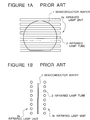
- FIGS 1A and 1B there are shown schematic views of a semiconductor wafer which is treated by a typical conventional lamp annealing process.
- each surface of a semiconductor wafer 1 is exposed to infrared rays which are radiated from infrared lamp units 3a and 3b.
- the infrared lamp units 3a and 3b are respectively composed by multiple infrared radiating tubes 2 which are disposed closely in parallel with each other, so that the semiconductor wafer 1 is homogeneously exposed to infrared rays.
- the infrared radiating tubes 2 of the infrared lamp unit 3a are disposed orthogonally to those of the lamp unit 3b.
- the temperature of the semiconductor wafer 1 can be more precisely controlled than using an electric furnace.
- the inventors found that a significant temperature distribution is generated on the semiconductor wafer 1 and it has adversely effect on the properties of the semiconductor wafer 1.
- the unevenness of temperature distribution of the semiconductor wafer 1 is generated by the heat radiation from its edge and the temperature of a center portion of the semiconductor wafer 1 becomes higher than that of its edge.
- the difference of the temperatures tends to increase during cooling and the maximum difference of the temperatures may be more than 10°C.
- Another object of the present invention is to provide an apparatus for performing such a lamp annealing process.
- a lamp annealing process for a semiconductor wafer characterized in that infrared radiating lamps are arranged annularly and coaxially with said semiconductor wafer and said infrared radiating lamps are controlled individually so that the outer lamps radiate more heat flux than the inner lamps to cancel the unevenness of the temperature distribution of said semiconductor wafer which would otherwise be caused by the heat escape from the edges of said semiconductor wafer.
- the infrared radiation lamps preferably consist of multiple annular infrared tubes each of which has a different radius, and which are disposed coaxially with the semiconductor wafer. Otherwise, the infrared radiation lamps consist of multiple dot-like small halogen lamps arranged to form annular arrays each of which has a different radius, and which are disposed coaxially with the semiconductor wafer.
- Figures 1A and 1B are schematic views showing a semiconductor wafer which is treated by a conventional lamp annealing process;
- Figure 1A is a schematic elevation and
- Figure 1B is a side section;
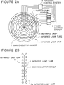
- Figures 2A and 2B are views similar to Figures 1A and 1B but showing a semiconductor wafer on which a lamp annealing process is performed by an apparatus in accordance with the present invention.
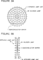
- Figures 3A and 3B are views similar to Figures 1A and 1B but showing a semiconductor wafer which is treated by another method performed by another apparatus in accordance with the present invention.
- FIGS 2A and 2B there are shown schematic views of a semiconductor wafer 1 which is annealed in a lamp annealing process in accordance with the present invention by using an apparatus in accordance with the present invention.
- a pair of infrared lamp units 3a and 3b are arranged in parallel with and separately to each other so that the wafer 1 to be annealed is put betweem the lamp units 3a and 3b but in parallel to and separately from each of the lamp units 3a and 3b.
- Each of the lamp units 3a and 3b consists of multiple annular special infrared lamp tubes 2 each of which has a different radius, and which are disposed coaxially on the same plane.
- a small dot-like infrared lamp 21 may be provided at the center of the annular infrared lamp tubes 2, if necessary.
- Each infrared lamp tube 2 is connected to an independent power control system 5, and the power control system 5 controls the heat output of the corresponding infrared lamp tube 2 individually.
- annular halogen lamp tubes and halogen lamp can be used instead of infrared lamp tubes 2 and infrared lamp 21, annular halogen lamp tubes and halogen lamp can be used.
- the semiconductor wafer 1 is placed between the infrared lamp units 3a and 3b coaxially with the infrared lamp tubes 2.
- the heat output of each infrared lamp tube 2 of the infrared lamp units 3a and 3b is controlled individually as described above, in such a manner that the outer it is located, the more heat flux it will be made to radiate.
- This heat output control makes the strength of heat radiation from each infrared lamp tube 2 to the semiconductor wafer be to correspond to the heat transfer which is caused by the heat escape from the edge of the semiconductor wafer 1 so as to make the temperature of the semiconductor wafer 1 homogeneous over the whole of the wafer 1.
- the infrared lamp units 3a and 3b are so controlled that the heat radiation of the infrared lamp tubes 2 have positive graduation in the direction of a radius which cancels unevenness of the temperature distribution of the semiconductor wafer 1.
- the heat output of each infrared lamp tube 2 can be controlled precisely so that unevenness of the temperature distribution of the semiconductor wafer 1 will be cancelled.
- the temperature sensors 6 and a feedback control system 7 are not always necessary. They are necessary only when annealing a semiconductor wafer of which the heat condition to cancel the unevenness of the temperature distribution is unknown. In case of annealing many semiconductor wafers, the semiconductor wafers can be treated in one heat condition. Therefore, once a good heat condition is found, it is possible to anneal other semiconductor wafers without the temperature sensors 6 and the feedback control system 7 by controlling the infrared lamp units in the same way by which the wafers can be treated in the good condition
- Figures 3A and 3B show another embodiment of the present invention in which the infrared lamp units 3a and 3b consist of multiple small dot-like halogen lamps 20.
- the halogen lamps 20 are disposed to form a plurality of coaxially annular arrays having difficult radii, and the halogen lamps 20 included in each annular array are connected in common to a independent power control system 5, as is the infrared lamp tubes 2 of Figure 2A.
Applications Claiming Priority (1)
| Application Number | Priority Date | Filing Date | Title |
|---|---|---|---|
| JP2196685A JPH0482215A (ja) | 1990-07-25 | 1990-07-25 | ランプアニール装置 |
Publications (2)
| Publication Number | Publication Date |
|---|---|
| EP0468874A2 true EP0468874A2 (de) | 1992-01-29 |
| EP0468874A3 EP0468874A3 (en) | 1992-06-03 |
Family
ID=16361894
Family Applications (1)
| Application Number | Title | Priority Date | Filing Date |
|---|---|---|---|
| EP19910402034 Withdrawn EP0468874A3 (en) | 1990-07-25 | 1991-07-22 | Lamp annealing process for semiconductor wafer and apparatus for execution of such process |
Country Status (2)
| Country | Link |
|---|---|
| EP (1) | EP0468874A3 (de) |
| JP (1) | JPH0482215A (de) |
Cited By (14)
| Publication number | Priority date | Publication date | Assignee | Title |
|---|---|---|---|---|
| EP0576791A1 (de) * | 1992-04-16 | 1994-01-05 | Texas Instruments Incorporated | Mehrzonale Beleuchtungseinrichtung mit versenkten Fühlern für Kontrolle des Verfahrens |
| EP0723289A2 (de) * | 1994-06-07 | 1996-07-24 | Texas Instruments Incorporated | Härtungsverfahren einer Verbundform für die Verkapselung von Halbleiterbauelementen |
| US5592581A (en) * | 1993-07-19 | 1997-01-07 | Tokyo Electron Kabushiki Kaisha | Heat treatment apparatus |
| US5689614A (en) * | 1990-01-19 | 1997-11-18 | Applied Materials, Inc. | Rapid thermal heating apparatus and control therefor |
| WO2000034986A1 (en) * | 1998-12-10 | 2000-06-15 | Steag Rtp Systems, Inc. | Rapid thermal processing chamber for processing multiple wafers |
| US6127288A (en) * | 1996-03-25 | 2000-10-03 | Sumitomo Electric Industries, Ltd. | Method of thermally processing semiconductor wafer |
| WO2000072636A1 (de) * | 1999-05-21 | 2000-11-30 | Steag Rtp Systems Gmbh | Vorrichtung und verfahren zum thermischen behandeln von substraten |
| WO2001063304A3 (en) * | 2000-02-23 | 2002-01-03 | Leo Martin Gibbs | Method and apparatus for isolated thermal fault finding in electronic components |
| US6717158B1 (en) | 1999-01-06 | 2004-04-06 | Mattson Technology, Inc. | Heating device for heating semiconductor wafers in thermal processing chambers |
| EP1429377A3 (de) * | 2002-12-13 | 2005-03-23 | Sanyo Electric Co., Ltd. | Verfahren zum Fliess-Glätten leitender Anschlüsse |
| US7169639B2 (en) | 2003-04-17 | 2007-01-30 | Sanyo Electric Co., Ltd. | Semiconductor device manufacturing method |
| US7919875B2 (en) | 2003-08-06 | 2011-04-05 | Sanyo Electric Co., Ltd. | Semiconductor device with recess portion over pad electrode |
| US8105856B2 (en) | 2002-04-23 | 2012-01-31 | Semiconductor Components Industries, Llc | Method of manufacturing semiconductor device with wiring on side surface thereof |
| CN114318547A (zh) * | 2021-12-24 | 2022-04-12 | 武汉嘉仪通科技有限公司 | 红外快速退火炉 |
Families Citing this family (4)
| Publication number | Priority date | Publication date | Assignee | Title |
|---|---|---|---|---|
| JPH113868A (ja) * | 1997-06-12 | 1999-01-06 | Nec Yamagata Ltd | ランプアニール装置およびランプアニール方法 |
| TWI229435B (en) | 2002-06-18 | 2005-03-11 | Sanyo Electric Co | Manufacture of semiconductor device |
| TWI227550B (en) | 2002-10-30 | 2005-02-01 | Sanyo Electric Co | Semiconductor device manufacturing method |
| TWI324800B (en) | 2005-12-28 | 2010-05-11 | Sanyo Electric Co | Method for manufacturing semiconductor device |
Family Cites Families (2)
| Publication number | Priority date | Publication date | Assignee | Title |
|---|---|---|---|---|
| JPS63143815A (ja) * | 1986-12-08 | 1988-06-16 | Matsushita Electric Ind Co Ltd | ランプアニ−ル装置 |
| JPS647519A (en) * | 1987-06-30 | 1989-01-11 | Oki Electric Ind Co Ltd | Annealing device |
-
1990
- 1990-07-25 JP JP2196685A patent/JPH0482215A/ja active Pending
-
1991
- 1991-07-22 EP EP19910402034 patent/EP0468874A3/en not_active Withdrawn
Cited By (24)
| Publication number | Priority date | Publication date | Assignee | Title |
|---|---|---|---|---|
| US5689614A (en) * | 1990-01-19 | 1997-11-18 | Applied Materials, Inc. | Rapid thermal heating apparatus and control therefor |
| EP0576791A1 (de) * | 1992-04-16 | 1994-01-05 | Texas Instruments Incorporated | Mehrzonale Beleuchtungseinrichtung mit versenkten Fühlern für Kontrolle des Verfahrens |
| US5592581A (en) * | 1993-07-19 | 1997-01-07 | Tokyo Electron Kabushiki Kaisha | Heat treatment apparatus |
| EP0723289A2 (de) * | 1994-06-07 | 1996-07-24 | Texas Instruments Incorporated | Härtungsverfahren einer Verbundform für die Verkapselung von Halbleiterbauelementen |
| US6235543B1 (en) | 1996-03-25 | 2001-05-22 | Sumitomo Electric Industries, Ltd. | Method of evaluating a semiconductor wafer |
| US6127288A (en) * | 1996-03-25 | 2000-10-03 | Sumitomo Electric Industries, Ltd. | Method of thermally processing semiconductor wafer |
| US6310328B1 (en) | 1998-12-10 | 2001-10-30 | Mattson Technologies, Inc. | Rapid thermal processing chamber for processing multiple wafers |
| WO2000034986A1 (en) * | 1998-12-10 | 2000-06-15 | Steag Rtp Systems, Inc. | Rapid thermal processing chamber for processing multiple wafers |
| US6610967B2 (en) | 1998-12-10 | 2003-08-26 | Mattson Technology, Inc. | Rapid thermal processing chamber for processing multiple wafers |
| US6727474B2 (en) | 1998-12-10 | 2004-04-27 | Mattson Technology, Inc. | Rapid thermal processing chamber for processing multiple wafers |
| US7038174B2 (en) | 1999-01-06 | 2006-05-02 | Mattson Technology, Inc. | Heating device for heating semiconductor wafers in thermal processing chambers |
| US8138451B2 (en) | 1999-01-06 | 2012-03-20 | Mattson Technology, Inc. | Heating device for heating semiconductor wafers in thermal processing chambers |
| US7608802B2 (en) | 1999-01-06 | 2009-10-27 | Mattson Technology, Inc. | Heating device for heating semiconductor wafers in thermal processing chambers |
| US6717158B1 (en) | 1999-01-06 | 2004-04-06 | Mattson Technology, Inc. | Heating device for heating semiconductor wafers in thermal processing chambers |
| US6771895B2 (en) | 1999-01-06 | 2004-08-03 | Mattson Technology, Inc. | Heating device for heating semiconductor wafers in thermal processing chambers |
| WO2000072636A1 (de) * | 1999-05-21 | 2000-11-30 | Steag Rtp Systems Gmbh | Vorrichtung und verfahren zum thermischen behandeln von substraten |
| US6614005B1 (en) | 1999-05-21 | 2003-09-02 | Steag Rtp Systems Gmbh | Device and method for thermally treating substrates |
| WO2001063304A3 (en) * | 2000-02-23 | 2002-01-03 | Leo Martin Gibbs | Method and apparatus for isolated thermal fault finding in electronic components |
| US8105856B2 (en) | 2002-04-23 | 2012-01-31 | Semiconductor Components Industries, Llc | Method of manufacturing semiconductor device with wiring on side surface thereof |
| EP1429377A3 (de) * | 2002-12-13 | 2005-03-23 | Sanyo Electric Co., Ltd. | Verfahren zum Fliess-Glätten leitender Anschlüsse |
| US7208340B2 (en) | 2002-12-13 | 2007-04-24 | Sanyo Electric Co., Ltd. | Semiconductor device manufacturing method |
| US7169639B2 (en) | 2003-04-17 | 2007-01-30 | Sanyo Electric Co., Ltd. | Semiconductor device manufacturing method |
| US7919875B2 (en) | 2003-08-06 | 2011-04-05 | Sanyo Electric Co., Ltd. | Semiconductor device with recess portion over pad electrode |
| CN114318547A (zh) * | 2021-12-24 | 2022-04-12 | 武汉嘉仪通科技有限公司 | 红外快速退火炉 |
Also Published As
| Publication number | Publication date |
|---|---|
| JPH0482215A (ja) | 1992-03-16 |
| EP0468874A3 (en) | 1992-06-03 |
Similar Documents
| Publication | Publication Date | Title |
|---|---|---|
| EP0468874A2 (de) | Lampen-Temperungsverfahren für Halbleiterscheiben und Vorrichtung zur Durchführung eines derartigen Verfahrens | |
| EP0119654B1 (de) | Ofen zur Wärmebehandlung von Halbleiterkörpern | |
| US4571486A (en) | Heating method of semiconductor wafer | |
| JP2961123B2 (ja) | 電磁放射照射による半導体円板の急速熱処理方法 | |
| US4493977A (en) | Method for heating semiconductor wafers by a light-radiant heating furnace | |
| US6345150B1 (en) | Single wafer annealing oven | |
| JP2004511907A (ja) | 赤外線で急速かつ均一に基板を加熱する装置 | |
| US4469529A (en) | Method for heating semiconductor wafer by means of application of radiated light with supplemental circumferential heating | |
| US4468259A (en) | Uniform wafer heating by controlling light source and circumferential heating of wafer | |
| US4535227A (en) | Method for heating semiconductor wafer by means of application of radiated light | |
| US4543472A (en) | Plane light source unit and radiant heating furnace including same | |
| US5253324A (en) | Conical rapid thermal processing apparatus | |
| US4525380A (en) | Heating method of semiconductor wafer | |
| JPS61198735A (ja) | フラツシユランプアニ−ル装置 | |
| JPH06177141A (ja) | 熱処理装置 | |
| JP3140227B2 (ja) | ウエハ熱処理方法およびこれに用いるガードリング構造 | |
| US4486652A (en) | Blackbody radiation source with constant planar energy flux | |
| JPS5917253A (ja) | 半導体ウエハの熱処理方法 | |
| JPS61129834A (ja) | 光照射型熱処理装置 | |
| GB2163898A (en) | Temperature control for use in ion implantation apparatus | |
| JPS59178718A (ja) | 半導体基体の処理装置 | |
| JP2007227461A (ja) | 熱処理装置および熱処理方法 | |
| JPS63112495A (ja) | 気相成長装置 | |
| US6023555A (en) | Radiant heating apparatus and method | |
| JP2003100651A (ja) | 基板熱処理装置 |
Legal Events
| Date | Code | Title | Description |
|---|---|---|---|
| PUAI | Public reference made under article 153(3) epc to a published international application that has entered the european phase |
Free format text: ORIGINAL CODE: 0009012 |
|
| AK | Designated contracting states |
Kind code of ref document: A2 Designated state(s): DE DK FR GB NL |
|
| PUAL | Search report despatched |
Free format text: ORIGINAL CODE: 0009013 |
|
| AK | Designated contracting states |
Kind code of ref document: A3 Designated state(s): DE DK FR GB NL |
|
| STAA | Information on the status of an ep patent application or granted ep patent |
Free format text: STATUS: THE APPLICATION IS DEEMED TO BE WITHDRAWN |
|
| 18D | Application deemed to be withdrawn |
Effective date: 19921204 |