EP0469543A2 - Circuit de traitement d'interruptions multiples - Google Patents
Circuit de traitement d'interruptions multiples Download PDFInfo
- Publication number
- EP0469543A2 EP0469543A2 EP91112791A EP91112791A EP0469543A2 EP 0469543 A2 EP0469543 A2 EP 0469543A2 EP 91112791 A EP91112791 A EP 91112791A EP 91112791 A EP91112791 A EP 91112791A EP 0469543 A2 EP0469543 A2 EP 0469543A2
- Authority
- EP
- European Patent Office
- Prior art keywords
- interrupt
- signal
- gate
- flip
- flop
- Prior art date
- Legal status (The legal status is an assumption and is not a legal conclusion. Google has not performed a legal analysis and makes no representation as to the accuracy of the status listed.)
- Withdrawn
Links
Images


Classifications
-
- G—PHYSICS
- G06—COMPUTING OR CALCULATING; COUNTING
- G06F—ELECTRIC DIGITAL DATA PROCESSING
- G06F9/00—Arrangements for program control, e.g. control units
- G06F9/06—Arrangements for program control, e.g. control units using stored programs, i.e. using an internal store of processing equipment to receive or retain programs
- G06F9/22—Microcontrol or microprogram arrangements
-
- G—PHYSICS
- G06—COMPUTING OR CALCULATING; COUNTING
- G06F—ELECTRIC DIGITAL DATA PROCESSING
- G06F13/00—Interconnection of, or transfer of information or other signals between, memories, input/output devices or central processing units
- G06F13/14—Handling requests for interconnection or transfer
- G06F13/20—Handling requests for interconnection or transfer for access to input/output bus
- G06F13/24—Handling requests for interconnection or transfer for access to input/output bus using interrupt
- G06F13/26—Handling requests for interconnection or transfer for access to input/output bus using interrupt with priority control
Definitions
- the present invention relates in general to handling an interrupt during execution of a program in a microcomputer, and more particularly to a multiple interrupt handling circuit for handling a multiplicity of interrupts and being internal IC-ed in a central processing unit (CPU) or peripheral IC-ed for connection with the CPU.
- CPU central processing unit
- peripheral IC-ed for connection with the CPU.
- an interrupt means that during execution of a program in a microcomputer a central control unit is forced to perform a control of another program beginning with a specific address.
- a conventional interrupt handling circuit upon generation of the interrupt in the course of execution of a program in the microcomputer, interrupts the execution of the program and, at this point of time, returns significant data in the central control unit to a main storage unit and then forces the central control unit to perform the control of another program beginning with the specific address. Namely, the operation of the central control unit branches off to a preset interrupt handling routine for performing it and at completion of the handling returns to the original program to continue to perform the original task.
- the conventional interrupt handling circuit has a disadvantage, in that it is impossible to handle a multiplicity of interrupts since it only allows the handling of one interrupt at a time.
- the present invention has been made in view of the above problem, and it is an object of the present invention to provide a multiple interrupt handling circuit for handling a multiplicity of interrupts with a priority being set.
- the object can be accomplished by providing a multiple interrupt handling circuit, comprising: mask register means for latching desired information from a microprocessor to generate a mask signal; latch register means for latching desired information from said microprocessor to generate a latch signal; a plurality of interrupt means, each for inputting said mask signal and said latch signal from said mask and latch register means and a corresponding interrupt input signal and generating in sequence a corresponding interrupt output signal in response to a clocking signal based on a system interrupt signal; encoding means for encoding said interrupt output signals from said plurality of interrupt means to generate a plurality of status signals; and control means for combining desired information signals from said microprocessor in read and write of information.
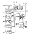
- FIG. 1 With reference to Fig. 1, there is shown a functional block diagram of a microcomputer system enabling a multiple interrupt handling in accordance with the present invention.
- the illustrated microcomputer comprises a microprocessor 1, an interrupt handling unit 2 for transferring an interrupt signal INT to the microprocessor 1, and an address decoder 3 for applying a control signal CS to the interrupt handling unit 2.
- the interrupt handling unit 2 of the present invention comprises a mask register 4 for latching desired information from the microprocessor 1 in response to a write signal WR1 to generate a mask signal MSK, a latch register 5 for latching desired information from the microprocessor 1 in response to a write signal WR2 to generate a latch signal L/T, a plurality of interrupt units 6 each for inputting a corresponding interrupt input signal INT1-INTn (wherein n is a positive integer), the mask signal MSK and the latch signal L/T from the mask and latch registers 4 and 5 respectively at an interrupt input terminal, a mask input terminal and a latch input terminal and generating in sequence a corresponding interrupt output signal INT01-INTOn in response to a clocking signal CLK based on the interrupt signal INT, an encoder 7 for encoding the interrupt output signals INT01-INTOn from the interrupt units 6 to generate a plurality
- interrupt handling unit 2 of the preferred embodiment is constructed such that sixteen interrupts can be handled, the number of interrupts to be handled may be modified.
- FIG. 3 there is shown a detailed circuit diagram of one of the interrupt units 6.
- constructions of the interrupt units 6 are identical to each other and hence only construction of the interrupt unit 6 will be illustrated and described which inputs the interrupt input signal INT1 and outputs the interrupt output signal INT01.
- the interrupt unit 6 is provided with an OR gate OR1 for inputting the interrupt input signal INT1 and the mask signal MSK and ORing the signals INT1 and MSK, a NOR gate NOR for NORing art output signal from the OR gate OR1 and the latch signal L/T, a D flip-flop FF1 including an input terminal for inputting power source Vcc and a clock terminal for inputting the output terminal from the OR gate OR1 as a clock pulse signal, an OR gate OR2 for ORing an output signal from the NOR gate NOR and an output signal from the D flip-flop FF1, an AND gate AND2 for ANDing an inverted one of an output signal from the OR gate OR2 and the clocking signal CLK, and a D flip-flop FF2 including an input terminal for inputting the output signal from the OR gate OR2 and a clock terminal for inputting the clocking signal CLK as a clock pulse signal.
- OR gate OR1 for inputting the interrupt input signal INT1 and the mask signal MSK and ORing the signals INT1 and MSK
- Table 1 represents how the encoder 7 handles sixteen interrupts.
- the number of interrupts may be modified as mentioned above and hence the processing capacity of the decoder 3 may be enlarged or reduced in accordance with the number of interrupts to be used, so as to handle the desired number of interrupts.
- the mask and latch registers 4 and 5 latch the desired information from the microprocessor 1 and outputs the mask and latch signals MSK and L/T to one input terminals of the OR gate OR1 and NOR gate NOR, respectively.
- the mask signal MSK is logic "1”
- the corresponding interrupt input signal, or the interrupt input signal INT1 as shown in Fig. 3 applied to the other input terminal of the OR gate OR1 is masked; when the mask signal MSK is logic "0", the OR gate OR1 operates to make the interrupt input signal INT1 available.
- the output signal from the NOR gate NOR is always logic “0" independent of the logic of the output signal from the OR gate OR1.
- the output signal from the OR gate OR1 through the D flip-flop FF1 is inputted to the D flip-flop FF2 via the OR gate OR2 for use in detection of a transition of the interrupt input signal INT1.
- the interrupt input signal INT1 through the OR gate OR1 is inputted directly to the D flip-flop FF2 via the NOR and OR gates NOR and OR2, thereby resulting in generation of an interrupt signal in accordance with a level of the interrupt input signal INT1.
- the interrupt input signal INT1 is applied to the interrupt input terminal of the interrupt unit 6 such that at the trailing edge the output signal from the OR gate OR1 sets the D flip-flop FF1 and then is inputted to the D flip-flop FF2 via the OR gate OR2.
- the external clocking signal CLK is applied via an AND gate AND1 in Fig. 2 to the AND gate AND2 in the interrupt unit 6 which does not receive any interrupt yet.
- the logic "1" signal is applied to the input terminal D of the D flip-flop FF2 so that the interrupt output signal INTO is set to logic "1" and, at the same time, the logic "1" " signal is applied to a clear terminal CLR of the D flip-flop FF1 so that the D flip-flop FF1 is cleared.
- the interrupt output signal INTO is applied to the encoder 7 so that the interrupt signal INT becomes active-low and hence the corresponding status signals S1-S4 are produced.
- the microprocessor 1 Upon receiving the interrupt signal INT, the microprocessor 1 reads the status signals S1-S4 to determine an interrupt state and then generates an interrupt clear signal INTCLR based on an interrupt address signal INTA to clear the D flip-flop FF2, so as to return the D flip-flop FF2 to its initial state.
- interrupt signal INT when a plurality of interrupt signals are generated simultaneously, one near to the interrupt input signal INT1 is set to have a high priority. As a result, if the interrupt signal INT is active by a higher priority one of the interrupt input signals INT1-INT2, the remaining interrupt input signals are stayed at a waiting state. Therefore, the circuit operates on the next order interrupt input signal after the status signals S1-S4 have been read and then the interrupt signal INT has been cleared.
- the interrupt signal INT is active-low by generation of interrupt, the output signal from the cleared D flip-flop FF1 in the interrupt unit 6 becomes logic "0", but the clocking signal continues to be maintained at logic "0" by the AND gate AND1 so that the logic "0" output signal from the D flip-flop FF1 are not latched into the D flip-flop FF2, thereby allowing the state of the D flip-flop FF2 to be maintained naturally.
- the active-low interrupt signal INT1 is turned into an active-high signal by passing through the OR gate OR1, the NOR gate NOR and the OR gate OR2 in order.
- the following operation is the same as that of the transition detection mode and hence that will not be described in detail.
- the D flip-flop FF1 has no effect on the whole system operation.
- the multiple interrupt handling circuit of the present invention can be IC-ed such that it can be used as an interrupt handling-dedicated IC and contained in the central processing unit, thereby allowing its simple construction.
Landscapes
- Engineering & Computer Science (AREA)
- Theoretical Computer Science (AREA)
- Software Systems (AREA)
- Physics & Mathematics (AREA)
- General Engineering & Computer Science (AREA)
- General Physics & Mathematics (AREA)
- Bus Control (AREA)
Applications Claiming Priority (2)
| Application Number | Priority Date | Filing Date | Title |
|---|---|---|---|
| KR1019900011655A KR920003152A (ko) | 1990-07-31 | 1990-07-31 | 다중 인터럽트 처리회로 |
| KR1165590 | 1990-07-31 |
Publications (2)
| Publication Number | Publication Date |
|---|---|
| EP0469543A2 true EP0469543A2 (fr) | 1992-02-05 |
| EP0469543A3 EP0469543A3 (en) | 1992-07-15 |
Family
ID=19301811
Family Applications (1)
| Application Number | Title | Priority Date | Filing Date |
|---|---|---|---|
| EP19910112791 Withdrawn EP0469543A3 (en) | 1990-07-31 | 1991-07-30 | Multiple interrupt handling circuit |
Country Status (2)
| Country | Link |
|---|---|
| EP (1) | EP0469543A3 (fr) |
| KR (1) | KR920003152A (fr) |
Cited By (8)
| Publication number | Priority date | Publication date | Assignee | Title |
|---|---|---|---|---|
| EP0657806A1 (fr) * | 1993-12-09 | 1995-06-14 | Pitney Bowes Inc. | Appareil de commande d'interruption pour circuit intégré |
| EP0742522A1 (fr) * | 1995-05-12 | 1996-11-13 | STMicroelectronics Limited | Commande d'interruption de processeur |
| GB2357902A (en) * | 1996-06-03 | 2001-07-04 | Nec Corp | A semiconductor device having fluorine doped silicon oxide films |
| US6272585B1 (en) | 1997-06-13 | 2001-08-07 | Alcatel | Multiple interrupt handling method and apparatus |
| US8738830B2 (en) | 2011-03-03 | 2014-05-27 | Hewlett-Packard Development Company, L.P. | Hardware interrupt processing circuit |
| US9189283B2 (en) | 2011-03-03 | 2015-11-17 | Hewlett-Packard Development Company, L.P. | Task launching on hardware resource for client |
| US9645823B2 (en) | 2011-03-03 | 2017-05-09 | Hewlett-Packard Development Company, L.P. | Hardware controller to choose selected hardware entity and to execute instructions in relation to selected hardware entity |
| WO2018144583A1 (fr) * | 2017-01-31 | 2018-08-09 | Texas Instruments Incorporated | Procédé et appareil de gestion d'interruption pour périphériques lents |
Family Cites Families (2)
| Publication number | Priority date | Publication date | Assignee | Title |
|---|---|---|---|---|
| US3611305A (en) * | 1969-02-10 | 1971-10-05 | Scanders Associates Inc | Data processor interrupt system |
| CA1319441C (fr) * | 1988-09-09 | 1993-06-22 | Paul R. Culley | Controleur d'interruption programmable |
-
1990
- 1990-07-31 KR KR1019900011655A patent/KR920003152A/ko not_active Withdrawn
-
1991
- 1991-07-30 EP EP19910112791 patent/EP0469543A3/en not_active Withdrawn
Cited By (12)
| Publication number | Priority date | Publication date | Assignee | Title |
|---|---|---|---|---|
| EP0657806A1 (fr) * | 1993-12-09 | 1995-06-14 | Pitney Bowes Inc. | Appareil de commande d'interruption pour circuit intégré |
| EP0742522A1 (fr) * | 1995-05-12 | 1996-11-13 | STMicroelectronics Limited | Commande d'interruption de processeur |
| US5867687A (en) * | 1995-05-12 | 1999-02-02 | Sgs-Thomson Microelectronics Limited | Microprocessor system for handling multiple priority levels interrupt requests to processor and interrupt process identifiers |
| GB2357902A (en) * | 1996-06-03 | 2001-07-04 | Nec Corp | A semiconductor device having fluorine doped silicon oxide films |
| GB2357902B (en) * | 1996-06-03 | 2001-08-15 | Nec Corp | Semiconductor device and method for manufacturing same |
| US6272585B1 (en) | 1997-06-13 | 2001-08-07 | Alcatel | Multiple interrupt handling method and apparatus |
| US8738830B2 (en) | 2011-03-03 | 2014-05-27 | Hewlett-Packard Development Company, L.P. | Hardware interrupt processing circuit |
| US9189283B2 (en) | 2011-03-03 | 2015-11-17 | Hewlett-Packard Development Company, L.P. | Task launching on hardware resource for client |
| US9645823B2 (en) | 2011-03-03 | 2017-05-09 | Hewlett-Packard Development Company, L.P. | Hardware controller to choose selected hardware entity and to execute instructions in relation to selected hardware entity |
| WO2018144583A1 (fr) * | 2017-01-31 | 2018-08-09 | Texas Instruments Incorporated | Procédé et appareil de gestion d'interruption pour périphériques lents |
| US10788853B2 (en) | 2017-01-31 | 2020-09-29 | Texas Instruments Incorporated | Interrupt handling method and apparatus for slow peripherals |
| US12105550B2 (en) | 2017-01-31 | 2024-10-01 | Texas Instruments Incorporated | Interrupt handling method and apparatus for slow peripherals |
Also Published As
| Publication number | Publication date |
|---|---|
| KR920003152A (ko) | 1992-02-29 |
| EP0469543A3 (en) | 1992-07-15 |
Similar Documents
| Publication | Publication Date | Title |
|---|---|---|
| US5079693A (en) | Bidirectional FIFO buffer having reread and rewrite means | |
| NL8900608A (nl) | Programmeerbare verwerkingsinrichting voor integratie op grote schaal. | |
| SU1541619A1 (ru) | Устройство дл формировани адреса | |
| CA1148665A (fr) | Microordinateur avec memoire a acces direct | |
| EP0469543A2 (fr) | Circuit de traitement d'interruptions multiples | |
| KR900002438B1 (ko) | 프로세서간 결합방식 | |
| EP0240606A2 (fr) | Système de traitement en pipeline et microprocesseur utilisant le système | |
| JPH0434177B2 (fr) | ||
| EP0012242B1 (fr) | Processeur de données digitales pour le traitement orienté vers le mot et le caractère | |
| US5604876A (en) | Apparatus for handling differing data length instructions using either directly specified or indirectly specified data lengths | |
| KR930005771B1 (ko) | 인터럽트 제어회로 | |
| US4723258A (en) | Counter circuit | |
| US6317825B1 (en) | Microprocessor comprising bit concatenation means | |
| JPH02126321A (ja) | 命令コードのデコード装置 | |
| JP3338722B2 (ja) | カウンタ回路 | |
| JP2922963B2 (ja) | シーケンスコントローラ | |
| JPS6349816B2 (fr) | ||
| SU1425692A2 (ru) | Двухканальное устройство дл сопр жени двух электронно-вычислительных машин | |
| KR100186505B1 (ko) | 인터럽트 발생회로 | |
| JPH05120079A (ja) | 動作履歴記憶装置 | |
| JPS629926B2 (fr) | ||
| JPH03134738A (ja) | マイクロプロセッサ | |
| JPS6354630A (ja) | デ−タ処理装置 | |
| JPH0695304B2 (ja) | デ−タ処理装置 | |
| JPS5998249A (ja) | デイジタル情報処理装置 |
Legal Events
| Date | Code | Title | Description |
|---|---|---|---|
| PUAI | Public reference made under article 153(3) epc to a published international application that has entered the european phase |
Free format text: ORIGINAL CODE: 0009012 |
|
| 17P | Request for examination filed |
Effective date: 19910828 |
|
| AK | Designated contracting states |
Kind code of ref document: A2 Designated state(s): DE FR IT |
|
| PUAL | Search report despatched |
Free format text: ORIGINAL CODE: 0009013 |
|
| AK | Designated contracting states |
Kind code of ref document: A3 Designated state(s): DE FR IT |
|
| STAA | Information on the status of an ep patent application or granted ep patent |
Free format text: STATUS: THE APPLICATION IS DEEMED TO BE WITHDRAWN |
|
| 18D | Application deemed to be withdrawn |
Effective date: 19930116 |