EP0470574A2 - Mehrprozessorsystem mit Cache-Speichern und Verfahren zur Steuerung von Cache-Speichern, um die Kohärenz zwischen ihnen aufrechtzuerhalten - Google Patents
Mehrprozessorsystem mit Cache-Speichern und Verfahren zur Steuerung von Cache-Speichern, um die Kohärenz zwischen ihnen aufrechtzuerhalten Download PDFInfo
- Publication number
- EP0470574A2 EP0470574A2 EP91113197A EP91113197A EP0470574A2 EP 0470574 A2 EP0470574 A2 EP 0470574A2 EP 91113197 A EP91113197 A EP 91113197A EP 91113197 A EP91113197 A EP 91113197A EP 0470574 A2 EP0470574 A2 EP 0470574A2
- Authority
- EP
- European Patent Office
- Prior art keywords
- cache memory
- memory
- write
- address
- cache
- Prior art date
- Legal status (The legal status is an assumption and is not a legal conclusion. Google has not performed a legal analysis and makes no representation as to the accuracy of the status listed.)
- Withdrawn
Links
Images









Classifications
-
- G—PHYSICS
- G06—COMPUTING OR CALCULATING; COUNTING
- G06F—ELECTRIC DIGITAL DATA PROCESSING
- G06F12/00—Accessing, addressing or allocating within memory systems or architectures
- G06F12/02—Addressing or allocation; Relocation
- G06F12/08—Addressing or allocation; Relocation in hierarchically structured memory systems, e.g. virtual memory systems
- G06F12/0802—Addressing of a memory level in which the access to the desired data or data block requires associative addressing means, e.g. caches
- G06F12/0806—Multiuser, multiprocessor or multiprocessing cache systems
- G06F12/0815—Cache consistency protocols
- G06F12/0831—Cache consistency protocols using a bus scheme, e.g. with bus monitoring or watching means
- G06F12/0833—Cache consistency protocols using a bus scheme, e.g. with bus monitoring or watching means in combination with broadcast means (e.g. for invalidation or updating)
Definitions
- the present invention relates to a multiprocessor system in which a plurality of cache memories and at least one common memory are connected via a system bus. More particularly, it relates to a technique of controlling a buffer invalidation processing for invalidating corresponding regions in other cache memories when respective write requests are generated simultaneously for the corresponding regions in the respective cache memories, to thereby maintain a coherency of data between the cache memories.
- An object of the present invention is to provide a cache memory control system which makes it possible to reflect an updated data on another cache memory even if data is newly written into a corresponding entry in the self cache memory after the transfer of the entry to another cache memory, and thus contributes to an improvement in the performance of the entire system.
- Another object of the present invention is to provide a buffer invalidation control system which makes it possible to invalidate corresponding regions in other cache memories without losing data rewritten in a certain cache memory and utilize the merit of a copy-back cache memory (high speed operation) to the maximum extent, to thereby contribute to an improvement in the performance of the entire system.
- a multiprocessor system in which a plurality of cache memories and at least one common memory are connected via a system bus, at least one of the plurality of cache memories being a copy-back cache memory, the copy-back cache memory including: a memory unit including a data region, an address region, a validation indication flag for indicating whether a region indicated by an access address exists in the self cache memory, a modified status indication flag for indicating whether data is rewritten, and a shared status indication flag for indicating whether an identical data is shared with other cache memories; a first unit, operatively connected to the memory unit, for intercepting a response of the common memory to an access when it detects the access from another cache memory to a region which is owned by the self cache memory and has already been rewritten and has not yet been reflected on the common memory; a second unit, operatively connected to the memory unit and the first unit, for transferring to the other cache memory an entry corresponding to a region indicated by the access address from the other cache memory
- a multiprocessor system in which a plurality of copy-back cache memories and at least one common memory are connected via a system bus, each cache memory including: a memory unit including a data region, an address region, a validation indication flag for indicating whether a region indicated by an access address exists in the self cache memory, and a modified status indication flag for indicating whether data is rewritten; a register unit for storing an address and data based on a write request from a corresponding CPU; a unit, operatively connected to the memory unit and the register unit, for storing a write data by the write request from the corresponding CPU in an object entry and the register unit to turn ON the modified status indication flag and sending out to the system bus a buffer invalidation request command including a part of the write address when the object region is registered in the self cache memory and the modified status indication flag is OFF in the case of an occurrence of the write request from the corresponding CPU; a unit, operatively connected to the memory unit, for monitoring a command
- a multiprocessor system in which a plurality of copy-back cache memories and at least one common memory are connected via a system bus, each cache memory including: a memory unit including a data region, an address region, a validation indication flag for indicating whether a region indicated by an access address exists in the self cache memory, and a modified status indication flag for indicating whether data is rewritten; a unit, operatively connected to the memory unit, for sending out to the system bus a buffer invalidation request command including a part of a write address from a corresponding CPU when the object region is registered in the self cache memory and the modified status indication flag is OFF in the case of an occurrence of the write request from the corresponding CPU; a unit, operatively connected to the memory unit and the sending unit, for monitoring a command on the system bus and, where the command is a buffer invalidation request command from another cache memory, canceling an address region included in the command out of the self cache memory; a register unit for retaining an address of the
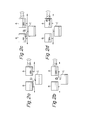
- FIGS 1 a to 1 e illustrate a manner of a conventional cache memory control, in the form of time sequence.
- a cache memory "A” is a copy-back one and a cache memory "B” is a write-through one.
- FIGS. 2a to 2d illustrate another manner of a conventional cache memory control, in the form of time sequence. Note, the references used are similar to those used in Fig. 1 a to 1 e.
- Figs.3 (a) and (b) show the status transition situation of cache memory "A" respectively in Fig. 1 and Fig. 2.
- Figures 3a and 3b show manners of a status transition of the cache memory "A" shown in Figs. 1 a to 1 and Figs. 2a to 2d, respectively.
- the intercept and the cache-to-cache transfer are carried out.
- FIGS 4a and 4b show the principle of the cache memory control according to the present invention.
- the present cache memory control is applied to a multiprocessor system in which a plurality of cache memories M1 to Mn and at least one common memory CM are connected via a system bus. At least one (M i ) of the plurality of cache memories is a copy-back one.
- the copy-back cache memory M 1 includes: a memory unit including a data region D, an address region A, a validation indication flag V for indicating whether a region indicated by an access address exists in the self cache memory, a modified status indication flag M for indicating whether data is rewritten, and a shared status indication flag S for indicating whether an identical data is shared with other cache memories; a first unit P1, operatively connected to the memory unit, for intercepting a response of the common memory to an access when it detects the access from another cache memory to a region which is owned by the self cache memory and has already been rewritten and has not yet been reflected on the common memory; a second unit P2, operatively connected to the memory unit and the first unit, for transferring to the other cache memory an entry corresponding to a region indicated by the access address from the other cache memory and turning ON the shared status indication flag; and a third unit P3, operatively connected to the memory unit and the second unit, for sending out a write address to the system bus and turning OFF the shared status indication flag where
- the copy-back cash memory M 1 intercepts the response of the common memory to the access and transfers the entry concerned to the other cache memory. As a result, both the cache memory M 1 and the other cache memory share an identical data and thus the shared status indication flag "S" is turned ON.
- the cache memory M 1 sends out the write address to the system bus.
- the other cache memory can detect that a new data has been written into the entry concerned which has been transferred immediately before it, and can clear (invalidate) the entry concerned.
- the cache memory M 1 since the updated data (the data after the write) in the entry concerned does not coincide with the data which has been transferred before the write, the cache memory M 1 turns OFF the shared status indication flag "S".
- the other cache memory can invalidate the entry concerned. Accordingly, it is possible to remove a disadvantage that an old data is adopted as the object of the operation. In this case, it is possible to reflect the updated data in the cache memory M 1 on the other cache memory by effecting an access when necessary. This contributes to an improvement in the performance of the entire system.
- Figure 5 illustrates a constitution of a closely coupled multiprocessor system to which the cache memory control according to this invention is applied.
- a plurality of cache memories which include copy-back cache memories 1A and write-through cache memories 1 B in mixture (in the present embodiment, only one copy-back cache memory and one write-through cache memory are shown for simplification of the illustration) are connected via a system bus 4 to at least one common memory 3 (only one is shown for simplification of the illustration).
- central processing units (CPUs) 2A and 2B each for controlling the supply of address information to the corresponding cache memory and the read/write of data are connected to the respective cache memories 1 A and 1 B, respectively.
- Figure 6 illustrates an internal constitution of the copy-back cache memory 1A.
- reference 31 is a tag area (tag memory) which has an address area to memorize the physical address of access data, and three status flags, namely a valid indication flag (V) to indicate whether a region indicated by an access address exists in the self cache memory or not, a modified status indication flag (M) to indicate whether data is rewritten or not, and a shared status indication flag (S) to indicate whether an identical data is shared with the other cache memories or not.
- V valid indication flag
- M modified status indication flag
- S shared status indication flag
- Reference 32 denotes a decoder (DEC) for decoding an address ADD1 from the corresponding CPU; reference 33 a comparator for detecting a coincidence or incoincidence between the address which has been registered in the tag area 31 and the address ADD1 from the CPU; reference 34 an AND gate for responding to the output and valid indication flag "V" of the comparator; reference 35 a decoder (DEC) for decoding an address ADD2 on the system bus 4; reference 36 a comparator for detecting a coincidence or incoincidence between the address which has been registered in the tag area 31 and the address ADD2 on the system bus 4; and reference 37 an AND gate for responding to the output and valid indication flag V of the comparator 36.
- DEC decoder
- Reference 38 denotes an external access supervisor, which responds to the output of AND gate 37 and the modified status indication flag "M” of AND gate 37, and has the functions of not simply sending out to the system bus 4 the intercept signal "INT” (the response intercept signal to the common memory 3) but also activating the transfer of data between cache memories to further turn ON the shared status indication flag "S".
- reference 39 denotes a CPU access controller, which has the functions of not only responding to the output of AND gate 34 and read/write control signals R/W from CPU as well as the modified status indication flag "M” and the shared status indication flag "S” to perform the usual processings, namely the hit/miss processing of cache and the bit renewal processing of flags "V” and “M” but also sending out the write address "WADD" to the system bus 4 and moreover turning OFF the shared status indication flag "S".
- the cache memory 1A sends out the write address to the system bus 4 because the shared status indication flag "S" is ON.
- the write address is sent out by the write-through manner or in the form of buffer invalidation request command.
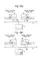
- Figs. 8a to 8e An example thereof is shown in Figs. 8a to 8e.
- reference 1 B' denotes a copy-back cache memory.
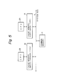
- Figure 9 shows the manner of a status transition of the copy-back cache memory 1A shown in Fig. 5.
- the intercept and the cache-to-cache transfer are carried out during the transition to the status "SM” from the status "M”
- the write address is sent out during the transition to the status "M” from the status "SM”.
- the cache memory 1 B can invalidate the entry concerned. Accordingly, it is possible to remove a disadvantage that an old data is adopted as the object of the operation. In this case, it is possible to reflect the updated data in the cache memory 1A on the cache memory 1B by effecting an access when necessary.
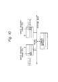
- Figure 10 shows an example of a conventional cache memory control.
- V denotes a validation indication flag which indicates whether a region designated by an access address exists in the self cache memory or not
- M denotes a modified status indication flag which indicates whether data is rewritten or not.
- the cache memory "A” (or “B") sends out a buffer invalidation request command "BICMD" to the system bus (write-once operation) and thereby clears (invalidates) a corresponding region in the cash memory "B" (or “A”).
- the cache memory concerned sends out an intercept signal to the cache memory which has effected the external access, to thereby request a temporary interruption of the external access, and swaps out (copies back) data of one entry.
- the cache memory concerned executes the write-once (send-out of the buffer invalidation request command) again after the access by the device (other cash memory) which has output the intercept signal is completed.
- Fig. 11 shows the manner of a status transition of the cache memory shown in Fig. 10.
- the transition (4) to the status "I” from the status "U” and the transition (3) to the status "I” from the status "M” are executed by the clear operation based on the buffer invalidation request command from the other cache memory.
- the write-once and the intercept operation are repeatedly carried out in the case that both the cache memories require the respective write-once, and a possibility occurs in that the write-once and the intercept operation fall down sometime into a limitless loop. For that reason, a problem occurs in that the high speed processing cannot be realized.
- Figures 12a and 12b show the principle of the buffer invalidation control according to one aspect of the present invention.
- Each cache memory Mi includes: a memory unit including a data region D, an address region A, a validation indication flag V for indicating whether a region indicated by an access address exists in the self cache memory, and a modified status indication flag M for indicating whether data is rewritten; a register unit PO for storing an address and data based on a write request from a corresponding CPU Ci; a unit P11, operatively connected to the memory unit and the register unit, for storing a write data by the write request from the corresponding CPU in an object entry and the register unit to turn ON the modified status indication flag and sending out to the system bus a buffer invalidation request command including a part of the write address when the object region is registered in the self cache memory and the modified status indication flag is OFF in the case of an occurrence of the
- the buffer invalidation request command from the cache memory M 1 is sent out on the system bus, and thus the cache memory M 2 cancels the buffer invalidation request command in the retention status (waiting status to send) and stores the data stored in the register unit P0, in the common memory CM (Prevention of the write data from disappearance).
- the cache memory M 1 can accept the write request from the corresponding CPU and return the response indicating the end of the write request. Also, since the buffer invalidation request command from the cache memory M 2 has been canceled, the data in the object region is prevented from being lost in the cache memory M i .
- each of the cache memories can renew the internal entry concerned and return the response of the write end to the corresponding CPU after the completion of the self write-once operation, and on the other hand, when the buffer invalidation request command is received, each cache memory can reflect the content of the register unit PO on the common memory CM in the write-through manner. Accordingly, it is possible to invalidate the corresponding region in the other cache memory without losing the rewritten data and thus utilize the high speed property which is the merit of a copy-back cache memory, to the maximum extent, to thereby contribute to the improvement in the efficiency of the entire system.
- Figure 13 illustrates a constitution of a closely coupled multiprocessor system to which the buffer invalidation control according to this invention is applied.
- a plurality of copy-back cache memories are connected via a system bus 4 to at least one common memory 3 (only one is shown for simplification of the illustration).
- central processing units (CPUs) 2A and 2B for controlling the supply of address information to the corresponding cache memories and the data read/write are connected to the respective cache memories 1 A and 1 B.
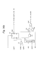
- Figures 14a and 14b illustrate an internal constitution of the cache memory 1A, 1B' shown in Fig. 13.
- reference 31 denotes a tag area (tag memory) which has an address area for memorizing the physical address of access data, a validation indication flag “V” for indicating whether a region indicated by an access address exists in the self cache memory or not, and a modified status indication flag “M” for indicating whether data is rewritten or not.
- the respective flags "V” and “M” represent “ON” or “1” when the respective conditions have been affirmed, and represent “OFF” or "0” when the conditions have been denied.
- Reference 32 denotes a decoder (DEC) for decoding an address ADD1 from the corresponding CPU; reference 33 a comparator responding to the address registered in the tag area 31, the address ADD1 from the CPU and the bit of the flag "V”; reference 34 an invertor responding to the read/write control signals "R/W” from the CPU; reference 35 an invertor responding to the bit of flag “M”; reference 36 an AND gate for making the bit of flag "M” to be set status (signal “MSET”) in response to the output of the comparator 33 and the output (CPU write signal "CWRT") of the invertor 34; reference 37 an AND gate responding to the output of the comparator 33, the output "CWRT” of the invertor 34 and the output of the invertor 35; reference 38 a store buffer for storing the address ADD1 from the corresponding CPU; and reference 39 a buffer invalidation controller having the functions of responding to the invalidation address "IAD" being supplied from the store buffer 38, the output WU and cancel signal CNL (to
- Reference 40 denotes a decoder (DEC) for decoding an address ADD2 on the system bus 4; reference 41 a comparator responding to the address registered in the tag area 31, the address "ADD2" on the system bus 4 and the bit of flag "V”; reference 42 a comparator responding to the invalidation address "IAD” (30 bits) being supplied from the store buffer 38 and the address "ADD2" (in this case, the address "BIAD” of buffer invalidation request command from the other cache memory) on the system bus 4; reference 43 a store buffer for storing the write data "WDT” from the corresponding CPU; and reference 44 a store operation controller having the functions of responding to the store address "SA” (32 bits) being supplied from the store buffer 38, the store data "SD” being supplied from the store buffer 43 and the store command starting signal “SCS” (to be described later) being output from the comparator 42, and of outputting the signal "SEND” for designa-ting the preparation of store command, the send-out to the system bus 4 and the end of the store operation
- the comparator 42 supplies the cancel signal "CNL” to the buffer invalidation controller 39 and supplies the store command starting signal "SCS" to the store operation controller 44.
- the circuit shown in Fig. 14b is constituted by an OR gate 51 which responds to the issuance/end indication signal "CIEND" of the buffer invalidation request command and the store operation end indication signal "SEND”; a J-K type flip-flop 52 for outputting the store buffer busy signal "SBB” to the Q-output terminal upon receipt of the CPU write signal "CWRT", the output of OR gate 51 and the external clock respectively to the J-terminal, K-terminal and clock-terminal "CLK”; a comparator 53 for detecting a coincidence or incoincidence between the invalidation address "IAD" from the store buffer 38 and the address "ADD1 from the CPU; an AND gate 54 for responding to the output of the comparator and the CPU write signal "CWRT”; an AND gate 55 for responding to the output of the AND gate and the store buffer busy signal "SBB”; and an AND gate 56 for responding to the output "WU” of the AND gate 37 (see Fig. 14a) and the store buffer busy signal "SBB” and an OR gate 56 for
- Figure 16 shows the manner of a status transition of the cache memory 1A, 1B' shown in Fig. 13.
- references “I”, “U”, “M”, (1), (3), (4) and (5) are the same as those used in Fig. 11 and thus the explanation is omitted.
- Reference “ST” denotes a waiting status for storing to the common memory
- reference “BI” denotes a waiting status for sending out the buffer invalidation request command.
- reference (2a) stands for a write into the unmodified region
- reference (2b) an issuance of the buffer invalidation request command
- reference (6) a waiting status for sending out the buffer invalidation request command
- reference (7) a detection of the buffer invalidation request command to the corresponding region
- reference (8) a waiting status for storing
- reference (9) a store completion.
- one cache memory 1A (1 B') can issue the buffer invalidation request command, rewrite the entry concerned after the end of the write-once operation and return the write end response to the CPU.
- the other cache memory 1B' (1 A) cancels the send-out wait status of the buffer invalidation request command in the self memory, receives the buffer invalidation request command from the one cache memory 1A (1B'), and writes the contents of the store buffers 38 and 43 into the common memory 3 in the write-through manner.
- Figures 17a to 17c show an example of a conventional cache memory control.
- the cache memory "A” when the data is written in an unmodified status region, the cache memory "A" sends out a buffer invalidation request command to the system bus ( 1).
- the cache memory "B” is also going to send out a buffer invalidation request command, it cannot occupy the system bus because the cache memory "A” has a quicker operation by chance. As a result, the cache memory “B” is brought to a "waiting status for sending out the buffer invalidation request command ( 2 ).
- the cache memory "B” is brought to a "store” wait status by the buffer invalidation request command from the cache memory "A".
- the "store” wait status stands for a status for storing the data in the corresponding region into the common memory "C”.
- the cache memory "A” since the cache memory "A” has finished sending out the buffer invalidation request command, it receives a write request from its corresponding CPU and returns a response indicating the write end to the CPU.
- the cache memory "B” stores the data which has been in the store wait status, in the common memory "C” ( 4 ).
- a disadvantage occurs in that, where the write requests are generated simultaneously to the respective corresponding regions of a plurality of copy-back cache memories (in the example of Figs. 17a to 17c, two cache memories "A" and "B"), the buffer invalidation request commands are sent out on the system bus from both the parties. Namely, as shown in the timing chart of Fig. 18, immediately after the buffer invalidation request command from the other cache memory is detected, the cancellation of the send-out of the buffer invalidation request command from the self cache memory is not in time. As a result, a problem arises in that the buffer invalidation request commands are sent out from both the cache memories and thus both the write data are lost or disappear.
- the system for writing the data in the object region simultaneously into the common memory "C" at the stage of 10 Item (1) can be proposed.
- This system fails to utilize the merit of a copy-back cache memory (decrease in the frequencies of bus access and the high speed processing caused thereby) to the maximum extent, and therefore a problem arises in that the performance of the entire system is lowered.
- Figure 19 shows the principle of the buffer invalidation control according to another aspect of the present invention.
- each cache memory Mi includes: a memory unit including a data region D, an address region A, a validation indication flag V for indicating whether a region indicated by an access address exists in the self cache memory, and a modified status indication flag M for indicating whether data is rewritten; a unit P21, operatively connected to the memory unit, for sending out to the system bus a buffer invalidation request command including a part of a write address from a corresponding CPU when the object region is registered in the self cache memory and the modified status indication flag is OFF in the case of an occurrence of the write request from the corresponding CPU; a unit P22, operatively connected to the memory unit and the sending unit, for monitoring a command on the system bus and, where the command is a buffer invalidation request command from another cache memory, canceling an address region included in the
- Each cache memory writes data into the unmodified region based on the write request from the corresponding CPU and then sends out the buffer invalidation request command to the system bus.
- the control is carried out such that the command concerned is ignored.
- the buffer invalidation request commands are issued in sequence to an identical region in a certain cache memory from a plurality of cache memories, the second and subsequent buffer invalidation request commands are ignored. Therefore, it is possible to realize the control of coincidence with the common memory without losing the data in the object region. Also, it is possible to utilize the merit of a copy-back cache memory to the maximum extent and thus contribute to an improvement of the performance of the entire system.
- Figure 20 illustrates another internal constitution of the cache memory (1A, 1B') shown in Fig. 13. Note, the portion enclosed by a broken line is the portion characterizing the present invention.
- reference 31 denotes a tag area (tag memory) which has an address area for memorizing the physical address of access data, a validation indication flag “V” for indicating whether a region indicated by an access address exists in the self cache memory or not, and a modified status indication flag “M” for indicating whether data is rewritten or not.
- the respective flags "V” and “M” represent “ON” or “1” when the respective conditions have been affirmed, and represent “OFF” or "0” when the conditions have been denied.
- Reference 32 denotes a decoder (DEC) for decoding an address "ADD1 from the corresponding CPU; reference 33 a comparator responding to the address registered into the tag area 31; the address "ADD1 from the CPU and the bit of flag "V”; reference 34 an invertor for responding to the read/write control signals “R/W” from the CPU; reference 35 an invertor for responding to the bit of flag “M”; reference 36 an AND gate for making the bit of flag "M” to be set status (signal “MSET”) in response to the output of the comparator 33 and the output of invertor 34 (CPU write signal "CWRT”); reference 37 an AND gate for responding to the output of the comparator 33, the output "CWRT” of invertor 34 and the output of invertor 35; reference 38 a store buffer for storing the address "ADD1 from the corresponding CPU; and reference 39 a buffer invalidation controlling circuit, which have the functions of responding to the address (invalidation address ) "IAD" of buffer invalidation request command being supplied from the store
- reference 40 denotes a decoder (DEC) for decoding the address "ADD2" on the system bus 4; reference 41 a comparator responding to the address registered into the tag area 31, the address "ADD2" on the system bus 4 and the bit of flag “V”; reference 42 a delay buffer for delaying by a given time the invalidation address "IAD” being supplied from the store buffer 38; reference 43 a comparator responding to the output address of the delay buffer and the address "ADD2" on the system bus 4 (the address "BIAD” of buffer invalidation request command from the other cache memory in this case); reference 44 an invertor responding to the output of the comparator 43; and reference 45 an AND gate for clearing (signal "VCLR”) the bit of flag "V” in response to the output of the invertor and the output of the comparator 41.
- DEC decoder
- Figure 22 shows the manner of another status transition of the cache memory 1A, 1B' shown in Fig. 13.
- the shift (6) to the status "I” from the status "U” and the shift (7) to the status "I” from the status "M” are executed by the clear operation based on
- each cache memory 1A (1B') functions, after sending out the buffer invalidation request command to the system bus, to ignore the command concerned once the buffer invalidation request command from the other cache memory 1B' (1 A) to the corresponding region has been detected within a predetermined period.
- the buffer invalidation request commands are issued in sequence to an identical region in a certain cache memory from a plurality of cache memories, the second and subsequent buffer invalidation request commands are controlled to be ignored.
Landscapes
- Engineering & Computer Science (AREA)
- Theoretical Computer Science (AREA)
- Physics & Mathematics (AREA)
- General Engineering & Computer Science (AREA)
- General Physics & Mathematics (AREA)
- Memory System Of A Hierarchy Structure (AREA)
Applications Claiming Priority (6)
| Application Number | Priority Date | Filing Date | Title |
|---|---|---|---|
| JP206851/90 | 1990-08-06 | ||
| JP2206851A JPH0492937A (ja) | 1990-08-06 | 1990-08-06 | キャッシュメモリ制御方式 |
| JP2210512A JPH0498352A (ja) | 1990-08-10 | 1990-08-10 | バッファ無効化制御方式 |
| JP210511/90 | 1990-08-10 | ||
| JP210512/90 | 1990-08-10 | ||
| JP2210511A JPH0498339A (ja) | 1990-08-10 | 1990-08-10 | バッファ無効化制御方式 |
Publications (2)
| Publication Number | Publication Date |
|---|---|
| EP0470574A2 true EP0470574A2 (de) | 1992-02-12 |
| EP0470574A3 EP0470574A3 (en) | 1992-07-08 |
Family
ID=27328692
Family Applications (1)
| Application Number | Title | Priority Date | Filing Date |
|---|---|---|---|
| EP19910113197 Withdrawn EP0470574A3 (en) | 1990-08-06 | 1991-08-05 | Multiprocessor system including cache memories and method of controlling cache memories to maintain coherence of data therebetween |
Country Status (2)
| Country | Link |
|---|---|
| EP (1) | EP0470574A3 (de) |
| KR (1) | KR940005769B1 (de) |
Cited By (6)
| Publication number | Priority date | Publication date | Assignee | Title |
|---|---|---|---|---|
| US5724549A (en) * | 1992-04-06 | 1998-03-03 | Cyrix Corporation | Cache coherency without bus master arbitration signals |
| EP0883131A3 (de) * | 1997-06-06 | 1999-12-01 | Matsushita Electric Industrial Co., Ltd. | Halbleiterspeicheranordnung wie z.B. Cachespeicher |
| US7296259B2 (en) * | 2002-09-11 | 2007-11-13 | Agere Systems Inc. | Processor system with cache-based software breakpoints |
| US7743215B2 (en) * | 2006-12-28 | 2010-06-22 | Fujitsu Limited | Cache-memory control apparatus, cache-memory control method and computer product |
| US20250378027A1 (en) * | 2024-06-07 | 2025-12-11 | Arm Limited | Invalidate-write hazard detection |
| US12619535B2 (en) * | 2024-06-07 | 2026-05-05 | Arm Limited | Invalidate-write hazard detection |
Family Cites Families (1)
| Publication number | Priority date | Publication date | Assignee | Title |
|---|---|---|---|---|
| EP0198574A3 (de) * | 1985-02-05 | 1989-11-29 | Digital Equipment Corporation | Vorrichtung und Verfahren zur Datenkopienübereinstimmung in einer Mehrcachespeicherdatenverarbeitungsanordnung |
-
1991
- 1991-08-05 EP EP19910113197 patent/EP0470574A3/en not_active Withdrawn
- 1991-08-06 KR KR1019910013593A patent/KR940005769B1/ko not_active Expired - Fee Related
Cited By (7)
| Publication number | Priority date | Publication date | Assignee | Title |
|---|---|---|---|---|
| US5724549A (en) * | 1992-04-06 | 1998-03-03 | Cyrix Corporation | Cache coherency without bus master arbitration signals |
| EP0883131A3 (de) * | 1997-06-06 | 1999-12-01 | Matsushita Electric Industrial Co., Ltd. | Halbleiterspeicheranordnung wie z.B. Cachespeicher |
| US6304943B1 (en) | 1997-06-06 | 2001-10-16 | Matsushita Electric Industrial Co., Ltd. | Semiconductor storage device with block writing function and reduce power consumption thereof |
| US7296259B2 (en) * | 2002-09-11 | 2007-11-13 | Agere Systems Inc. | Processor system with cache-based software breakpoints |
| US7743215B2 (en) * | 2006-12-28 | 2010-06-22 | Fujitsu Limited | Cache-memory control apparatus, cache-memory control method and computer product |
| US20250378027A1 (en) * | 2024-06-07 | 2025-12-11 | Arm Limited | Invalidate-write hazard detection |
| US12619535B2 (en) * | 2024-06-07 | 2026-05-05 | Arm Limited | Invalidate-write hazard detection |
Also Published As
| Publication number | Publication date |
|---|---|
| EP0470574A3 (en) | 1992-07-08 |
| KR940005769B1 (ko) | 1994-06-23 |
Similar Documents
| Publication | Publication Date | Title |
|---|---|---|
| EP0405882B1 (de) | Blockübertragungs- und Koprozessorschnittstellenbefehl | |
| EP0748481B1 (de) | Busarchitektur in hochgradiger pipeline-ausführung | |
| JP2541771B2 (ja) | 原子的メモリ参照方法及びシステム | |
| HK1002438B (en) | Move 16 block move and coprocessor interface instruction | |
| JPH09114665A (ja) | 記憶装置と補助プロセッサ間のコマンド及びデータ転送方法及び情報処理システム | |
| KR19990045059A (ko) | 캐시 메모리 시스템 | |
| JPH06309230A (ja) | バススヌ−プ方法 | |
| JPH06243108A (ja) | データ・コヒーレンシを維持する方法及びシステム | |
| WO1997004392A1 (en) | Shared cache memory device | |
| EP0470574A2 (de) | Mehrprozessorsystem mit Cache-Speichern und Verfahren zur Steuerung von Cache-Speichern, um die Kohärenz zwischen ihnen aufrechtzuerhalten | |
| US6862646B2 (en) | Method and apparatus for eliminating the software generated ready-signal to hardware devices that are not part of the memory coherency domain | |
| US7912998B2 (en) | DMA access systems and methods | |
| US6021472A (en) | Information processing device and control method thereof | |
| JPH06282528A (ja) | データ転送方法及びそのシステム | |
| JP3340047B2 (ja) | マルチプロセッサシステムおよび複製タグの制御方法 | |
| JPH0744459A (ja) | キャッシュ制御方法およびキャッシュ制御装置 | |
| JP3039391B2 (ja) | メモリシステム | |
| JP3757768B2 (ja) | ベクトルメモリアクセス時スカラメモリアクセス命令発行制御方式 | |
| JP3052460B2 (ja) | 協調処理型情報処理装置 | |
| JP3145479B2 (ja) | マルチプロセッサシステムとそのキャッシュメモリ制御方法および装置 | |
| JP3157740B2 (ja) | ベクトルデータ処理装置 | |
| JP2656558B2 (ja) | キャッシュメモリ制御回路 | |
| JPH0415496B2 (de) | ||
| JPH06309229A (ja) | データ処理装置 | |
| JP2791319B2 (ja) | データ処理装置 |
Legal Events
| Date | Code | Title | Description |
|---|---|---|---|
| PUAI | Public reference made under article 153(3) epc to a published international application that has entered the european phase |
Free format text: ORIGINAL CODE: 0009012 |
|
| AK | Designated contracting states |
Kind code of ref document: A2 Designated state(s): DE FR GB |
|
| PUAL | Search report despatched |
Free format text: ORIGINAL CODE: 0009013 |
|
| AK | Designated contracting states |
Kind code of ref document: A3 Designated state(s): DE FR GB |
|
| 17P | Request for examination filed |
Effective date: 19921226 |
|
| 17Q | First examination report despatched |
Effective date: 19971017 |
|
| STAA | Information on the status of an ep patent application or granted ep patent |
Free format text: STATUS: THE APPLICATION IS DEEMED TO BE WITHDRAWN |
|
| 18D | Application deemed to be withdrawn |
Effective date: 19990206 |