EP0471165A2 - Zuverlässiges supraleitendes Verbindungsglied für Dünnfilmbauelemente und Verfahren zur Herstellung - Google Patents
Zuverlässiges supraleitendes Verbindungsglied für Dünnfilmbauelemente und Verfahren zur Herstellung Download PDFInfo
- Publication number
- EP0471165A2 EP0471165A2 EP91109870A EP91109870A EP0471165A2 EP 0471165 A2 EP0471165 A2 EP 0471165A2 EP 91109870 A EP91109870 A EP 91109870A EP 91109870 A EP91109870 A EP 91109870A EP 0471165 A2 EP0471165 A2 EP 0471165A2
- Authority
- EP
- European Patent Office
- Prior art keywords
- bonding
- superconducting
- slab
- thin film
- link
- Prior art date
- Legal status (The legal status is an assumption and is not a legal conclusion. Google has not performed a legal analysis and makes no representation as to the accuracy of the status listed.)
- Granted
Links
Images

Classifications
-
- H—ELECTRICITY
- H01—ELECTRIC ELEMENTS
- H01R—ELECTRICALLY-CONDUCTIVE CONNECTIONS; STRUCTURAL ASSOCIATIONS OF A PLURALITY OF MUTUALLY-INSULATED ELECTRICAL CONNECTING ELEMENTS; COUPLING DEVICES; CURRENT COLLECTORS
- H01R4/00—Electrically-conductive connections between two or more conductive members in direct contact, i.e. touching one another; Means for effecting or maintaining such contact; Electrically-conductive connections having two or more spaced connecting locations for conductors and using contact members penetrating insulation
- H01R4/58—Electrically-conductive connections between two or more conductive members in direct contact, i.e. touching one another; Means for effecting or maintaining such contact; Electrically-conductive connections having two or more spaced connecting locations for conductors and using contact members penetrating insulation characterised by the form or material of the contacting members
- H01R4/68—Connections to or between superconductive connectors
-
- H—ELECTRICITY
- H01—ELECTRIC ELEMENTS
- H01R—ELECTRICALLY-CONDUCTIVE CONNECTIONS; STRUCTURAL ASSOCIATIONS OF A PLURALITY OF MUTUALLY-INSULATED ELECTRICAL CONNECTING ELEMENTS; COUPLING DEVICES; CURRENT COLLECTORS
- H01R43/00—Apparatus or processes specially adapted for manufacturing, assembling, maintaining, or repairing of line connectors or current collectors or for joining electric conductors
- H01R43/02—Apparatus or processes specially adapted for manufacturing, assembling, maintaining, or repairing of line connectors or current collectors or for joining electric conductors for soldered or welded connections
- H01R43/0207—Ultrasonic-, H.F.-, cold- or impact welding
-
- H—ELECTRICITY
- H10—SEMICONDUCTOR DEVICES; ELECTRIC SOLID-STATE DEVICES NOT OTHERWISE PROVIDED FOR
- H10W—GENERIC PACKAGES, INTERCONNECTIONS, CONNECTORS OR OTHER CONSTRUCTIONAL DETAILS OF DEVICES COVERED BY CLASS H10
- H10W72/00—Interconnections or connectors in packages
- H10W72/50—Bond wires
- H10W72/531—Shapes of wire connectors
- H10W72/5363—Shapes of wire connectors the connected ends being wedge-shaped
-
- Y—GENERAL TAGGING OF NEW TECHNOLOGICAL DEVELOPMENTS; GENERAL TAGGING OF CROSS-SECTIONAL TECHNOLOGIES SPANNING OVER SEVERAL SECTIONS OF THE IPC; TECHNICAL SUBJECTS COVERED BY FORMER USPC CROSS-REFERENCE ART COLLECTIONS [XRACs] AND DIGESTS
- Y10—TECHNICAL SUBJECTS COVERED BY FORMER USPC
- Y10S—TECHNICAL SUBJECTS COVERED BY FORMER USPC CROSS-REFERENCE ART COLLECTIONS [XRACs] AND DIGESTS
- Y10S505/00—Superconductor technology: apparatus, material, process
- Y10S505/70—High TC, above 30 k, superconducting device, article, or structured stock
- Y10S505/701—Coated or thin film device, i.e. active or passive
- Y10S505/703—Microelectronic device with superconducting conduction line
-
- Y—GENERAL TAGGING OF NEW TECHNOLOGICAL DEVELOPMENTS; GENERAL TAGGING OF CROSS-SECTIONAL TECHNOLOGIES SPANNING OVER SEVERAL SECTIONS OF THE IPC; TECHNICAL SUBJECTS COVERED BY FORMER USPC CROSS-REFERENCE ART COLLECTIONS [XRACs] AND DIGESTS
- Y10—TECHNICAL SUBJECTS COVERED BY FORMER USPC
- Y10S—TECHNICAL SUBJECTS COVERED BY FORMER USPC CROSS-REFERENCE ART COLLECTIONS [XRACs] AND DIGESTS
- Y10S505/00—Superconductor technology: apparatus, material, process
- Y10S505/70—High TC, above 30 k, superconducting device, article, or structured stock
- Y10S505/704—Wire, fiber, or cable
-
- Y—GENERAL TAGGING OF NEW TECHNOLOGICAL DEVELOPMENTS; GENERAL TAGGING OF CROSS-SECTIONAL TECHNOLOGIES SPANNING OVER SEVERAL SECTIONS OF THE IPC; TECHNICAL SUBJECTS COVERED BY FORMER USPC CROSS-REFERENCE ART COLLECTIONS [XRACs] AND DIGESTS
- Y10—TECHNICAL SUBJECTS COVERED BY FORMER USPC
- Y10S—TECHNICAL SUBJECTS COVERED BY FORMER USPC CROSS-REFERENCE ART COLLECTIONS [XRACs] AND DIGESTS
- Y10S505/00—Superconductor technology: apparatus, material, process
- Y10S505/80—Material per se process of making same
- Y10S505/812—Stock
- Y10S505/813—Wire, tape, or film
-
- Y—GENERAL TAGGING OF NEW TECHNOLOGICAL DEVELOPMENTS; GENERAL TAGGING OF CROSS-SECTIONAL TECHNOLOGIES SPANNING OVER SEVERAL SECTIONS OF THE IPC; TECHNICAL SUBJECTS COVERED BY FORMER USPC CROSS-REFERENCE ART COLLECTIONS [XRACs] AND DIGESTS
- Y10—TECHNICAL SUBJECTS COVERED BY FORMER USPC
- Y10S—TECHNICAL SUBJECTS COVERED BY FORMER USPC CROSS-REFERENCE ART COLLECTIONS [XRACs] AND DIGESTS
- Y10S505/00—Superconductor technology: apparatus, material, process
- Y10S505/825—Apparatus per se, device per se, or process of making or operating same
- Y10S505/917—Mechanically manufacturing superconductor
- Y10S505/927—Metallurgically bonding superconductive members
Definitions
- a reliable superconducting link, resistent to thermal cycling, is necessary in the construction of multicomponent superconducting devices, such as multichannel magnetometers, where simultaneous faultless operation of several superconducting devices is required. Such devices are used, for example, in the detection of feeble biomagnetic signals from the human brain.
- the prior art of superconducting bonding technology utilizes lead, tin-lead or niobium wires because these materials are sufficiently soft for mechanical bonding and their superconducting transition temperatures are well above the liquid helium temperature (e.g. S. Kiryu et al. in Advances in Biomagnetism, eds. S. J. Williamson, M. Hoke, G. Stroink, M. Kotani, Plenum Press, New York 1990).
- Lead, tin and their alloys melt at low temperatures (200-400 °C) so that the softening of these materials slightly below the melting point can be utilized in the bonding.
- niobium wire Ultrasound rather than heating is used when bonding with niobium wires because the melting point of Nb is very high (2470 °C). Compared to lead, niobium wire is also stiff so that to avoid too high stresses at the joints either long or very thin wires ( ⁇ 10 ⁇ m) must be used. Thin wires are difficult to handle and long wires come off easily during further handling of the bonded device. Long wires also require extra space and, especially in the magnetometer applications, form parasitic superconducting pickup loops. Tin and lead are too soft to be bonded with ultrasound. Wires made of these materials are usually pressed against the bonding pad of the thin film device by aid of a small, hot soldering tip.
- This invention describes a new type of superconducting lead or tin-lead link by which the problems associated with the prior art techniques described above can be avoided.
- the features characteristic to this superconducting joint are described in claims 1 and 2.
- the characteristics of the fabrication method are described in claims 4 and 5.
- the temperature of the relatively large planar interface between the flat wire and the bonding pad is essentially equal to the temperature of the bonding tip.
- the bonding temperature is easily controlled and can be maintained high enough, to ensure a good metal-to-metal contact at the joint, without melting the wire from the tip side.
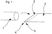
- Figure 1 the shaping of a contact wire blank into a thin, sliced contact slab is described.
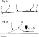
- Figure 2 shows the mounting of the slab, and
- Figure 3 illustrates the final double joint.
- the wire blank 1 of about 100 ⁇ m diameter, is pressed or rolled into a plate 2, which is about 10 ⁇ m thick and 3-4 mm wide.
- This plate is sliced with the desired number of partial cuts 4, and then detached from the blank with a long cut 5 into a final bonding slab 3.
- the slab is then placed to connect the devices located on two different substrates 6 and 7 so that its ends, as shown in figure 2a, rest on the contact pads 8 and 9.
- the slab is fixed from one of its ends by pressing with the hot soldering tip 10 against the bonding pad 8. After that the slab is bent as shown in figure 2b and bonded from the other end, too.
- Figure 3 is a cut view of the ready-made double joint showing the U-beam like deformation of the joint regime.
- the slab adapts to the relative motion of the bonding pads, caused by the differences in the thermal contraction, by bowing at the intentional bend 11 far from the U-beam like bonding regions.
Landscapes
- Physics & Mathematics (AREA)
- Condensed Matter Physics & Semiconductors (AREA)
- General Physics & Mathematics (AREA)
- Manufacturing Of Electrical Connectors (AREA)
- Superconductors And Manufacturing Methods Therefor (AREA)
- Multi-Conductor Connections (AREA)
- Coupling Device And Connection With Printed Circuit (AREA)
- Containers, Films, And Cooling For Superconductive Devices (AREA)
- Superconductor Devices And Manufacturing Methods Thereof (AREA)
- Inorganic Compounds Of Heavy Metals (AREA)
- Manufacture Of Macromolecular Shaped Articles (AREA)
- Treatments For Attaching Organic Compounds To Fibrous Goods (AREA)
- Surgical Instruments (AREA)
Applications Claiming Priority (2)
| Application Number | Priority Date | Filing Date | Title |
|---|---|---|---|
| FI904071A FI89643C (fi) | 1990-08-17 | 1990-08-17 | Supraledande fog foer tunnfilmkomponenter och metod foer dess tillverkning |
| FI904071 | 1990-08-17 |
Publications (3)
| Publication Number | Publication Date |
|---|---|
| EP0471165A2 true EP0471165A2 (de) | 1992-02-19 |
| EP0471165A3 EP0471165A3 (en) | 1992-03-04 |
| EP0471165B1 EP0471165B1 (de) | 1995-09-20 |
Family
ID=8530943
Family Applications (1)
| Application Number | Title | Priority Date | Filing Date |
|---|---|---|---|
| EP91109870A Expired - Lifetime EP0471165B1 (de) | 1990-08-17 | 1991-06-17 | Zuverlässiges supraleitendes Verbindungsglied für Dünnfilmbauelemente und Verfahren zur Herstellung |
Country Status (9)
| Country | Link |
|---|---|
| US (1) | US5148262A (de) |
| EP (1) | EP0471165B1 (de) |
| JP (1) | JP3121382B2 (de) |
| AT (1) | ATE128274T1 (de) |
| CA (1) | CA2045239C (de) |
| DE (1) | DE69113172T2 (de) |
| DK (1) | DK0471165T3 (de) |
| ES (1) | ES2077117T3 (de) |
| FI (1) | FI89643C (de) |
Cited By (1)
| Publication number | Priority date | Publication date | Assignee | Title |
|---|---|---|---|---|
| WO2000077864A1 (de) * | 1999-06-16 | 2000-12-21 | Siemens Aktiengesellschaft | Stromtragende verbindungselemente für plattenleiter aus hochtemperatur-supraleitenden dünnschichten |
Families Citing this family (4)
| Publication number | Priority date | Publication date | Assignee | Title |
|---|---|---|---|---|
| FR2678432B1 (fr) * | 1991-06-27 | 1993-09-03 | Alsthom Gec | Procede de liaison entre une ceramique supraconductrice a haute temperature critique et un conducteur supraconducteur a base de niobium-titane. |
| DE102006025867A1 (de) * | 2006-06-02 | 2007-12-06 | Robert Bosch Gmbh | Bondverbindung sowie Verfahren zum Bonden zweier Kontaktflächen |
| USD857420S1 (en) | 2016-12-23 | 2019-08-27 | Few Fahrzeugelektrikwerk Gmbh & Co. Kg | Mounting device |
| DE102016125781A1 (de) * | 2016-12-28 | 2018-06-28 | Few Fahrzeugelektrikwerk Gmbh & Co. Kg | Elektrisches Anschlusselement |
Family Cites Families (5)
| Publication number | Priority date | Publication date | Assignee | Title |
|---|---|---|---|---|
| FR2054506B1 (de) * | 1969-07-18 | 1975-08-22 | Thomson Csf | |
| US3855693A (en) * | 1973-04-18 | 1974-12-24 | Honeywell Inf Systems | Method for assembling microelectronic apparatus |
| JPS5449066A (en) * | 1977-09-27 | 1979-04-18 | Nec Corp | Semiconductor device |
| US4660061A (en) * | 1983-12-19 | 1987-04-21 | Sperry Corporation | Intermediate normal metal layers in superconducting circuitry |
| US4963523A (en) * | 1987-11-06 | 1990-10-16 | The United States Of America As Represented By The Secretary Of The Commerce | High-Tc superconducting unit having low contact surface resistivity and method of making. |
-
1990
- 1990-08-17 FI FI904071A patent/FI89643C/fi active IP Right Grant
-
1991
- 1991-06-17 EP EP91109870A patent/EP0471165B1/de not_active Expired - Lifetime
- 1991-06-17 ES ES91109870T patent/ES2077117T3/es not_active Expired - Lifetime
- 1991-06-17 DK DK91109870.5T patent/DK0471165T3/da active
- 1991-06-17 AT AT91109870T patent/ATE128274T1/de not_active IP Right Cessation
- 1991-06-17 DE DE69113172T patent/DE69113172T2/de not_active Expired - Fee Related
- 1991-06-21 CA CA002045239A patent/CA2045239C/en not_active Expired - Lifetime
- 1991-07-01 US US07/723,934 patent/US5148262A/en not_active Expired - Lifetime
- 1991-08-09 JP JP03200512A patent/JP3121382B2/ja not_active Expired - Lifetime
Cited By (1)
| Publication number | Priority date | Publication date | Assignee | Title |
|---|---|---|---|---|
| WO2000077864A1 (de) * | 1999-06-16 | 2000-12-21 | Siemens Aktiengesellschaft | Stromtragende verbindungselemente für plattenleiter aus hochtemperatur-supraleitenden dünnschichten |
Also Published As
| Publication number | Publication date |
|---|---|
| ES2077117T3 (es) | 1995-11-16 |
| DE69113172T2 (de) | 1996-02-15 |
| CA2045239A1 (en) | 1992-02-18 |
| FI89643C (fi) | 1993-10-25 |
| JP3121382B2 (ja) | 2000-12-25 |
| FI89643B (fi) | 1993-07-15 |
| CA2045239C (en) | 2002-04-09 |
| ATE128274T1 (de) | 1995-10-15 |
| DK0471165T3 (da) | 1995-11-06 |
| FI904071A0 (fi) | 1990-08-17 |
| US5148262A (en) | 1992-09-15 |
| EP0471165B1 (de) | 1995-09-20 |
| DE69113172D1 (de) | 1995-10-26 |
| FI904071A7 (fi) | 1992-02-18 |
| EP0471165A3 (en) | 1992-03-04 |
| JPH0696807A (ja) | 1994-04-08 |
Similar Documents
| Publication | Publication Date | Title |
|---|---|---|
| US4808769A (en) | Film carrier and bonding method using the film carrier | |
| JP3290055B2 (ja) | 素子を配置およびハンダ付けする方法 | |
| US4664309A (en) | Chip mounting device | |
| US4290079A (en) | Improved solder interconnection between a semiconductor device and a supporting substrate | |
| US5478006A (en) | Printed-circuit substrate and its connecting method | |
| US6214156B1 (en) | Semiconductor device mounted on board by flip-chip and method for mounting the same | |
| US5021630A (en) | Laser soldering method and apparatus | |
| US5970608A (en) | Cryogenic flex cable connector | |
| AU673626B2 (en) | Method of soldering an electric cable to a circuit board | |
| EP0471165B1 (de) | Zuverlässiges supraleitendes Verbindungsglied für Dünnfilmbauelemente und Verfahren zur Herstellung | |
| US5948175A (en) | Strap device clamping soldered wires for use in solar cell arrays | |
| EP0482940A1 (de) | Verfahren zur Herstellung einer elektrischen Verbindung für eine integrierte Schaltung | |
| US6347901B1 (en) | Solder interconnect techniques | |
| JPS6114798A (ja) | はんだ相互接続を形成する方法 | |
| KR930002280B1 (ko) | 반도체 회로소자 접촉 시스템 | |
| JP4919614B2 (ja) | 太陽電池装置、及び太陽電池装置の製造方法 | |
| US5225634A (en) | Hybrid circuit formed of two circuits whose tracks are connected by electric connection balls | |
| JP2709484B2 (ja) | 半導体装置の製造方法 | |
| JP2903331B2 (ja) | 熱電装置の製造方法 | |
| JPH10188754A (ja) | 超伝導リレー | |
| JPH02246130A (ja) | 部品の実装方法 | |
| JP3168889B2 (ja) | 半導体素子の実装方法 | |
| JPH0214536A (ja) | フリップチップ実装構造 | |
| JPH01283842A (ja) | 半導体装置 | |
| JPH0533820B2 (de) |
Legal Events
| Date | Code | Title | Description |
|---|---|---|---|
| PUAI | Public reference made under article 153(3) epc to a published international application that has entered the european phase |
Free format text: ORIGINAL CODE: 0009012 |
|
| PUAL | Search report despatched |
Free format text: ORIGINAL CODE: 0009013 |
|
| AK | Designated contracting states |
Kind code of ref document: A2 Designated state(s): AT BE CH DE DK ES FR GB IT LI NL SE |
|
| AK | Designated contracting states |
Kind code of ref document: A3 Designated state(s): AT BE CH DE DK ES FR GB IT LI NL SE |
|
| 17P | Request for examination filed |
Effective date: 19920204 |
|
| 17Q | First examination report despatched |
Effective date: 19940321 |
|
| ITF | It: translation for a ep patent filed | ||
| GRAA | (expected) grant |
Free format text: ORIGINAL CODE: 0009210 |
|
| AK | Designated contracting states |
Kind code of ref document: B1 Designated state(s): AT BE CH DE DK ES FR GB IT LI NL SE |
|
| REF | Corresponds to: |
Ref document number: 128274 Country of ref document: AT Date of ref document: 19951015 Kind code of ref document: T |
|
| REF | Corresponds to: |
Ref document number: 69113172 Country of ref document: DE Date of ref document: 19951026 |
|
| ET | Fr: translation filed | ||
| REG | Reference to a national code |
Ref country code: DK Ref legal event code: T3 |
|
| REG | Reference to a national code |
Ref country code: ES Ref legal event code: FG2A Ref document number: 2077117 Country of ref document: ES Kind code of ref document: T3 |
|
| PLBE | No opposition filed within time limit |
Free format text: ORIGINAL CODE: 0009261 |
|
| STAA | Information on the status of an ep patent application or granted ep patent |
Free format text: STATUS: NO OPPOSITION FILED WITHIN TIME LIMIT |
|
| 26N | No opposition filed | ||
| PGFP | Annual fee paid to national office [announced via postgrant information from national office to epo] |
Ref country code: BE Payment date: 19970410 Year of fee payment: 7 |
|
| PGFP | Annual fee paid to national office [announced via postgrant information from national office to epo] |
Ref country code: AT Payment date: 19970507 Year of fee payment: 7 |
|
| PGFP | Annual fee paid to national office [announced via postgrant information from national office to epo] |
Ref country code: SE Payment date: 19970512 Year of fee payment: 7 |
|
| PGFP | Annual fee paid to national office [announced via postgrant information from national office to epo] |
Ref country code: CH Payment date: 19970526 Year of fee payment: 7 Ref country code: DK Payment date: 19970526 Year of fee payment: 7 |
|
| PGFP | Annual fee paid to national office [announced via postgrant information from national office to epo] |
Ref country code: ES Payment date: 19970609 Year of fee payment: 7 |
|
| PG25 | Lapsed in a contracting state [announced via postgrant information from national office to epo] |
Ref country code: AT Free format text: LAPSE BECAUSE OF NON-PAYMENT OF DUE FEES Effective date: 19980617 |
|
| PG25 | Lapsed in a contracting state [announced via postgrant information from national office to epo] |
Ref country code: ES Free format text: LAPSE BECAUSE OF NON-PAYMENT OF DUE FEES Effective date: 19980618 Ref country code: SE Free format text: LAPSE BECAUSE OF NON-PAYMENT OF DUE FEES Effective date: 19980618 |
|
| PG25 | Lapsed in a contracting state [announced via postgrant information from national office to epo] |
Ref country code: DK Free format text: LAPSE BECAUSE OF NON-PAYMENT OF DUE FEES Effective date: 19980630 Ref country code: CH Free format text: LAPSE BECAUSE OF NON-PAYMENT OF DUE FEES Effective date: 19980630 Ref country code: BE Free format text: LAPSE BECAUSE OF NON-PAYMENT OF DUE FEES Effective date: 19980630 Ref country code: LI Free format text: LAPSE BECAUSE OF NON-PAYMENT OF DUE FEES Effective date: 19980630 |
|
| BERE | Be: lapsed |
Owner name: NEUROMAG OY Effective date: 19980630 |
|
| REG | Reference to a national code |
Ref country code: CH Ref legal event code: PL |
|
| EUG | Se: european patent has lapsed |
Ref document number: 91109870.5 |
|
| REG | Reference to a national code |
Ref country code: DK Ref legal event code: EBP |
|
| REG | Reference to a national code |
Ref country code: ES Ref legal event code: FD2A Effective date: 20000403 |
|
| REG | Reference to a national code |
Ref country code: GB Ref legal event code: IF02 |
|
| PGFP | Annual fee paid to national office [announced via postgrant information from national office to epo] |
Ref country code: NL Payment date: 20090611 Year of fee payment: 19 |
|
| PGFP | Annual fee paid to national office [announced via postgrant information from national office to epo] |
Ref country code: IT Payment date: 20090619 Year of fee payment: 19 Ref country code: FR Payment date: 20090608 Year of fee payment: 19 |
|
| PGFP | Annual fee paid to national office [announced via postgrant information from national office to epo] |
Ref country code: GB Payment date: 20090609 Year of fee payment: 19 Ref country code: DE Payment date: 20090618 Year of fee payment: 19 |
|
| REG | Reference to a national code |
Ref country code: NL Ref legal event code: V1 Effective date: 20110101 |
|
| GBPC | Gb: european patent ceased through non-payment of renewal fee |
Effective date: 20100617 |
|
| REG | Reference to a national code |
Ref country code: FR Ref legal event code: ST Effective date: 20110228 |
|
| PG25 | Lapsed in a contracting state [announced via postgrant information from national office to epo] |
Ref country code: IT Free format text: LAPSE BECAUSE OF NON-PAYMENT OF DUE FEES Effective date: 20100617 |
|
| PG25 | Lapsed in a contracting state [announced via postgrant information from national office to epo] |
Ref country code: DE Free format text: LAPSE BECAUSE OF NON-PAYMENT OF DUE FEES Effective date: 20110101 |
|
| PG25 | Lapsed in a contracting state [announced via postgrant information from national office to epo] |
Ref country code: NL Free format text: LAPSE BECAUSE OF NON-PAYMENT OF DUE FEES Effective date: 20110101 Ref country code: FR Free format text: LAPSE BECAUSE OF NON-PAYMENT OF DUE FEES Effective date: 20100630 |
|
| PG25 | Lapsed in a contracting state [announced via postgrant information from national office to epo] |
Ref country code: GB Free format text: LAPSE BECAUSE OF NON-PAYMENT OF DUE FEES Effective date: 20100617 |