EP0471502A1 - Phasenregelschaltung und integrierte Halbleiterschaltung dafür - Google Patents
Phasenregelschaltung und integrierte Halbleiterschaltung dafür Download PDFInfo
- Publication number
- EP0471502A1 EP0471502A1 EP91307248A EP91307248A EP0471502A1 EP 0471502 A1 EP0471502 A1 EP 0471502A1 EP 91307248 A EP91307248 A EP 91307248A EP 91307248 A EP91307248 A EP 91307248A EP 0471502 A1 EP0471502 A1 EP 0471502A1
- Authority
- EP
- European Patent Office
- Prior art keywords
- signal
- loop circuit
- locked loop
- output
- phase locked
- Prior art date
- Legal status (The legal status is an assumption and is not a legal conclusion. Google has not performed a legal analysis and makes no representation as to the accuracy of the status listed.)
- Withdrawn
Links
Images




Classifications
-
- H—ELECTRICITY
- H03—ELECTRONIC CIRCUITRY
- H03K—PULSE TECHNIQUE
- H03K19/00—Logic circuits, i.e. having at least two inputs acting on one output; Inverting circuits
-
- H—ELECTRICITY
- H03—ELECTRONIC CIRCUITRY
- H03L—AUTOMATIC CONTROL, STARTING, SYNCHRONISATION OR STABILISATION OF GENERATORS OF ELECTRONIC OSCILLATIONS OR PULSES
- H03L7/00—Automatic control of frequency or phase; Synchronisation
- H03L7/06—Automatic control of frequency or phase; Synchronisation using a reference signal applied to a frequency- or phase-locked loop
- H03L7/16—Indirect frequency synthesis, i.e. generating a desired one of a number of predetermined frequencies using a frequency- or phase-locked loop
- H03L7/18—Indirect frequency synthesis, i.e. generating a desired one of a number of predetermined frequencies using a frequency- or phase-locked loop using a frequency divider or counter in the loop
- H03L7/183—Indirect frequency synthesis, i.e. generating a desired one of a number of predetermined frequencies using a frequency- or phase-locked loop using a frequency divider or counter in the loop a time difference being used for locking the loop, the counter counting between fixed numbers or the frequency divider dividing by a fixed number
- H03L7/187—Indirect frequency synthesis, i.e. generating a desired one of a number of predetermined frequencies using a frequency- or phase-locked loop using a frequency divider or counter in the loop a time difference being used for locking the loop, the counter counting between fixed numbers or the frequency divider dividing by a fixed number using means for coarse tuning the voltage controlled oscillator of the loop
- H03L7/189—Indirect frequency synthesis, i.e. generating a desired one of a number of predetermined frequencies using a frequency- or phase-locked loop using a frequency divider or counter in the loop a time difference being used for locking the loop, the counter counting between fixed numbers or the frequency divider dividing by a fixed number using means for coarse tuning the voltage controlled oscillator of the loop comprising a D/A converter for generating a coarse tuning voltage
-
- H—ELECTRICITY
- H03—ELECTRONIC CIRCUITRY
- H03L—AUTOMATIC CONTROL, STARTING, SYNCHRONISATION OR STABILISATION OF GENERATORS OF ELECTRONIC OSCILLATIONS OR PULSES
- H03L7/00—Automatic control of frequency or phase; Synchronisation
- H03L7/06—Automatic control of frequency or phase; Synchronisation using a reference signal applied to a frequency- or phase-locked loop
- H03L7/08—Details of the phase-locked loop
- H03L7/0802—Details of the phase-locked loop the loop being adapted for reducing power consumption
Definitions
- the present invention generally relates to phase locked loop (PLL) circuits and semiconductor integrated circuits using PLL circuits, and more particularly to a PLL circuit which is used for demodulating period of analog and digital modulated waves, bit synchronization, frequency synthesis and the like, and a semiconductor integrated circuit which uses such a PLL circuit.
- PLL phase locked loop
- PLL circuits have been reduced in size accompanied by the high integration density and high performance of analog large scale integrated circuits (LSIs).
- the PLL circuit is used for demodulating period of analog and digital modulated waves, bit synchronization, frequency synthesis and the like.
- a reference counter 1 subjects an output oscillation frequency of a crystal oscillator 1a to a comparison and multiplication to output a reference frequency f r .
- a phase comparator 2 compares the reference frequency f r with a divided frequency f0/N which is fed back, and outputs a control voltage dependent on a phase error between the two compared frequencies.
- a charge pump 3 boosts the output control voltage of the phase comparator 2 to a predetermined voltage and outputs a control voltage V C .
- a lowpass filter 4 smoothens the output control voltage V C of the charge pump 3, and a voltage controlled oscillator (VCO) 5 outputs a signal having an oscillation frequency f0 which is proportional to an analog value of the control voltage V C .
- a programmable counter 10 divides the oscillation frequency f0 by N and supplies the divided frequency f0/N to the phase comparator 2. The value of N may be set arbitrarily from outside the programmable counter 10.
- a power source switch (not shown) is turned ON, and a frequency dividing ratio 1/N of the programmable counter 10 is set.
- the crystal oscillator 1a starts to oscillate at a predetermined oscillation frequency when the power source switch turns ON, and this predetermined oscillation frequency is supplied to the phase comparator 2 via the reference counter 1.
- a closed loop circuit is formed by the phase comparator 2, the charge pump 3, the lowpass filter 4, the VCO 5 and the programmable counter 10.
- the control voltage V C is controlled by the feedback provided by the closed loop circuit so that the reference frequency f r matches the divided frequency f0/N at the phase comparator 2.
- the PLL circuit is locked to a predetermined target frequency by the feedback control of the closed loop circuit.
- FIG.2 shows a conceivable PLL circuit of another type.
- the PLL circuit shown in FIG.2 differs from that shown in FIG.1 in that two lowpass filters connected in series are selectively used by switching in FIG.2.
- first and second lowpass filters 41 and 42 are connected in series between the charge pump 3 and the VCO 5, and a switch 41S is provided in a bypass circuit which short-circuits the first lowpass filter 41.
- the switch 41S By closing the open switch 41S to form the bypass circuit, it becomes possible to switch the time constant from a first value to a second value, where the first value is a sum of the time constants of the first and second lowpass filters 41 and 42 and the second value is the time constant of the second lowpass filter 42 alone. Hence, it is possible to reduce the lock-up time of the PLL circuit and cope with the frequency hopping. That is, the switch 41S is open so that the time constant has the first value when ensuring a satisfactory carrier-to-noise (C/N) ratio, and the switch 41S is closed so that the time constant has the second value when copying with the frequency hopping because the frequency changes at the instant when the frequency is switched and the C/N ratio does not have a significant meaning in this case.
- C/N carrier-to-noise
- FIG.3 shows another conceivable PLL circuit of yet another type.
- the PLL circuit shown in FIG.3 differs from that shown in FIG.1 in that an initial phase matching circuit and a power saving circuit are additionally provided in FIG.3.
- an initial phase matching circuit 13 supplies to the reference counter 1, the phase comparator 2 and the programmable counter 10 initial phase signals which have identical frequencies and are used for matching initial phases.
- the initial phases of the signals from the reference counter 1 and the program counter 10 are matched at the phase comparator 2 by this initial phase matching.
- the initial phase signals from the initial phase matching circuit 13 match the initial phases at the reference counter 1, the phase comparator 2 and the programmable counter 10 so as to reduce the time which is required to match the initial phases.
- the lock-up time during the intermitting operation can be reduced and it is possible to reduce the power consumption of the PLL circuit.
- the lock-up time of the conventional PLL circuit shown in FIG.1 is determined by the time constant of the lowpass filter 4 because the output control voltage V C of the phase comparator 2 is supplied to the VCO 5 via the lowpass filter 4. For this reason, there are problems in that the time constant of the lowpass filter 4 cannot be made small when the C/N ratio is taken into consideration, and it is impossible to reduce the lock-up time.
- the time constant of the lowpass filter 42 still exists even when the switch 41S is closed to switch the time constant to cope with the frequency hopping.
- the conceivable PLL circuit shown in FIG.3 is capable of reducing the lock-up time by the provision of the initial phase matching circuit 13 with respect to the intermittent operation in which the frequencies are quickly increased to a single frequency when the power source switch is turned ON for the second time.
- the lock-up time cannot be reduced for the intermitting operation in which the frequency is changed.
- Another and more specific object of the present invention is to provide a PLL circuit which is operatively coupled to a power source, comprising phase comparator means for comparing phases of an input signal and a feedback signal, memory means, coupled to the phase comparator means, for storing information related to the input signal, control voltage output means, coupled to the memory means, for outputting a control voltage based on the information read out from the memory means, and a feedback loop circuit, coupled to the control voltage output means, including a voltage controlled oscillator whose oscillation frequency is controlled by the control voltage received from the control voltage output means, where the feedback loop circuit supplies to the phase comparator means as the feedback signal a signal which is derived from an output signal of the voltage controlled oscillator.
- the PLL circuit of the present invention it is possible to lock the PLL circuit to a target frequency within a short time regardless of the time constant of the feedback loop. Because the lock-up time is reduced, it is possible to reduce the power consumption of the PLL circuit. In addition, the lock-up time can be reduced even when the circuit characteristic of the voltage controlled oscillator and the like changes with time.
- Still another object of the present invention is to provide a PLL circuit comprising phase comparator means for comparing phases of an input signal and a feedback signal and for outputting an output signal dependent on a phase error between the two compared signals, lowpass filter means, coupled to the phase comparator means, for filtering the output signal of the phase comparator means into a control signal, a feedback loop circuit including a voltage controlled oscillator which is coupled to the lowpass filter means, where the voltage controlled oscillator oscillates at an oscillation frequency controlled by the control signal received from the lowpass filter means and the feedback loop circuit supplies a signal which is derived from an output signal of the voltage controlled oscillator to the phase comparator means as the feedback signal, switching means, coupled to the lowpass filter means, having first and second states, an analog-to-digital converter, coupled to the switching means, for converting the control signal which is received from the lowpass filter means via the switching means in the first state into a digital signal, memory means, coupled to the analog-to-digital converter, for storing the digital signal output from the
- the PLL circuit of the present invention it is possible to lock the PLL circuit to a target frequency within a short time regardless of the time constant of the feedback loop. Because the lock-up time is reduced, it is possible to reduce the power consumption of the PLL circuit. In addition, the lock-up time can be reduced even when the circuit characteristic of the voltage controlled oscillator and the like changes with time.
- a further object of the present invention is to provide the PLL circuit of the immediately preceding type wherein at least the phase comparator means, the switching means, the analog-to-digital converter, the memory means and the digital-to-analog converter are formed on a single semiconductor integrated circuit chip.
- the PLL circuit shown in FIG.4 includes a phase comparator 2, a memory 8 and a control voltage output circuit 15.
- the phase comparator 2 compares the phases of an input signal and a control voltage which is fed back, and generates a comparison voltage dependent on the error between the two compared phases.
- the memory 8 stores information related to the input signal which is supplied to the phase comparator 2 at the time when the power source switch is turned ON, that is, at the time of a cold start. After the power source switch is turned ON, the control voltage output circuit 15 outputs a control voltage based on the information which is stored in the memory 8.
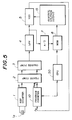
- FIG.5 a description will be given of the first embodiment of the PLL circuit according to the present invention, by referring to FIG.5.
- FIG.5 those parts which are the same as those corresponding parts in FIGS.1 and 4 are designated by the same reference numerals, and a description thereof will be omitted.
- an analog-to-digital (A/D) converter 7 is coupled between the lowpass filter 4 and the memory 8, and the output control voltage of the control voltage output circuit 15 is supplied to the VCO 5.
- a central processing unit (CPU) 50 controls the operation of the program counter 10 including the frequency dividing ratio thereof, and the write and read operations of the memory 8 including storage locations within the memory 8.
- the power source switch When the power source switch is turned ON, a plurality of input signals which may be received are successively input to the phase comparator 2. Hence, a plurality of voltage data corresponding to the input signals are successively supplied from the A/D converter 7 to the memory 8 and stored under the control of the CPU 50 which controls the write operation of the memory 8.
- the memory 8 may store data other than the voltage data, such as frequency data corresponding to the input signals.
- the CPU 50 controls the read operation of the memory 8 so as to read the voltage data corresponding to the specific input signal.
- the read voltage data is supplied to the control voltage output circuit 15 which includes a digital-to-analog (D/A) converter (not shown), and the control voltage output circuit 15 outputs a predetermined analog control voltage based on the voltage data.
- the oscillation of the VCO 5 is controlled by the predetermined analog control voltage from the control voltage output circuit 15, and the output of the VCO 5 is fed back to the phase comparator 2 via the program counter 10.
- the voltage data corresponding to this other input signal is similarly read out from the memory 8 and supplied to the control voltage output circuit 15.
- the oscillation of the VCO 5 is controlled by an analog control voltage which is output from the control voltage output circuit 15 based on the read voltage data, and the output of the VCO 5 is fed back to the phase comparator 2 via the program counter 10.
- the lock-up time can be reduced effectively because it is possible to eliminate the undesirable effects of the elements which exist in the closed loop circuit and have a time constant.
- the PLL circuit can lock to an arbitrary target frequency without being affected by the time constant of the lowpass filter 4, because the control voltage supplied to the VCO 5 is generated based on the voltage data which is read from the memory 8.
- the voltage data can be read out from the memory 8 within a short time and the lock-up time is virtually unaffected relative to the read out time.
- the power consumption of the PLL circuit can be reduced since the lock-up time can be reduced.
- the memory 8 even when the circuit characteristic of the VCO 5 and the like changes with time, the memory 8 always stores the voltage data for the present circuit characteristic. Therefore, the lock-up time can be reduced even when the circuit characteristic of the VCO 5 and the like changes with time.
- FIG.5 shows the case where the first embodiment is applied to the type of PLL circuit shown in FIG.1.
- the first embodiment can similarly be applied to the types of PLL circuits shown in FIGS.2 and 3.
- FIG.6 an operating principle of a second embodiment of the PLL circuit according to the present invention, by referring to FIG.6.
- FIG.6 those parts which are the same as those corresponding parts in FIGS.4 and 5 are designated by the same reference numerals, and a description thereof will be omitted.
- the PLL circuit includes a phase comparator 2, a lowpass filter 4, a VCO 5, a switch 6, an A/D converter 7, a memory 8 and a D/A converter 9 which are coupled as shown.
- a circuit part surrounded by a one-dot chain line is formed as a semiconductor integrated circuit (LSI chip).
- LSI chip semiconductor integrated circuit
- the switch 6 is connected to a position A when the power source switch is turned ON. For this reason, the output control voltage of the lowpass filter 4 is supplied to the A/D converter 7 via the switch 6, and an output digital control signal of the A/D converter 7 is stored in the memory 8.
- the digital control signal from the A/D converter 7 is stored for a plurality of channels of the input signal which is applied to the phase comparator 2 every time the power source switch is turned ON.
- the switch 6 After the power source switch is turned ON and the output digital control signal of the A/D converter 7 is stored in the memory 8 for all of the desired channels, the switch 6 is switched to a position B. Hence, the digital control signal read out from the memory 8 is converted into the analog control voltage in the D/A converter 9 before being supplied to the VCO 5 via the switch 6. In other words, the VCO 5 is controlled by the control voltage which is derived from the digital control signal which is stored in the memory 8 at the time when the power source switch is turned ON.
- the digital control signal is stored in the memory 8 for a plurality of channels at the time when the power source switch is turned ON, and the VCO 5 is controlled based on the digital control signal which is read out from the memory 8. Therefore, the PLL circuit can be locked to an arbitrary target frequency substantially by the time which is required to read the digital control signal from the memory 8, without being affected by the time constant of the lowpass filter 4 and the like. For this reason, the power consumption of the PLL circuit can be reduced since the lock-up time can be reduced. Furthermore, even when the circuit characteristic of the VCO 5 and the like changes with time, the memory 8 always stores the digital control signal for the present circuit characteristic. Accordingly, the lock-up time can be reduced even when the circuit characteristic of the VCO 5 and the like changes with time.
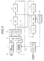
- FIG.7 those parts which are the same as those corresponding parts in FIGS.1 and 6 are designated by the same reference numerals, and a description thereof will be omitted.
- the PLL circuit includes in addition to the elements shown in FIG.1, a switch 6, an A/D converter 7, a memory 8, a D/A converter 9, a shift register 11 and an address register 12 which are coupled as shown.
- the memory 8 is a random access memory (RAM).
- the switch 6 is provided between an input end of the lowpass filter 4 and an output end of the D/A converter 9, and this switch 6 is closed after a predetermined time from the time when the power source switch is turned ON.
- the switch 6 may be closed manually or, closed automatically in response to a signal from a timer (not shown) or the like which times the predetermined time.
- a program signal corresponding to a plurality of channels which may be received is supplied to the shift register 11.
- the program signal may be received from a CPU (not shown).
- the shift register 11 generates control signals S C1 , ..., S Cn based on the program signal, and supplies the control signals S C1 , ..., S Cn to the program counter 10 and the address register 12.
- the program counter 10 frequency-divides the oscillation frequency f0 of the VCO 5 with frequency dividing ratios 1/N1, ..., 1/N n which are determined by the control signals S C1 , ..., S Cn , and successively supplies divided frequencies f0/N1, ..., f0/N n to the phase comparator 2.
- the phase comparator 2 successively generates control voltages V C1 , ..., V Cn for controlling the VCO 5 based on the divided frequencies f0/N1, ..., f0/N n .
- the control voltages V C1 , ..., V Cn are successively supplied to the A/D converter 7 via the charge pump 3 and the lowpass filter 4, and are successively converted into digital control signals and supplied to the RAM 8.
- control signals S C1 , ..., S Cn from the shift register 11 are successively supplied to the address register 12.
- the address register 12 successively inputs address signals S A1 , ..., S An to the RAM 8 in correspondence with the control signals S C1 , ..., S Cn .
- the RAM 8 Based on the address signals S A1 , ..., S An , the RAM 8 successively stores the digital signals corresponding to the control voltages V C1 , ..., V Cn .
- the switch 6 closes when the storage of all the digital signals corresponding to the control voltages V C1 , ..., V Cn ends.
- the D/A converter 9 successively converts the digital signals stored in the RAM 8 into the control voltages V C1 , ..., V Cn and supplies the control voltages V C1 , ..., V Cn to the lowpass filter 4 via the closed switch 6.
- the carrier frequency successively hops in synchronism with the change in the coded state of the code sequences which are specified by the control voltages V C1 , ..., V Cn .
- the PLL circuit successively locks to a plurality of specific frequencies based on the control voltages V C1 , ..., V C which are derived from the digital signals read from the RAM 8 based on the address signals S A1 , ..., S An .
- the time constant of the lowpass filter 4 greatly affects the lock-up time of the closed loop formed in conventional PLL circuit shown in FIG.1
- the lock-up time of this embodiment is unaffected by the time constant of the lowpass filter 4 and it is therefore possible to reduce the lock-up time compared to the conventional PLL circuit.
- the PLL circuit When the PLL circuit is to lock to a constant frequency, the PLL circuit can carry out a normal PLL operation by opening the switch 6.
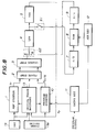
- FIG.8 a description will be given of a first modification of the second embodiment, by referring to FIG.8.
- the second embodiment is applied to the type of PLL circuit shown in FIG.3.
- FIG.8 those parts which are the same as those corresponding parts in FIGS.3 and 7 are designated by the same reference numerals, and a description thereof will be omitted.
- a first switch 61 is provided between an output end of the lowpass filter 4 and an input end of the A/D converter 7, and a second switch 62 is provided between an output end of the charge pump 3 and an input end of the lowpass filter 4.
- the first switch 61 is turned ON and the second switch 62 is switched from a position A to a position B after a predetermined time elapses from the time when the power source switch is turned ON.
- FIG.9 a description will be given of a second modification of the second embodiment, by referring to FIG.9.
- the second embodiment is applied to the type of PLL circuit shown in FIG.3.
- FIG.9 those parts which are the same as those corresponding parts in FIGS.3, 7 and 8 are designated by the same reference numerals, and a description thereof will be omitted.
- the circuit construction of this second modification is basically the same as that of the first modification.
- the first switch 61 is controlled by a write signal S W and the second switch 62 is controlled by a read signal S R .
- the read and write signals S R and S W are also supplied to the address register 12.
- the read and write signals S R and S W are output from the same CPU (not shown) which outputs the program signal which is supplied to the shift register 11.
- the address register 12 When the write signal S W is supplied to the address register 12, the address register 12 successively supplies the address signals S A1 , ..., S An to the RAM 8 in response to the write signal S W .
- the first switch 61 is closed in response to the write signal S W so that a cold start initial operation is carried out.
- the write signal S W ceases, thereby returning the first switch 61 to the open state.
- the read signal S R is supplied to the address register 12 and the second switch 62.
- the connection of the second switch 62 is switched from the position A to the position B in response to the read signal S R , and the output end of the D/A converter 9 becomes coupled to the input end of the lowpass filter 4.
- the address register 12 successively supplies the address signals S A1 , ..., S An to the RAM 8 in response to the read signal S R , and the digital signals corresponding to the control voltages V C1 , ..., V Cn are successively read out from the RAM 8 and converted into the control voltages V C1 , ..., V Cn by the D/A converter 9.
- the control voltages V C1 , ..., V Cn output from the D/A converter 9 are successively supplied to the lowpass filter 4 via the switch 62.
- control voltages V C1 , ..., V Cn successively output from the D/A converter 9 are supplied to the input end of the lowpass filter 4.
- control voltages V C1 , ..., V Cn which are successively output from the D/A converter 9 are supplied to the output end of the lowpass filter 4, that is, directly to the input end of the VCO 5.
- FIG.6 shows the operating principle of the second embodiment.
- the RAM 8 of the above described embodiments and modifications store the digital signals corresponding to the control voltages V C1 , ..., V Cn which are generated for the plurality of channels.
- the RAM 8 may of course additionally store channel information such as the station name of each channel, the frequency of each channel and the genre of each channel.
- control voltages V C1 , ..., V Cn which are derived from the digital signals read out from the RAM 8 and/or the channel information read out from the RAM 8 may be supplied to an output device (not shown).
- the output device is a display device, it is possible to display the channel information and the like read out from the RAM 8.
- the output device is a notifying means such as an indicator lamp, it is possible to notify the channel information and the like to the operator.
- switches 6, 61 and 62 are made of analog switches, it is possible to synchronize the switching operation to the read and write operations of the RAM 8 as in the case of the second modification shown in FIG.9.
- the memory 8 shown in FIG.6 is not limited to a RAM, and for example, an electrically erasable programmable read only memory (EEPROM) may be used as the memory 8.
- EEPROM electrically erasable programmable read only memory
Landscapes
- Physics & Mathematics (AREA)
- Engineering & Computer Science (AREA)
- Computer Hardware Design (AREA)
- Computing Systems (AREA)
- General Engineering & Computer Science (AREA)
- Mathematical Physics (AREA)
- Stabilization Of Oscillater, Synchronisation, Frequency Synthesizers (AREA)
- Dram (AREA)
Applications Claiming Priority (2)
| Application Number | Priority Date | Filing Date | Title |
|---|---|---|---|
| JP214102/90 | 1990-08-13 | ||
| JP2214102A JPH0496515A (ja) | 1990-08-13 | 1990-08-13 | 位相固定ループ回路及び半導体集積回路 |
Publications (1)
| Publication Number | Publication Date |
|---|---|
| EP0471502A1 true EP0471502A1 (de) | 1992-02-19 |
Family
ID=16650266
Family Applications (1)
| Application Number | Title | Priority Date | Filing Date |
|---|---|---|---|
| EP91307248A Withdrawn EP0471502A1 (de) | 1990-08-13 | 1991-08-07 | Phasenregelschaltung und integrierte Halbleiterschaltung dafür |
Country Status (3)
| Country | Link |
|---|---|
| EP (1) | EP0471502A1 (de) |
| JP (1) | JPH0496515A (de) |
| KR (1) | KR920005495A (de) |
Cited By (9)
| Publication number | Priority date | Publication date | Assignee | Title |
|---|---|---|---|---|
| EP0579978A1 (de) * | 1992-06-29 | 1994-01-26 | Nec Corporation | Frequenzsynthesierer |
| DE19631113A1 (de) * | 1995-09-06 | 1997-03-13 | Samsung Electronics Co Ltd | Einzelphasenregelschleifenschaltung und Verfahren zur Verbesserung der Phasensynchronisationszeit |
| DE19653134A1 (de) * | 1995-12-29 | 1997-11-06 | Samsung Electronics Co Ltd | PLL-Schaltung zur Verbesserung der Phasensynchronisierungszeit |
| US5926515A (en) * | 1995-12-26 | 1999-07-20 | Samsung Electronics Co., Ltd. | Phase locked loop for improving a phase locking time |
| DE19906561A1 (de) * | 1999-02-17 | 2000-09-14 | Dosch & Amand Gmbh & Co Kg | Phasenregelkreis |
| WO2001061857A3 (en) * | 2000-02-18 | 2002-01-31 | Ericsson Inc | Method and apparatus for tuning an oscillator to a selected frequency |
| DE19654935C2 (de) * | 1995-02-06 | 2002-06-13 | Mitsubishi Electric Corp | Halbleitereinrichtung |
| US6414535B1 (en) | 1995-02-06 | 2002-07-02 | Mitsubishi Denki Kabushiki Kaisha | Semiconductor device realizing internal operational factor corresponding to an external operational factor stably regardless of fluctuation of external operational factor |
| US7545222B2 (en) | 2006-01-06 | 2009-06-09 | Realtek Semiconductor Corp. | Phase lock loop for rapid lock-in and method therefor |
Families Citing this family (4)
| Publication number | Priority date | Publication date | Assignee | Title |
|---|---|---|---|---|
| JP4127208B2 (ja) | 2003-07-14 | 2008-07-30 | 日本電気株式会社 | 周波数シンセサイザ |
| JP2007027981A (ja) | 2005-07-13 | 2007-02-01 | Futaba Corp | 発振装置およびその制御方法 |
| WO2012001846A1 (ja) * | 2010-06-28 | 2012-01-05 | パナソニック株式会社 | 基準周波数生成回路、半導体集積回路、電子機器 |
| JP5670123B2 (ja) * | 2010-08-20 | 2015-02-18 | 富士通株式会社 | Pllシンセサイザ |
Citations (3)
| Publication number | Priority date | Publication date | Assignee | Title |
|---|---|---|---|---|
| EP0041882A1 (de) * | 1980-06-03 | 1981-12-16 | Thomson-Csf | Einrichtung zum Voreinstellen der Frequenz einer indirekten Frequenzsyntheseschaltung und eine solche Einrichtung enthaltende Frequenzsyntheseschaltung |
| US4410860A (en) * | 1980-12-31 | 1983-10-18 | Rca Corporation | Frequency synthesizer with learning circuit |
| FR2535545A1 (fr) * | 1982-10-29 | 1984-05-04 | Thomson Csf | Synthetiseur a temps d'acquisition rapide de frequence et systeme de transmission radioelectrique a saut de frequence comportant un tel synthetiseur |
-
1990
- 1990-08-13 JP JP2214102A patent/JPH0496515A/ja active Pending
-
1991
- 1991-08-07 EP EP91307248A patent/EP0471502A1/de not_active Withdrawn
- 1991-08-13 KR KR1019910013971A patent/KR920005495A/ko not_active Abandoned
Patent Citations (3)
| Publication number | Priority date | Publication date | Assignee | Title |
|---|---|---|---|---|
| EP0041882A1 (de) * | 1980-06-03 | 1981-12-16 | Thomson-Csf | Einrichtung zum Voreinstellen der Frequenz einer indirekten Frequenzsyntheseschaltung und eine solche Einrichtung enthaltende Frequenzsyntheseschaltung |
| US4410860A (en) * | 1980-12-31 | 1983-10-18 | Rca Corporation | Frequency synthesizer with learning circuit |
| FR2535545A1 (fr) * | 1982-10-29 | 1984-05-04 | Thomson Csf | Synthetiseur a temps d'acquisition rapide de frequence et systeme de transmission radioelectrique a saut de frequence comportant un tel synthetiseur |
Non-Patent Citations (1)
| Title |
|---|
| 37TH IEEE VEHICULAR TECHNOLOGY CONFERENCE 1 June 1987, TAMPA, FLORIDA,US pages 435 - 440; JUN'ICHI NAKAGAWA ET AL.: 'HANDHELD TELEPHONE FOR 800 MHz-BAND CELLULAR RADIO SYSTEMS' * |
Cited By (14)
| Publication number | Priority date | Publication date | Assignee | Title |
|---|---|---|---|---|
| US5379002A (en) * | 1992-06-29 | 1995-01-03 | Nec Corporation | Frequency synthesizer using intermittently controlled phase locked loop |
| AU663838B2 (en) * | 1992-06-29 | 1995-10-19 | Nec Corporation | Frequency synthesizer using intermittently controlled phase locked loop |
| EP0579978A1 (de) * | 1992-06-29 | 1994-01-26 | Nec Corporation | Frequenzsynthesierer |
| DE19654935C2 (de) * | 1995-02-06 | 2002-06-13 | Mitsubishi Electric Corp | Halbleitereinrichtung |
| US6414535B1 (en) | 1995-02-06 | 2002-07-02 | Mitsubishi Denki Kabushiki Kaisha | Semiconductor device realizing internal operational factor corresponding to an external operational factor stably regardless of fluctuation of external operational factor |
| DE19631113A1 (de) * | 1995-09-06 | 1997-03-13 | Samsung Electronics Co Ltd | Einzelphasenregelschleifenschaltung und Verfahren zur Verbesserung der Phasensynchronisationszeit |
| US5926515A (en) * | 1995-12-26 | 1999-07-20 | Samsung Electronics Co., Ltd. | Phase locked loop for improving a phase locking time |
| DE19653134C2 (de) * | 1995-12-29 | 1999-02-18 | Samsung Electronics Co Ltd | Phasenregelschleife |
| DE19653134A1 (de) * | 1995-12-29 | 1997-11-06 | Samsung Electronics Co Ltd | PLL-Schaltung zur Verbesserung der Phasensynchronisierungszeit |
| DE19906561A1 (de) * | 1999-02-17 | 2000-09-14 | Dosch & Amand Gmbh & Co Kg | Phasenregelkreis |
| EP1030452A3 (de) * | 1999-02-17 | 2003-10-29 | Dosch & Amand GmbH & Co. KG | Phasenregelkreis |
| DE19906561B4 (de) * | 1999-02-17 | 2005-08-25 | Dosch & Amand Gmbh & Co. Kg | Phasenregelkreis |
| WO2001061857A3 (en) * | 2000-02-18 | 2002-01-31 | Ericsson Inc | Method and apparatus for tuning an oscillator to a selected frequency |
| US7545222B2 (en) | 2006-01-06 | 2009-06-09 | Realtek Semiconductor Corp. | Phase lock loop for rapid lock-in and method therefor |
Also Published As
| Publication number | Publication date |
|---|---|
| KR920005495A (ko) | 1992-03-28 |
| JPH0496515A (ja) | 1992-03-27 |
Similar Documents
| Publication | Publication Date | Title |
|---|---|---|
| US5629651A (en) | Phase lock loop having a reduced synchronization transfer period | |
| EP0471502A1 (de) | Phasenregelschaltung und integrierte Halbleiterschaltung dafür | |
| US4577163A (en) | Digital phase locked loop | |
| EP1006662A2 (de) | Integrierte Halbleiterschaltung | |
| US6564040B1 (en) | Communication device and communication method | |
| US5757216A (en) | Electronic device using phase synchronous circuit | |
| EP0499245A2 (de) | Synthesizer mit einem Phasenregelkreis für die Verwendung in einem Zeitmultiplexkommunikationssystem | |
| EP1246369A2 (de) | Verfahren zum Umschalten der Betriebsart einer PLL-Schaltung und Schaltung zur Steuerung der Betriebsart einer PLL-Schaltung | |
| US5727019A (en) | Digital modem | |
| US5892405A (en) | PLL synthesizer apparatus | |
| US5578968A (en) | Frequency converter, multistage frequency converter and frequency synthesizer utilizing them | |
| KR960000809B1 (ko) | Pll 합성회로 | |
| US5907590A (en) | Frequency dividing circuit, frequency dividing method and telephone terminal device incorporating the frequency dividing circuit | |
| US5399985A (en) | Digital PLL circuit | |
| US6795516B1 (en) | Reset circuit and pll frequency synthesizer | |
| GB2236922A (en) | Frequency synthesisers | |
| US5656958A (en) | Frequency synthesizing device | |
| EP0881775A1 (de) | Taktgenerator | |
| US6094100A (en) | PLL synthesizer apparatus | |
| KR0138024B1 (ko) | 아이디이 인터페이스 장치 | |
| KR100382640B1 (ko) | 고속으로동기하는위상동기루프(pll)장치및방법 | |
| JP2697322B2 (ja) | 位相同期回路 | |
| EP0618682B1 (de) | Frequenzsynthetisierer | |
| JPH0541664A (ja) | 周波数シンセサイザ | |
| KR970005394B1 (ko) | 혼합형 주파수 합성기(Hybrid Frequency Synthesizer) |
Legal Events
| Date | Code | Title | Description |
|---|---|---|---|
| PUAI | Public reference made under article 153(3) epc to a published international application that has entered the european phase |
Free format text: ORIGINAL CODE: 0009012 |
|
| AK | Designated contracting states |
Kind code of ref document: A1 Designated state(s): DE FR GB |
|
| 17P | Request for examination filed |
Effective date: 19920225 |
|
| 17Q | First examination report despatched |
Effective date: 19920525 |
|
| STAA | Information on the status of an ep patent application or granted ep patent |
Free format text: STATUS: THE APPLICATION IS DEEMED TO BE WITHDRAWN |
|
| 18D | Application deemed to be withdrawn |
Effective date: 19931012 |