EP0472408A2 - Système de communication ATM - Google Patents
Système de communication ATM Download PDFInfo
- Publication number
- EP0472408A2 EP0472408A2 EP91307669A EP91307669A EP0472408A2 EP 0472408 A2 EP0472408 A2 EP 0472408A2 EP 91307669 A EP91307669 A EP 91307669A EP 91307669 A EP91307669 A EP 91307669A EP 0472408 A2 EP0472408 A2 EP 0472408A2
- Authority
- EP
- European Patent Office
- Prior art keywords
- cell
- function means
- information
- vci
- cells
- Prior art date
- Legal status (The legal status is an assumption and is not a legal conclusion. Google has not performed a legal analysis and makes no representation as to the accuracy of the status listed.)
- Granted
Links
Images


Classifications
-
- H—ELECTRICITY
- H04—ELECTRIC COMMUNICATION TECHNIQUE
- H04L—TRANSMISSION OF DIGITAL INFORMATION, e.g. TELEGRAPHIC COMMUNICATION
- H04L49/00—Packet switching elements
- H04L49/55—Prevention, detection or correction of errors
- H04L49/557—Error correction, e.g. fault recovery or fault tolerance
-
- H—ELECTRICITY
- H04—ELECTRIC COMMUNICATION TECHNIQUE
- H04L—TRANSMISSION OF DIGITAL INFORMATION, e.g. TELEGRAPHIC COMMUNICATION
- H04L12/00—Data switching networks
- H04L12/54—Store-and-forward switching systems
- H04L12/56—Packet switching systems
- H04L12/5601—Transfer mode dependent, e.g. ATM
- H04L12/5602—Bandwidth control in ATM Networks, e.g. leaky bucket
-
- H—ELECTRICITY
- H04—ELECTRIC COMMUNICATION TECHNIQUE
- H04L—TRANSMISSION OF DIGITAL INFORMATION, e.g. TELEGRAPHIC COMMUNICATION
- H04L49/00—Packet switching elements
- H04L49/20—Support for services
-
- H—ELECTRICITY
- H04—ELECTRIC COMMUNICATION TECHNIQUE
- H04L—TRANSMISSION OF DIGITAL INFORMATION, e.g. TELEGRAPHIC COMMUNICATION
- H04L49/00—Packet switching elements
- H04L49/25—Routing or path finding in a switch fabric
- H04L49/253—Routing or path finding in a switch fabric using establishment or release of connections between ports
- H04L49/255—Control mechanisms for ATM switching fabrics
-
- H—ELECTRICITY
- H04—ELECTRIC COMMUNICATION TECHNIQUE
- H04L—TRANSMISSION OF DIGITAL INFORMATION, e.g. TELEGRAPHIC COMMUNICATION
- H04L49/00—Packet switching elements
- H04L49/30—Peripheral units, e.g. input or output ports
- H04L49/3009—Header conversion, routing tables or routing tags
-
- H—ELECTRICITY
- H04—ELECTRIC COMMUNICATION TECHNIQUE
- H04L—TRANSMISSION OF DIGITAL INFORMATION, e.g. TELEGRAPHIC COMMUNICATION
- H04L49/00—Packet switching elements
- H04L49/30—Peripheral units, e.g. input or output ports
- H04L49/3081—ATM peripheral units, e.g. policing, insertion or extraction
- H04L49/309—Header conversion, routing tables or routing tags
-
- H—ELECTRICITY
- H04—ELECTRIC COMMUNICATION TECHNIQUE
- H04L—TRANSMISSION OF DIGITAL INFORMATION, e.g. TELEGRAPHIC COMMUNICATION
- H04L49/00—Packet switching elements
- H04L49/50—Overload detection or protection within a single switching element
- H04L49/501—Overload detection
- H04L49/503—Policing
-
- H—ELECTRICITY
- H04—ELECTRIC COMMUNICATION TECHNIQUE
- H04L—TRANSMISSION OF DIGITAL INFORMATION, e.g. TELEGRAPHIC COMMUNICATION
- H04L49/00—Packet switching elements
- H04L49/55—Prevention, detection or correction of errors
- H04L49/552—Prevention, detection or correction of errors by ensuring the integrity of packets received through redundant connections
-
- H—ELECTRICITY
- H04—ELECTRIC COMMUNICATION TECHNIQUE
- H04L—TRANSMISSION OF DIGITAL INFORMATION, e.g. TELEGRAPHIC COMMUNICATION
- H04L49/00—Packet switching elements
- H04L49/55—Prevention, detection or correction of errors
- H04L49/555—Error detection
-
- H—ELECTRICITY
- H04—ELECTRIC COMMUNICATION TECHNIQUE
- H04L—TRANSMISSION OF DIGITAL INFORMATION, e.g. TELEGRAPHIC COMMUNICATION
- H04L12/00—Data switching networks
- H04L12/54—Store-and-forward switching systems
- H04L12/56—Packet switching systems
- H04L12/5601—Transfer mode dependent, e.g. ATM
- H04L2012/5625—Operations, administration and maintenance [OAM]
-
- H—ELECTRICITY
- H04—ELECTRIC COMMUNICATION TECHNIQUE
- H04L—TRANSMISSION OF DIGITAL INFORMATION, e.g. TELEGRAPHIC COMMUNICATION
- H04L12/00—Data switching networks
- H04L12/54—Store-and-forward switching systems
- H04L12/56—Packet switching systems
- H04L12/5601—Transfer mode dependent, e.g. ATM
- H04L2012/5629—Admission control
- H04L2012/5631—Resource management and allocation
- H04L2012/5636—Monitoring or policing, e.g. compliance with allocated rate, corrective actions
- H04L2012/5637—Leaky Buckets
-
- H—ELECTRICITY
- H04—ELECTRIC COMMUNICATION TECHNIQUE
- H04L—TRANSMISSION OF DIGITAL INFORMATION, e.g. TELEGRAPHIC COMMUNICATION
- H04L12/00—Data switching networks
- H04L12/54—Store-and-forward switching systems
- H04L12/56—Packet switching systems
- H04L12/5601—Transfer mode dependent, e.g. ATM
- H04L2012/5638—Services, e.g. multimedia, GOS, QOS
- H04L2012/5646—Cell characteristics, e.g. loss, delay, jitter, sequence integrity
- H04L2012/5647—Cell loss
-
- H—ELECTRICITY
- H04—ELECTRIC COMMUNICATION TECHNIQUE
- H04L—TRANSMISSION OF DIGITAL INFORMATION, e.g. TELEGRAPHIC COMMUNICATION
- H04L12/00—Data switching networks
- H04L12/54—Store-and-forward switching systems
- H04L12/56—Packet switching systems
- H04L12/5601—Transfer mode dependent, e.g. ATM
- H04L2012/5638—Services, e.g. multimedia, GOS, QOS
- H04L2012/5646—Cell characteristics, e.g. loss, delay, jitter, sequence integrity
- H04L2012/5649—Cell delay or jitter
-
- H—ELECTRICITY
- H04—ELECTRIC COMMUNICATION TECHNIQUE
- H04L—TRANSMISSION OF DIGITAL INFORMATION, e.g. TELEGRAPHIC COMMUNICATION
- H04L12/00—Data switching networks
- H04L12/54—Store-and-forward switching systems
- H04L12/56—Packet switching systems
- H04L12/5601—Transfer mode dependent, e.g. ATM
- H04L2012/5638—Services, e.g. multimedia, GOS, QOS
- H04L2012/5646—Cell characteristics, e.g. loss, delay, jitter, sequence integrity
- H04L2012/5651—Priority, marking, classes
-
- H—ELECTRICITY
- H04—ELECTRIC COMMUNICATION TECHNIQUE
- H04L—TRANSMISSION OF DIGITAL INFORMATION, e.g. TELEGRAPHIC COMMUNICATION
- H04L12/00—Data switching networks
- H04L12/54—Store-and-forward switching systems
- H04L12/56—Packet switching systems
- H04L12/5601—Transfer mode dependent, e.g. ATM
- H04L2012/5678—Traffic aspects, e.g. arbitration, load balancing, smoothing, buffer management
- H04L2012/568—Load balancing, smoothing or shaping
-
- H—ELECTRICITY
- H04—ELECTRIC COMMUNICATION TECHNIQUE
- H04L—TRANSMISSION OF DIGITAL INFORMATION, e.g. TELEGRAPHIC COMMUNICATION
- H04L49/00—Packet switching elements
- H04L49/10—Packet switching elements characterised by the switching fabric construction
- H04L49/103—Packet switching elements characterised by the switching fabric construction using a shared central buffer; using a shared memory
-
- H—ELECTRICITY
- H04—ELECTRIC COMMUNICATION TECHNIQUE
- H04L—TRANSMISSION OF DIGITAL INFORMATION, e.g. TELEGRAPHIC COMMUNICATION
- H04L49/00—Packet switching elements
- H04L49/30—Peripheral units, e.g. input or output ports
Definitions
- the present invention relates to an ATM (Asynchronous Transfer Mode) communication system for communicating and switching user information and, more particularly, to an ATM communication system having a cell processing function of effectively performing various processing operations of a cell communicated through an ATM network.
- ATM Asynchronous Transfer Mode
- ATM Asynchronous Transfer Mode
- VC virtual channel
- VPs virtual passes
- Standard specifications of the VCs and VPs are predetermined by the CCITT (International Cord and Telephone Consultative Committee), and when an ATM communication system is realized, information communications must be controlled to meet these specifications. For example, a cell flow is observed so that a flow of cells carrying information falls within a bandwidth determined as a VP, and various processing control operations for cells such as control for discarding an overflow cell, must be performed.
- the standard format of a cell is defined to some extent by the CCITT. However, how to reliably seize asynchronously transmitted cells and how to perform this processing control pose problems.
- the ATM communication system is realized by the following architecture.
- a node system for switching a VC (Virtual Channel) set between terminal stations, and a link system for switching a VP (Virtual Path) bandling a lot of VCs are defined.
- a transmission network is constructed by connecting the link systems by means of the transmission line.
- the topology of the transmission network may be, for example, a star topology or a ring topology.
- the topology of the transmission network is determined by a trade-off between an traffic on the transmission network and a cost required for constructing a transmission network.
- the node system is connected to the transmission network for multiplexing the VC from the terminal station to the VP set on the transmission network or for separating the VCs within the VP and transiting those to another VP.
- the VP used in the link system is semi-fixedly set in accordance with instruction from an operation center.
- the VC used in the node system is dynamically set-up and released by call setup/release request from the terminal station.
- node system there are a node system for a public network being an arrangement for carriers and a node system for a private network used when a subscriber constructs another communication network, using a public network.
- the ATM network is constructed by a link system, a node system for a public network, and a node system for a private network. It is required for realizing the ATM network with a low cost that an architecture for cell processing function is constructed so as to be able to flexibly accommodate an arrangement of different polishing/shaping functions for each of the above node systems, reliability request, etc.
- the feature of the present invention is to be able to select a function wherein an ATM communication system performs, as a cell processing function in an ATM network, shaping of a cell flow output from a cell processing function unit in units of VCs so as to satisfy predetermined traffic characteristics, and the other function wherein the cell shaping is independently executed for the VC and a VP as a bundle of VCs.
- delay control for a cell is executed by only an output buffer for an ATM switch, and discard control for the cell is executed by only an input buffer for the ATM switch.
- transformation processing for transforming a logical identifier into a physical identifier can be easily and efficiently performed using an associative memory.
- each cell processing function in the ATM network has a function of inserting a management cell having a preset level in the ATM network, and a function for discriminating the level of the management cell communicated through the ATM network, and dropping or looping back the management cell in accordance with the level of the corresponding cell processing function in the ATM network.
- the management cell having the preset level is properly used, various functions in the ATM network can be tested.
- each cell processing function in the ATM network has a function of generating an alarm cell according to a malfunction position. For example, when a malfunction occurs in a former-stage section of the cell processing function, a tagging function of the corresponding cell processing function is used to generate an alarm cell. When a malfunction occurs in the entire cell processing function, a tagging function of another cell processing function to which a cell is transferred from the corresponding cell processing function via an ATM exchanger is used to generate an alarm cell. When a malfunction occurs in a node system of the ATM network, a tagging function of a cell processing function opposing the corresponding node system is used to generate an alarm cell.
- polishing for a cell flow is divided into low-speed polishing and high-speed polishing, and these polishing operations are executed independently of each other.
- this invention has a feature capable of avoiding quickly a malfunction, using the loop-back function.
- the present invention can be select a shaping for a cell flow output from a given cell processing function in units of VCs or an independent shaping for VCs and VPs, to satisfy predetermined traffic characteristics. Therefore, even if the traffic of a plurality of cells passing through the various points of the ATM network is abruptly increased accidentally due to some cause, the traffic is averaged by shaping. As a result, even when polishing control for observing a cell flow at the corresponding ATM exchanger and discarding a cell which violates the predetermined traffic characteristics is performed, the cells of the cell flow can be prevented from being unexpectedly discharged partially.
- Delay control for controlling shaping of a cell flow is performed by an output buffer for the ATM switch, and discharge control of a cell flow is executed by an input buffer for the ATM switch. Therefore, the hardware arrangement can be simplified significantly.
- a logical identifier for a VC or VP necessary for ATM switching a cell flow is transformed into a physical identifier using an associative memory. Therefore, the number of hardware components for the logical/physical transformation can be sufficiently decreased, and the transformation processing can be easily performed.
- a management cell having a preset level is sent onto the ATM network, and each cell processing function in the ATM network has a function of dropping/looping back the management cell according to its position. Therefore, various functions in the ATM network can be effectively tested according to the level of the management cell.
- Each cell processing function has a function of generating an alarm cell according to a malfunction position in the ATM network. Therefore, a malfunction condition can be effectively informed to the respective sections in the ATM network.
- this invention provides a cell processing function capable of applying to a link system to be have a high reliability, by virtue of a quick avoidance of malfunction using the loop back function.
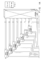
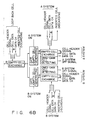
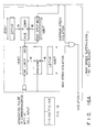
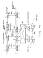
- Figs. 1A and 1B show a block diagram showing an arrangement of a node system for a public network which applies the present invention.
- An ATM switch (ATMSW; Asynchronous Transfer mode Switch) executes switching cells, which are short and fix length pocket via an ATM network.
- ATMSW Asynchronous Transfer mode Switch
- the cell switching processing is executed by the ATMSW subjecting the cell to a self-routing in accordance with the routing tag attached to the cell.
- the cell switching processing is observed by an ASP (ATMSW Processor).
- the ATMSW is connected to a user-network interface (BUNI; Boardband User-Network Interface), a network interface (BNNI; Broadband Network-Network Interface), and the like.
- BUNI Boardband User-Network Interface
- BNNI Broadband Network-Network Interface
- the ATMSW is connected to an NUNI (Narrowband User Network Interface), an NNNI (Narrowband Network-Network Interface), a VLFS (Connectionless Support Facility), a VVTT (Voice/Video Talkie Trunk), and a VVCB (Voice/Video Conference Bridge). Operations of circuit functions of these interfaces are controlled by corresponding special-purpose processors.
- a signaling cell input to a cell processing 2unction of, e.g., the BUNI or BNNI is modified into an SW cell, and a routing tag necessary for reaching an output port connected to a signaling cell switch SCSW, and a number corresponding to a signaling processor array (SPA) for processing the signaling cell are added to the SW cell.
- a signaling processor array SPA
- the ATMSW refers to routing tags added by the cell processing functions, and temporarily concentrates the signaling cells transferred from the cell processing functions to the output port connected to the SCSW. Upon reception of these cells, the SCSW refers to the SPA numbers added to the respective signaling cells, and switches the cells to the SPAs for processing the corresponding signaling cells.
- a signaling cell output from each SPA is added with a routing tag necessary for reaching an output port of the ATMSW from which the signaling cell is to be output, and is concentrated by the SCSW.
- the concentrated cells are transferred to the ATMSW.
- a signaling VC is identified by a VPI, a VCI, and a routing tag.
- the ATMSW refers to the routing tags added to the respective signaling cells, and outputs the cells to the corresponding output ports from which these cells are to be output. Thereafter, cells output from the ATMSW are subjected to predetermined processing by the cell processing function, and are output to a link.
- the cell processing function according to the present invention is a function corresponding to the above-mentioned BUNI or BNNI, and is a function of efficiently executing various processing operations for cells subjected to switching communications by the ATMSW by a simple hardware arrangement.
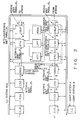
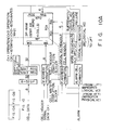
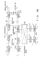
- Fig. 2 shows the overall arrangement of a typical cell processing function represented by the BUNI or BNNI.
- the BUNI or BNNI is realized on the basis of the arrangement shown in Fig. 2.
- information to be processed is temporarily adapted to a 150-Mbps cell flow, and thereafter, is interfaced with the ATMSW on the basis of the arrangement shown in Fig. 2.
- Optical data input to the cell processing function via a transmission path consisting of an optical fiber is converted into electrical data by an OUR (Optical Unit Receiver). At this time, a bit clock is simultaneously reproduced. Note that data output from the OUR is 155.52-Mbps serial data.
- An electrical signal output from the OUR is input to an FDA (Frame Disassembler) to achieve frame synchronization.
- the frame-synchronized data is serial/parallel-converted, and an 8-bit parallel signal is output as an ATM cell region signal.
- data output from the FDA is converted to 8-bit parallel data of 18.72 Mbyte/Sec in accordance with the capacity of VC-4 in an STM (Synchronous Transfer Mode)-n.
- Data is transmitted from the OUR in synchronism with the bit clock reproduced by the OUR.
- data is output from the FDA in synchronism with an 18.72-MHz clock generated by a timing supply unit.
- the FDA also has a bitrate changing function.
- the FDA also has a function of forming transmission path alarm signal by referring to an SOH (Section Over Head) or POH (Path Over Head), and informing it to an ILC (INF Local Controller) in addition to the frame synchronization and serial/parallel conversion functions.
- SOH Section Over Head
- POH Pulth Over Head
- ILC INF Local Controller
- information sent through a DCC is also informed to the ILC.
- DCC Data Communication Channel
- the ILC is a generic name for controllers (processors) such as a BUNIP, BNNIP, and the like, which perform local control of the cell processing function.
- 8-bit parallel data output from the FDA is input to a CSD (Cell Synchronizer/Information Descrambler), and cell synchronization is achieved by an HEC (Header Error Control) calculation.
- a header display signal is added to the 8-bit parallel data flow.
- the header display signal is active, a cell header octet is displayed.
- the cell-synchronized parallel data is input to an RTA (Routing Tag Adder) via an OMDI (OAM Cell Drop/Insert).
- the RTA temporarily stores an input cell, and transforms a VPI/VCI in accordance with the content of an HTT (Header Transformation Table). Furthermore, the RTA adds additional information such as information (routing tag) used in routing inside the ATMSW to the cell, and outputs the cell to an IBUF (Input Buffer).
- IBUF Input Buffer
- transformation from the VPI/VCI into a physical VCI actually used as an entry number of the HTT is performed by an LPT (Logical VCI/Physical VCI transformer), as will be described later.
- LPT Logical VCI/Physical VCI transformer
- the additional information has a 74-bit length.
- the length of the additional data added by the RTA is set to be, e.g., 88 bits in consideration of future expansion.
- a cell to be processed in this system has a 64-byte length.
- the OMDI drops/inserts OAM cells.
- An OAM cell dropped by the OMDI is transferred to the ILC in the form of a cell.
- an OAM cell to be inserted is also transferred from the ILC to the OMDI in the form of a cell.
- the OMDI and the RTA are periodically operated with a cycle of the cell length.
- the operation of the CSD does not always have a cycle of the cell length. That is, a HUNT state may be inserted in a cell synchronization establishment sequence by the HEC calculation. For this reason, cell synchronization must be established between the operation cycle of the CSD and the operation cycle of the OMDI/RTA.
- This cell synchronization is realized by arranging a buffer corresponding to two cell lengths to an output unit of the CSD. Note that the CSD keeps outputting empty cells to the OMDI during a period in which cell synchronization is not established.
- a cell transfer operation and cell input/output operation in the CSD/OMDI/RTA are assumed to be performed in an 8-bit parallel format.
- a cell output operation from the RTA is assumed to be performed at 149.76 Mbps x (64/53) since the cell length is increased.
- the cell input/output operation of the CSD, the cell input/output operation of the OMDI, and the cell input operation of the RTA are performed in synchronism with a clock of, e.g., 18.72 MHz (2.83 ⁇ sec per cell), and the cell output operation of the RTA is performed in synchronism with a clock of, e.g., 18.72 x (64/53) MHz.
- a traffic of a cell flow is observed as follows when a routing tag is added by the RTA.
- a traffic carried by each VC is observed by a TOVA (Traffic Observer/Violation Tag Adder). Basically, this traffic measurement is performed by observing an access to the HTT for the purpose of VPI/VCI transformation. As a result of the traffic measurement, the TOVA instructs the RTA to add a violation tag to a cell which is determined to exceed a capacity assigned to a given VC. Thus, VC polishing for each VC is performed. The position of the violation tag is set, e.g., inside the additional information of a cell.
- a newly generated VC is set in such a manner that a VPI/VCI at an input-side link of the VC, a physical VCI corresponding to the set of the VPI/VCI, a VPI/VCI at an output-side link, and a routing tag for designating a path for the VC in the ATMSW are informed from the ILC to the HTT and the LPT, and several parameters for setting the capacity of the VC are informed from the ILC to the TOVA.
- the HTT and TOVA which received the above-mentioned parameters from the ILC receive the parameters, and control a cell flow in accordance with the parameters.
- a cell output from the RTA is temporarily stored in the IBUF, and is output in correspondence with an operation speed of the ATMSW. Cell discard processing (to be described later) is performed by only the IBUF, and a cell with a violation tag is always discarded by the IBUF.
- a cell output from the IBUF is transferred to the ATMSW.
- the ATMSW refers to a routing tag of the additional information added to each cell by the RTA, and transfers the cell to an output port requesting it.
- a cell transfer operation is performed at the same rate as the output rate of the IBUF.
- a cell output from the output port of the ATMSW is input to an OBUF (Output Buffer), and is temporarily stored therein.
- the OBUF outputs the cell in correspondence with a rate in the next section. More specifically, a cell input operation to the OBUF is performed at the same rate as the cell output rate from the IBUF. In contrast to this, a cell transfer operation from the OBUF to an RTD (Routing Tag Deleter) is performed at 149.76 Mbps x (64/53), as will be described later. Therefore, a stay of cells inside a buffer due to conflicts associated with output ports mainly occurs in the OBUF.
- the OBUF performs cell delay class control.
- the cell delay class control in the OBUF can be considered as a delay class control scheme executed on the basis of the concept in that if cells stay inside the system, most of the cells stay in the OBUF since the cell transfer rate of the ATMSW is increased, as described above.
- a cell output from the OBUF is input to a CSH (Cell Sharer).
- CSH Cell Sharer
- an output cell flow is observed by a leaky bucket, and shaping processing for the cell flow is performed.
- This shaping processing an output operation of the cell is controlled so as not to be determined by a polishing function in the opposing cell processing function that a transmission output cell is a violation cell.
- the cell input/output rate in the CSH is equal to the cell output rate in the OBUF.
- a cell output from the CSH is input to the RTD (Routing Tag Deleter).
- the cell is input to the RTD at a rate of 149.76 Mbps x (64/53), thereby preventing buffers for deleting the above-mentioned additional information included in the RTD from overflowing. Note that the cell is input to the RTD in an 8-bit parallel format.
- a cell output from the RTD is input to a CIS (Cell Information Scrambler) via another OMDI.
- the CIS scrambles an information portion of the cell.
- a data input/output signal of the OMDI/CIS is processed as an 18.72-MHz 8-bit parallel signal.
- the cell scrambled by the CIS is input to an FAS (Frame Assembler), and is added with an SOH and a POH to be transformed into an STM frame. Thereafter, the cell is parallel/serial-converted.
- a byte phase of a cell in an ATM region is aligned with an intra-payload position indicated by an AU-4 pointer.
- management information to be carried by the SOH and POH is informed from the ILC to the FAS, and at the same time, information to be carried in a DCC channel is informed from the ILC to the FAS.
- the FAS outputs the STM frame as a serial signal.
- a cell header in a payload may be indicated by an H4 pointer of the VC-4 according to the consultation of the CCITT. If the cell header in the payload is indicated using the H4 pointer of the VC-4, a cell header signal can be in parallel provided to 8-bit parallel data like in other portions, and an interface among function elements can be standardized.
- the STM frame output from the FAS is transferred to an OUS (OPT Unit Sender), is subjected to electrooptical conversion by the OUS, and an optical signal is then output onto an optical fiber.
- OUS OPT Unit Sender
- fault detection in this system is performed as follows.
- the OUR, OUS, FDA, CSD, and OBUF can supervise a receiving off (REC) signal based on their inputs.
- the FDA can supervise its own states associated with frame synchronization, i.e., HUNT, SYNCH, and PRESYNC states
- the CSD can supervise its own states associated with cell synchronization, i.e., HUNT, SYNCH, and PRESYNC states.
- the above-mentioned cell processing function is used in a large-scale ATM switch, it is preferable to detect an increase in bit error rate of the IBUF-ATMSW-OBUF path.
- a parity bit of a cell is assigned in one byte in additional information to be added to the cell by the RTA.
- the parity bit is checked by the RTD, a decrease in bit error characteristics of the IBUF-ATMSW-OBUF path can be supervised.
- fault detection is performed by the following scheme.
- This fault detection is performed when a new VC is set, and is executed to confirm that a path for the VC is normal. More specifically, the fault detection is performed in such a manner that after necessary data is written in the HTT/LPT upon setting of a VC, an OAM cell is caused to pass from the ILC via the ODMI, and it is checked if the OAM cell is detected by the OMDI at the output side of the VC.
- the same operation is performed in an ATM link system accommodating subscribers, and between adjacent ATM node systems. For this reason, an OAM cell is looped back in the subscriber accommodating link system, and between the adjacent ATM node systems. Loop back control of the OAM cell can be realized by transferring a loop back OAM cell from the OMDI arranged between the CSD and the RTA in each cell processing function to another OMDI arranged between the RTD and the CIS.
- Fault detection of the TOVA is realized by conforming, upon setting of a VC, if a polishing algorithm is operated correctly, as will be described later.
- Fault detection of the CSH is also realized by placing an output restriction on a cell using the polishing algorithm like in the fault detection of the TOVA, as will be described later.
- the fault detection of the CSH is performed by confirming, upon setting of a new VC, if the polishing algorithm is operated correctly, like in the TOVA, and confirming if an output restriction is placed. This fault detection will be described in detail later.
- discard class control and delay class control are performed. Fault detection in the discard class control is realized by analyzing a cell discarded by the IBUF in the ILC.
- the IBUF informs, to the ILC, the discarded cell itself, and the numbers of cells in units of discard classes held in the IBUF when the cell is discarded. Every time a cell is discarded, the ILC confirms, on the basis of the numbers of cells in units of discard classes in the IBUF, and a discard class to which the discarded cell belongs, that the discard class control is normally operated.
- the OBUF has counters for counting the numbers of cells held therein in correspondence with delay classes. Every time a cell is output, the OBUF compares the numbers of cells in units of classes, and a delay class of the cell actually output from the OBUF, thereby checking if a delay control algorithm is normally operated. If an abnormality is found in the checking processing, the OBUF informs this to the ILC.
- fault detection of the ILC is performed by a conventional scheme, e.g., runaway check using a watch-dog timer, and existence checking via periodical communications between the ILC and a supervision controller.
- FDA/FAS is a framer/deframer for STM-1.
- the construction method for this is well-known, therefore more detail description is not added here.
- the cell synchronization function and the scramble/descramble function are supported by the CSD (Cell Synchronizer/Information Descrambler) and the CIS (Cell Information Scrambler) in the general arrangement of the cell processing function shown in Fig. 2.
- CSD Cell Synchronizer/Information Descrambler
- CIS Cell Information Scrambler
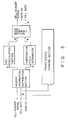
- Fig. 3 shows the arrangement of the CIS. The arrangement and schematic operation of the CIS will be described below with reference to Fig. 3.
- the CIS has a function of scrambling the information field of a cell transferred from the RTD via the OMDI, calculating an HEC in the header field, and writing the calculation result in an HEC field.
- the CIS receives a cell having a 53-byte length from the RTD in the format that a 1-bit header display signal is added to 18.72-MHz 8-bit parallel data.
- the CIS includes an HEC calculation section, and an information field scrambler. Header information of an input cell is selectively input to the HEC calculation section, and its information field is also selectively input to the information field scrambler. This selection is controlled by a counter which is reset in response to the header display signal parallel to a data line. Note that the information field scrambler is realized by a 43rd-order self synchronization type scrambler.
- Bit streams output from the HEC calculation section and the information field scrambler are mixed to reform a cell, and the cell is output.
- This output is 18.72-MHz 8-bit parallel data, and a header display signal of the cell is output parallel to the data.
- the header display signal is utilized when the FAS generates the H4 pointer of the VC-4.
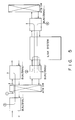
- the CSD is arranged as shown in Fig. 4.
- the CSD has a role of searching a cell header from the bit stream of the 18.72-MHz 8-bit parallel data transferred from the FDA by an HEC calculation, and putting a predetermined mark on the start byte of the searched cell.
- the 8-bit parallel data stream input from the FDA it is basically assumed that byte phases of cells are aligned.
- the CSD searches a cell header under the above-mentioned assumption for the sake of reducing consumption power, and outputs the cell in the form that a 1-bit header display signal is added to the 18.72-MHz 8-bit parallel data.
- the CSD is schematically operated as follows.
- a bit stream input from the FDA is input to a cell synchronization section.
- the cell synchronization section achieves cell synchronization with the input bit stream, and performs bit error detection/correction of a header field of a cell.
- the cell synchronization procedure, and the header field error detection/correction procedure in the cell synchronization section are executed as follows according to the CCITT.
- the cell synchronization section has three different states depending on a state of the cell synchronization procedure. Assume that a state wherein no cell synchronization is attained is referred to as a HUNT state, a state wherein cell synchronization is about to be attained is referred to as a PRESYNC state, and a state wherein cell synchronization is attained is referred to as a SYNCH state.
- HUNT state every time 1-byte data is input from the FDA, a syndrome of previously input 40 bits (5 bytes) is calculated.
- the previously input 40 bits are assumed to be a header, if the header includes no error, the calculated syndrome has a value which can be predicted beforehand. Therefore, when the syndrome has the predicted value, the FDA assumes that a header input is completed, and the state transits to the PRESYNC state.
- the FDA performs error detection of a header portion in units of cells. More specifically, the FDA calculates a syndrome of previously input 40 bits every time 53 bytes are input from when the HUNT state transits to the PRESYNC state. If the calculated syndrome has the above-mentioned predicted value for a successive DELTA number of times, it is determined that a portion presently assumed to be a header is surely the header, and the state transits to the SYNCH state. However, if the calculated syndrome does not have the predicted value, the state immediately returns to the HUNT state.
- the FDA performs error detection/correction of a header field in units of cells. In this process, since the position of a header field of a cell is correctly recognized, almost no error can occur. However, if an error is found in the header field for a successive ALPHA number of times, the state returns to the HUNT at that time.
- the CSD In the HUNT state and the PRESYNC state, the CSD does not output valid cells, but always outputs empty cells.
- the SYNCH state if no bit error is found in the header field, or if a bit error is found but is corrected, the corresponding cell is output to a dual buffer as a valid cell. An invalid cell is discarded. If there is no valid cell to be output to the OMDI, the CSD always outputs empty cells.
- An information field of a cell output from the cell synchronization section when the cell synchronization section is in the SYNCH state is descrambled by the information field descrambler.
- the descramble processing is executed by using a 43rd-order self synchronization type descrambler.
- a cell passing through the descrambler is temporarily stored in the dual buffer.
- An empty cell generator always generates empty cells to be output from the CSD.
- cells are stored on the dual buffer, one empty cell on the empty cell flow is replaced with a cell on the dual buffer, thereby outputting a valid cell.
- a cell synchronization operation is synchronized with a cell output operation.
- the 8-bit parallel data output from the CSD is added with the 1-bit header display signal.
- the cell header is displayed by a pointer H4 as described after
- 8-bit parallel data input to the CSD may be added with the header display signal.
- the CSD compares a cell header indicated by the header display signal, and a cell header calculated by itself by an HEC calculation, and if the two cell headers do not coincide with each other, the CSD generates an alarm to the ILC.
- the FDA detects a cell header based on the H4 pointer of the VC-4, adds the detected header field to 8-bit parallel data to be output, and transfers the data to the CSD, when error frame synchronization or error cell synchronization occurs, the cell header indicated by the header display signal is different from a cell header calculated by the HEC calculation. As a result, it can be informed to the ILC that one of the error frame synchronization and error cell synchronization has occurred.
- the comparison between the cell headers can be performed only when the header display signal is activated. Thus, when no header display signal is used, the signal is always fixed at inactive level to eliminate the influence on an operation of the CSD. If this signal is added to the CSD input interface, no problem is particularly posed.
- Observation information output from the CSD includes a state of the cell synchronization section, i.e., the HUNT, PRESYNC, or SYNCH state, an error frame/cell synchronization display signal if detection is performed, and a receiving off signal from the FDA.
- the receiving off signal from the FDA can be detected by observing data transferred from the FDA to the CSD, and supervising that all the data are fixed to be "0"s or "1"s for one cell time or more, since both logic values "0" and "1" always appear in a cell according to, e.g., a cell format determined by the CCITT.
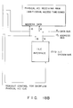
- the OAM cell insert/drop function is supported by the OMDI (Operation and Management Cell Drop and Insert) of the general arrangement of the cell processing function shown in Fig. 2.
- the OAM function (in particular, an ATM layer) is an issue under discussion in the CCITT, and may drastically change in future.
- the OAM function is realized as the following function to suppress a hardware scale as the primary object.
- the OAM function supported by the OMDI is realized, as shown in Fig. 5.
- the OMDI provides functions necessary for performing connection tests of a cell transfer path, and more particularly, provides functions for executing the following four tests.
- the adjacent node loop back test is a cell loop back test executed between adjacent nodes via a link system.
- the header format of the ATM layer OAM cell used for the above-mentioned ATM layer function tests is not standardized by the CCITT yet.
- the above-mentioned tests can be executed in such a manner that a VPI for identifying a VP link/connection to be tested is added based on the analogy between the header formats of an empty cell and a physical layer OAM cell, and a format having a PT field set with [10] is set.
- these tests are performed by setting a bit for designating, in the information field of the ATM layer OAM cell, whether at least the OAM cell is dropped or looped back, and a drop/loop back bit.
- a field indicating a test level of the cell i.e., a test level field is set in the information field of the physical/ATM layer OAM cell.
- the format of the OAM cell/OAM function must be matched with the link system. Therefore, of the physical/ATM layer OAM cells, an OAM cell having a test level field set with a specific pattern is assumed to be switched by a VPI in the link system in the same manner as normal cells. In addition, assume that a physical layer OAM cell which is designated with a loop back operation by the drop/loop back bit must be looped back on the link system.
- All the OMDIs in the node system have a function of dropping/looping back all the OAM cells according to their drop/loop back bits, and as a result, the above-mentioned four OAM functions can be realized.
- upstream/downstream VCs must be set using the same VPI/VCI. In this case, a loop back operation can be quickly performed. However, such setting need not always be made. If upstream/downstream VCs are set using different VPIs/VCIs, the OAM cell is temporarily transferred to the ILC, and after the VPI/VCI is rewritten by the ILC, the cell may be inserted in the opposite side, thereby realizing the loop back operation. Also, note that an OMDI of the link system used to be paired with this OMDI will be described later.
- This OMDI is arranged, as shown in, e.g., Figs. 6A and 6B.
- This OMDI has a function of swapping an active system and stand-by system in addition to the OAM cell insert/drop function.
- the two functions of the OMDI are realized on the basis of the fact that it is natural to execute the OAM cell insert/drop function and the active/stand-by swapping function using the same function elements since a swapping system checking operation must be performed by OAM cells when systems are swapped due to, e.g., instantaneous disconnection-free expansion.
- the OMDI is schematically operated as follows. OMDIs arranged in the respective sections of the system can be arranged by omitting unnecessary functions from this OMDI.
- OMDI inserted between CSD and RTA and OMDI inserted between RTD and CIS may be constructed in common with the structure show in Fig. 6.
- a cell input from an A system/B system input port is temporarily stored in a dual buffer to be synchronized with the operation cycle in the OMDI. This processing is performed so as not to cause cell discard upon selection of an A system/B system.
- the A system/B system means one of two systems to be swapped.
- task allotment of two systems such as the active system/stand-by system is not defined by this OMDI but by software. Therefore, in this case, a description will be made using simply the A system/B system.
- a cell passing through the dual buffer passes through a cell drop.
- the cell drop drops the cell when the following two conditions are established.
- one of the A and B systems of a cell flow passing through the cell drop is selected via a selector.
- the system-selected cell flow passes through a cell drop/empty cell exchanging section for realizing a loop back function.
- This cell drop drops the cell when the following two conditions are established.
- a cell flow passing through the cell drop then passes through an empty cell exchanging section.
- the empty cell can be exchanged with a cell to be inserted.
- the cell to be inserted is prestored in a buffer connected to the empty cell exchanging section.
- the empty cell exchanging function corresponds to a loop back cell insert function.
- a cell flow passing through the empty cell exchanging section is copied to the A system/B system, and then passes through a gate.
- This gate determines whether or not the received cell is output to the A system/B system. If it is determined that the received cell is not output, an empty cell flow is output to the A system/B system.
- the gate has an empty cell generating function.
- a cell flow is copied to provide the same cell flow, so that substantially the same internal states of ATMSWs can be maintained in the A system/B system to prepare for swapping between systems upon occurrence of a trouble.
- the reason why the cell flow temporarily passes through the gate to select whether or not the cell flow is output to the A system/B system after it is copied is as follows. That is, selection is made so that a checking operation of a system which is not presently used as that for an instantaneous disconnection-free system swapping operation does not adversely influence a switched traffic.
- the empty cell exchanging function realizes an insert operation of an OAM cell, and is realized as a function allowing to independently insert OAM cells in the A system/B system so as to swap between systems to be free from an instantaneous disconnection.
- an empty cell is detected from a given cell flow, and a header cell in a cell string stored in a buffer is exchanged with the detected empty cell, thereby realizing the empty cell exchanging function.
- an OAM cell insert function can be realized.
- the loop back cell drop In order to conduct the loop back test, the loop back cell drop must have a function of changing the drop/loop back bit of an OAM cell from a loop back mode to a drop mode.
- an OAM cell cannot pass through a path between the A system/B system cell drop to the A system/B system empty cell exchanging section. Therefore, in this case, as shown in Fig. 6, a special OAM cell, more specifically, an OMDI-OAM cell may be flowed between these sections to check the operation of the path.
- a special OAM cell more specifically, an OMDI-OAM cell may be flowed between these sections to check the operation of the path.
- another function element detects a receiving off signal, and as will be described later, since the TOVA counts the number of passing cells in units of VPs, a checking operation of the path using the OAM cell is not necessary in practice.
- the observation information output from this OMDI consists of drop cell discard information and insert cell discard information in the empty cell exchanging sections arranged at a total of three portions, and their buffers, i.e., the cell insertion functions.
- the controller detects that an OAM cell to be inserted is discarded, and changes an OAM procedure so as not to cause a contradiction.
- Fig. 7 illustrates an OAM cell interface method between the OMDI and the ILC.
- the OMDI has a total of four ports for inputting/outputting an OAM cell to/from the ILC.
- a DMA transfer operation is performed between these ports and an MM (main memory) of the ILC, thereby interfacing between the ILC and the OMDI.
- the ILC must recognize a port from which an OAM cell is dropped, or a port to which an OAM cell is to be inserted. Therefore, as shown in Fig. 7, DMA channels are provided to the respective OAM cell input/output ports of the OMDI, and the ILC identifies the DMA channel, thereby identifying a port to/from which an OAM cell is input/output.
- the VPI transformation & routing tag addition function in the above-mentioned cell processing function will be described below.
- the VPI transformation & routing tag addition function is supported by the RTA (Routing Tag Adder), the LPT (Logical/Physical VCI Transformer), and the HTT (Header Transformation Table).
- 128K VCs are simultaneously set on a 155-Mbps link, an average speed per VC is 146 bps, and the B-ISDN is rarely used in this manner.
- a system In order to realize header transformation functions/polishing functions for 128K VCs, a system inevitably has a scale which cannot be allowed by the existing LSI technologics. Therefore, the number of simultaneously connected lines is calculated in the following manner.
- the number of simultaneously connected lines is set to be a maximum of 4,096 in consideration of the presence of VCs having speeds lower than the 64-Kbps channels.
- mapping from a 128K (logical) VC space formed by VPIs/VCIs to a 4K (physical) VC space to be actually processed must be performed, and identifiers must be set for the respective mapping operations.
- VPI+VCI input to a node system while being carried by a cell is referred to as a logical VCI
- an identifier for identifying simultaneously connected VCs is referred to as a physical VCI
- the LPT serves as a function element for performing identifier transformation from the logical VCI to the physical VCI.
- a transformation algorithm from the logical VCI to the physical VCI in the LPT is expressed as shown in, e.g., Fig. 8.
- lower 3 bits of a VPI and lower 3 bits of a VCI in the logical VCI are used as lower 6 bits out of 12 bits of the physical VCI.
- Other bit positions of the logical VCI may be used as 6 bits of the physical VCI, they do not influence the effectiveness of the present invention.
- An associative memory is accessed using the remaining 22 bits of the logical VCI as a key, thereby obtaining the remaining 6 bits of the physical VCI.
- each CAM word compares a 22-bit associative key stored therein with 22 bits transferred from the logical VCI register. If its own associative key coincides with the transferred 22 bits, the CAM word externally outputs 6-bit associative data stored therein. If a noncoincidence is found, the CAM word outputs no data.
- the 6-bit associative data output in this manner is sent to the physical VCI register, thus obtaining the physical VCI at that time.
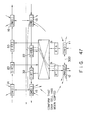
- the RTA has an arrangement, as shown in Figs. 10A and 10B.
- the 3P-RAM is a 3-port RAM having one write port and two read ports, and has a storage capacity of 64 words (32 bits/word). These read/write ports can be asynchronously operated.
- the storage area of the 3P-RAM is divided into four blocks each having one cell length, and block #.
- An operation between a cell input to the write port of the 3P-RAM is performed in synchronism with data CK1, and other operations are performed in synchronism with data CK2.
- a cell input in synchronism with external data CK1 (18.72 MHz) is converted to have a 32-bit width by SP (serial/parallel conversion).
- the 32-bit data is written in the 3P-RAM from its write port (WP) via two 32-bit registers.
- WP write port
- a write block of the 3P-RAM is selected from an empty block list of a W address formation section, and write access is made in synchronism with the data CK1.
- the R address formation section which received the block # of the cell write-in completion block reads out a VPI/VCI of a cell stored in the block having the corresponding number (i.e., one work including it) using the read port 1 (RP1) of the 3P-RAM, and informs the VPI/VCI to the LPT as the logical VCI.
- the LPT transforms the informed logical VCI into the physical VCI.
- the LPT informs the physical VCI to the HTT.
- the HTT makes a table access using the physical VCI, and informs, to the RTA, the following five pieces of information (1) to (5), which are exchanged when the corresponding cell is output.
- the R address generating function of the RTA is realized in such a manner that read access of a cell stored in a block having the next block # from the read port 2 (RP2) is started, and the five pieces of information informed from the HTT as described above are merged with data which is being read out from the RP2 using a selector, thereby format-converting data into a cell having a format which can be transferred to the following function elements.
- a VPI rewrite position is changed in accordance with UNI/NNI informed from the HTT. More specifically, when the NNI is designated, 12 bits are rewritten as a VPI, and when the UNI is designated, 8 bits excluding a GFC field are rewritten. With this processing, a case wherein a UNI/NNI cell flow passes one RTA is coped with.
- the block # of the block which stores the corresponding cell is transferred to the W address formation section as a cell readout completion block #. Thereafter, a parity addition section adds a parity bit to a cell which is format-converted as described above, and the cell is output.
- the R address formation section transfers the block # of an empty block to the W address formation section in a handshake manner upon completion of the cell output operation.
- the VPI/VCI read operation from the RP1 and cell read/output operation from the RP2 are executed in a pipeline manner.
- an alarm cell is formed based on routing tags registered in all the entries of the HTT and a new VPI/VCI upon an instruction from the ILC, and is externally output. The necessity of this function will be described in detail later.
- a cell standardized as a UNI/NNI will be referred to as a UNI/NNI cell hereinafter, and a cell obtained by adding additional information to the UNI/NNI cell to enable switching by the ATMSW will be referred to as an SW cell hereinafter.
- Fig. 11 shows formats of the UNI/NNI cell and the SW cell.
- the SW cell is formed by adding a total of 11 bytes of additional information to the UNI/NNI cell, the SW cell being a cell having a format capable of switching by the ATMSW.
- the additional information includes:
- an alarm cell is formed by, e.g., the ILC and is output through the OMDI to two end points of a VC connection passing through a cell processing function in trouble, a considerable time is inevitably required.
- a maximum of 4,096 VC connections pass through each cell processing function, even if the ILC can output an alarm cell at 256 Kbps, a maximum of about 8 seconds are required until the ILC outputs the alarm cell to one end point of each of all the VC connections. Therefore, an alarm cell must be automatically generated somewhere.
- an alarm cell automatic generating function can be assembled in the RTA.
- An alarm cell must be generated toward not only a VC connection terminal end point for outputting a cell but also a VC connection terminal end point for receiving a cell.
- an alarm cell generated toward the VC connection terminal end point for outputting a cell is input to the VC connection at a trouble-free point closest to a trouble point in the VC connection, it can be automatically transferred to the VC connection terminal end point for outputting a cell.
- a VC connection does not have a cell transfer function toward its connection terminal end point for receiving a cell. Therefore, an alarm cell must be transferred via the same cell processing function as the VC connection in trouble using a VC connection having an opposite cell flow direction. For this reason, when VC connections are set, VC connections for transferring cells in the opposite direction must be set. In this case, even if VC connections having only one direction are to be set, those having the opposite flow direction must be set.
- the alarm cell automatic generating function generates an alarm cell while setting the following three trouble levels.
- Level 1 This level is set when a trouble such as an STM frame synchronization error or a cell synchronization error in the former stage (FDA, CSD, OMDI) in the RTA is detected.
- Level 2 This level is set when a trouble of the entire cell processing function, e.g., runaway of the ILC, disconnection of a power supply of the cell processing function, a receiving off state in the RTD, or the like occurs.
- Level 3 This level expresses a trouble of the entire node, e.g., runaway of the supervision controller, disconnection of an intra-node communication optical link, or the like.
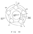
- Fig. 13 is a view showing the relationship between troubles at the above-mentioned levels, and portions for automatically generating alarm cells according to the trouble levels.
- alarm cell generating portions toward VC connection terminal end points for outputting a cell vary depending on the trouble levels. More specifically, when a trouble at level 1 occurs, the RTA whose former stage malfunctions generates an alarm cell. When a trouble at level 2 occurs, an RTD in a cell processing function which receives a cell from the cell processing function in trouble via the ATMSW generates an alarm cell. When a trouble at level 3 occurs, an RTA in a cell processing function opposing a node system in trouble generates an alarm cell.
- alarm cells toward VC connection terminal end points for receiving a cell are generated by an RTA in a cell processing function opposing the cell processing function in trouble via a communication path.
- This RTA generates alarm cells as follows. More specifically, the RTA sequentially generates alarm cells having new VPIs/VCIs set in the HTT in their header field. Such generation of the alarm cells can be realized by sequentially reading out new VPIs/new VCIs, and routing tags from the HTT, and causing the RTA to form SW cells using these data.
- the RTD generates alarm cells as follows. More specifically, module number, which is information indicating cell processing function from which cell flow is to be received, is stored in units of new VPI/new VCI. When a trouble occurs in a given cell processing function, the corresponding module number is informed to all the trouble-free cell processing functions. Each trouble-free cell processing function detects a VC connection to which alarm cells must flow on the basis of the informed module number, and flows alarm cells through the VC connection.
- This processing can be realized in such a manner that a table from which a cell processing function number can be searched based on new VPI/new VCI numbers is sequentially searched, and if the informed module number is written in the table, an alarm cell having a VPI/VCI number obtained from the table in its header portion is formed and output.
- the VPI/VCI as the logical VCI is transformed into the physical VCI, and table look-up of the HTT is performed using the VCI, as described above. Therefore, the alarm cell generating function in the RTD also requires a transformation function from the logical VCI to the physical VCI.
- a shaping channel number for VP shaping or VC shaping in the SW cell since leaky buckets are prepared in correspondence with the number of simultaneously connected lines, they can be regarded as a kind of physical VCIs at the output port of the ATMSW. Therefore, when an alarm cell generation table is arranged to output a new VCI, a new VPI, and a module number on the basis of the shaping channel number, the above-mentioned alarm cell generating algorithm can be directly used.
- an alarm cell can be distinguished from other cells using, e.g., a PT field, or by using a VPI unique to the alarm cell.
- a bit for designating this can be set in an information field or a PT field of the cell.
- the above-mentioned HTT is arranged and operated as follows.
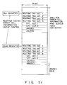
- Fig. 14 shows an address map of the additional information table.
- This additional information table is realized as a structure having an entry of 128-bit length for each of 4K physical VCIs, and the entry is divided into the following fields.
- Parity bits are assigned to the respective words of the additional information table having the above-mentioned architecture. These parity bits are even parity bits, are set by the ILC, and are checked when the corresponding words are read out from the static RAM array.
- Fig. 15 shows a schematic arrangement of the HTT having the above-mentioned additional information table.
- the HTT comprises the above-mentioned additional information table, and two access ports allowing accesses to the additional information table from the RTA and the ILC.
- the access port for the RTA receives a physical VCI from the LPT, and a 3-bit address for designating a word in an entry from the RTA.
- the HTT reads out one word from the RAM array using the input information as an address, and supplies the readout word to the RTA.
- the HTT calculates an even parity of the word, and checks a coincidence with the parity bit.
- the HTT checks an entry effective flag in the entry corresponding to the physical VCI supplied from the RTA. In this case, if the entry effective flag is not set, the HTT determines an improper physical VCI, and informs this to the RTA.
- the HTT supplies the physical VCI at that time to the ILC. At this time, the rewrite position of the RTA is designated according to the content of the UNI/NNI designation flag.
- the access port for the ILC serves to make the RAM array look like the memory area of the ILC.
- the ILC executes read/write access of words using addresses assigned in units of words.
- An access request from the ILC and an access request from the RTA must be arbitrated therebetween, so that HTT readout signal of RTA and ILC access signal are used.
- the cell flow observation/cell discard control/polishing function is realized as a function supported by the TOVA (Traffic Observation/Violation Tag Adder) and the IBUF (Input Buffer) of the general arrangement of the above-mentioned cell processing function.
- the IBUF executes speed conversion of a cell flow in addition to the cell flow observation/cell discard control/polishing function.
- the mounting position of the polishing function corresponds to an input-side terminal end point of a VC connection. More specifically, the polishing function is assembled in a subscriber's side input point of the cell processing function accommodating a T B point such as an input side from the transmission path of the BUNI.
- the cell flow observation/cell discard control/ polishing function can provide the following functions.
- the LPT supplies a physical VCI to the TOVA simultaneously with the HTT.
- the TOVA observes a cell flow in accordance with the supplied physical VCI, and detects a passing traffic amount in units of VCs. When the passing traffic amount exceeds a preset value, this is informed to the RTA, and the corresponding cell is determined as a violation cell. Thus, [1] is set in a violation tag field of an SW cell.
- a cell which is designated as a physical layer/ATM layer OAM cell by a PT field also serves as an object in traffic observation.
- the IBUF executes cell discard control according to a predetermined algorithm. Cells are discarded in only the IBUF.
- the cell discard control handles cells to be discarded when a new cell is input in an IBUF full state. Note that when a cell determined as a violation cell by the TOVA is discarded, the cell discard control serves as polishing control.
- a problem of which of a cell determined as a violation cell by the TOVA, and a cell which is defined as a cell to be easily discarded by the CLP is preferentially discarded, is posed.
- a cell which is designated as a physical layer/ATM layer OAM cell by a PT field must be avoided from being discarded if possible.
- the cell flow observation 5 function is supported by the TOVA, and the TOVA not only counts the number of passing cells in units of VCs as a network management parameter, but also observes the following polishing parameters. More specifically, traffic characteristics determined by VCs include a peak rate and an average rate. The detailed parameters of the traffic characteristics determined by the VCs are defined as follows, and these parameters can be set in units of VCs.
- peak rate peak rate observation leaky bucket counters arranged in units of VCs are incremented upon arrival of cells, and are decremented at the T0 period. When the value of the counter is 0 upon decrementing of the counter, no further decrement operation is performed. A cell arrived when the value of the counter exceeds Th is determined as a violation cell, and its peak rate is observed.
- average rate observation leaky bucket counters arranged in units of VCs are incremented upon arrival of cells, and are decremented at a [T1/N1] period. However, when the value of the counter is 0, no further decrement operation is performed. When cells arrive with no violation against the traffic characteristics, the value of the counter may be maximized, for example, when N1 cells continuously arrive at a peak rate. In this case, the value of the counter becomes a maximum of: N1(1-TON1/T1).
- the arrived cell is detected as a violation cell, and an average rate is observed based on this cell.
- the RTA which is informed that a presently passing cell is a violation cell, sets a violation tag field of the cell to be [1].
- the above-mentioned cell flow observation algorithm is realized as a basic arrangement of leaky buckets used in observation of polishing parameters in the TOVA, as shown in, e.g., Figs. 16A and 16B.
- This algorithm requires peak rate observation leaky buckets and average rate observation leaky buckets in units of VCs, and is realized by constituting these leaky buckets using the following four types of registers.
- registers are respectively arranged as registers (LBCP, LBTHP, DPCP, DPTHP) for observing a peak rate, and those (LBCA, LBTHA, DPCA, DPTHA) for observing an average rate.
- a period, determined based on the minimum cell arrival time interval T0, for decrementing the LBCP is set in the DPTHP for every cell period.
- the DPCP is incremented for every cell period, and is cleared when its value reaches a value set in the DPTHP. Every time the DPCP is cleared, the LBCP is decremented.
- the LBCP is incremented every time a cell arrives.
- the LBTHP is set with a threshold value for determining a violation cell determined by the above control strategy.
- the value of the LBCP is compared with a value held in the LBTHP.
- a cell which is being input is determined as a violation cell.
- the LBCP is no longer incremented.
- the DPTHA is set with a period, determined based on a predetermined value [T1/N1 T0], for decrementing the LBCA for every cell period.
- the DPCA is a counter incremented for every cell period, and is cleared when its value reaches a value set in the DPTHA. Every time the DPCA is cleared, the LBCA is decremented.
- the LBCA is incremented every time a cell arrives.
- the LBTHA is set with a threshold value for determining a violation cell determined by the control strategy like in the LBTHP.
- the value of the LBCA is compared with a value held in the LBTHA.
- a cell which is being input is determined as a violation cell.
- the LBCA is no longer incremented.
- the lengths of these registers used in observation of the UNI/NNI are basically determined based on the periods which define the peak rate and the average rate.
- the peak rate is defined as a period of about 100 mSec
- the average rate is defined as a period of about 1 Sec
- the length of each peak rate observation register is determined to be 16 bits
- the length of each average rate observation register is defined to be 20 bits.
- 144-bit flip-flops are required in units of VCs.
- since the maximum number of simultaneously connected lines per link is 4,096, about 590-Kbit information per link is required to observe the polishing parameters.
- the number of effective gates in a gate array which can be presently utilized is about 50K gates. Therefore, in order to realize the cell flow observation function by a proper number of LSIs (several LSIs or less per link), an improvement in the degree of integration of the LSIs by one hundred times or more from the present level must be waited when the above-mentioned arrangement is employed.
- the DPCP and DPCA as the counters for generating the decrement periods of the LBCP and LBCA must be incremented for every cell period.
- the cell period is a time period necessary for transferring one cell, and more specifically, is about 2.7 ⁇ sec. Therefore, even if the DPCP and DPCA are allocated on different RAMs, a total of 8,096 read and write accesses must be generated to these RAMs in only decrement operations of the DPCs.
- a VC which must control the decrement operations of the LBCP and LBCA for every cell period has a relatively short minimum cell arrival time interval T0, i.e., has a relatively high peak rate.
- the VC can be considered as a VP having a minimum cell arrival time T0 of up to several hundreds of ⁇ Sec, i.e., a peak rate of several Mbits.
- ⁇ Sec i.e., a peak rate of several Mbits.
- a polishing parameter observation section of the TOVA in a single physical interface is arranged on the basis of the following viewpoints, and an LSI having an existing degree of integration/speed is realized using a proper number of chips.
- a peak rate observation register for holding the number of decrement operations executed during the 1,024-cell period is called a VPD (Decrement Value, Peak), and an average rate observation register is called a DVA (Decrement Value, Average).
- the lengths of these registers are 7 bits. In this case, the lengths of the DPCP and the DPTHP can be shortened to 6 bits, and the lengths of the DPCA and DPTHA can be shortened to 10 bits.
- the low-speed channel leaky buckets when the low-speed channel leaky buckets for observing the VCs determine a violation cell, or when the high-speed channel leaky bucket for systematically observing these leaky buckets determines a violation cell, it is determined that a cell which is being input is a violation cell.
- the LBCA and the LBCP When the LBCA and the LBCP are decremented at the 1,024-cell period, cells may arrive at offset timings beyond the given traffic characteristics.
- the number of minimum cell arrival time intervals T0 of VCs to be observed by the low-speed channel leaky buckets is at most 32 (normally, it is still larger than 32), and the high-speed channel leaky bucket independently observes all the VCs to be observed by the low-speed channel leaky buckets, resulting in no influence in practical applications.
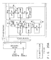
- Figs. 17A and 17B show the schematic arrangement of the TOVA.
- the TOVA shown in Figs. 17A and 17B is realized to comprise a function of counting the number of passing cells in units of VCs in addition to the polishing parameter observation function.
- a physical VCI supplied from the LPT is input to a physical VCI reception function.
- the physical VCI reception function obtains a number of a leaky bucket for observing the corresponding VC in accordance with information written in a RAM connected to the function element, and information written in a physical VCI reception RAM.
- the value of a counter which holds the number of cells passing through the corresponding VC is read out from the physical VCI reception RAM, is incremented, and is written in the counter.
- the received physical VCI is enqueued in an overflow physical VCI queue allocated in the physical VCI reception RAM in order to inform the overflow state to the ILC.
- Leaky buckets respectively have leaky bucket numbers.
- leaky bucket numbers [0] to [30] are assigned to high-speed channel leaky buckets
- leaky bucket numbers [31] to [4,095] are assigned to low-channel leaky buckets.
- a leaky bucket number [31] is assigned to a leaky bucket for systematically observing all the VCs to be observed by the low-speed leaky buckets.
- the physical VCI reception function causes the high- or low-speed leaky bucket to increment its LBCP or LBCA according to the leaky bucket number as a result of table lookup. As a result of the increment operation, if a cell being output from the RTA is determined as a violation cell, a message indicating this is displayed on the RTA using a violation cell signal.
- the high-speed channel leaky bucket is constituted by adding an ILC interface for performing accesses from the ILC to respective registers, and a decoder for selecting one of the 32 leaky buckets according to a leaky bucket number received from the physical VCI reception function to an arrangement obtained by simply connecting 32 circuit arrangements shown in Fig. 16.
- the low-speed channel leaky bucket is constituted by a leaky bucket RAM for holding information necessary for a leaky bucket operation, and a low-speed channel leaky bucket controller as a controller for realizing the leaky bucket operation on the RAM.
- the physical VCI reception RAM and the leaky bucket RAM are realized to be seen from the ILC as if they were storage areas assigned to a memory area. For this reason, one of an access from the ILC interface, and an access from the physical VCI reception function or the low-speed channel leaky bucket controller is selected by a selector, and the selected access is supplied to these RAMs. When accesses from two directions collide or contend with each other, arbitration is made to cause, e.g., an access from the ILC side to wait.
- Figs. 18A and 18B show an arrangement of the above-mentioned physical VCI reception function.
- the physical VCI reception function executes four different operations, i.e., (1) an operation for obtaining a leaky bucket number for observing the corresponding VC from a physical VCI, (2) an increment operation of counters for counting the numbers of passing cells in units of VCs, (3) an operation for, when the passing cell counter overflows, enqueuing a physical VCI corresponding to the overflowing counter to an overflow physical VCI queue, and (4) an operation for arbitrating accesses from the ILC to the physical VCI reception RAM.
- four different operations i.e., (1) an operation for obtaining a leaky bucket number for observing the corresponding VC from a physical VCI, (2) an increment operation of counters for counting the numbers of passing cells in units of VCs, (3) an operation for, when the passing cell counter overflows, enqueuing a physical VCI corresponding to the overflowing counter to an overflow physical VCI queue, and (4) an operation for arbitrating accesses from the ILC to the physical VCI reception RAM.
- the operation for obtaining the leaky bucket number for observing the corresponding VC from the physical VCI is executed as follows.
- a physical VCI input from the RTA is input to a physical VCI register.
- the physical VCI held in the physical VCI register is held until a series of processing operations for the physical VCI are completed.
- [physical VCI leaky bucket number transformation] control is enabled.
- the [physical VCI leaky bucket number transformation] control is executed by accessing a [physical VCI leaky bucket number transformation table] of the above-mentioned VCI reception RAM using the value held in the physical VCI register as an offset, thereby obtaining a leaky bucket number corresponding to the physical VCI.
- the leaky bucket number obtained from this table is held in a leaky bucket #; register. Based on information held in the leaky bucket #; register, a high- or low-speed channel leaky bucket is selected, and the corresponding leaky bucket number is incremented.
- the passing cell counters are then incremented. With this passing cell count control, processing for making a read access to a passing cell counter area in the physical VCI reception RAM using the value held in the physical VCI register as an offset, incrementing the readout data, and writing the incremented data at the same address is executed.
- overflow physical VCI queue control when the readout data is incremented, if the data overflows, overflow physical VCI queue control is enabled.
- the received physical VCI is enqueued in an overflow physical VCI queue allocated in the physical VCI reception RAM.
- a ring buffer is formed in the physical VCI reception RAM.
- a header pointer and a tail pointer are arranged.
- the above-mentioned operation is continuously performed when a physical VCI is input from the LPT.
- an access from the ILC to the physical VCI reception RAM is performed when the above-mentioned operation is not performed.
- contention control of accesses to the physical VCI reception RAM is performed. Note that accesses from the ILC to the physical VCI reception RAM include the following three patterns:
- the accesses (1) and (2) are normal accesses for the memory.
- the access (3) is an access for dequeuing information from the ring buffer. This dequeuing is performed with the assistance of the overflow physical VCI queue control.
- Figs. 19A and 19B show an address map of the above-mentioned physical VCI reception RAM.
- a physical VCI leaky bucket # transformation table area a passing cell counter area, and an overflow physical VCI queue ring buffer area are assigned in turn from lower addresses.
- An entry for each physical VCI in the physical VCI leaky bucket # transformation table has a 2-byte length. Of 2 bytes, 12 bits are assigned to a leaky bucket number.
- An Inc enable bit is bit information for, when a physical VCI corresponding to an entry of this bit is input, designating whether or not an increment operation of the leaky bucket is to be performed. This bit is checked before the beginning of use of the leaky bucket.
- this entry includes a high-speed polishing/low-speed polishing bit for designating a high- or low-speed leaky bucket for observing a VC corresponding to the entry for the purpose of reducing the number of hardware components. The remaining 2 bits are unused.
- an entry corresponding to each physical VCI in the passing cell counter area has a 4-byte length. Of 4 bytes, 3 bytes constitute the passing cell counter. Since this counter is a 24-bit counter, it overflows once per about 30 seconds at 150 Mbps and 100% load. Note that the remaining 8 bits are unused.
- the overflow physical VCI queue ring buffer area is designated by the head or tail pointer to have 2 bytes as one word. Of 2 bytes (one word), the above-mentioned physical VCI is stored using 12 bits. Note that the remaining 4 bits are unused.
- Figs. 20A and 20B show a schematic arrangement of the high-speed channel leaky bucket.
- the high-speed channel leaky bucket is constituted by the 32 polishing leaky buckets shown in Fig. 16 described above, a decoder for supplying an increment request to one of these leaky buckets in accordance with an input leaky bucket number, and an ILC interface for allowing read and write accesses of LBCP, LBCA, LBTHP, LBTHA, DPTHP, and DPTHA from the ILC to registers.
- flags called DDA and DDP are used for designating whether or not a decrement operation is performed in the leaky bucket. These flags can be set/reset under the control of the ILC, and are checked before the beginning of use of the leaky bucket.
- Figs. 21A and 21B show a schematic arrangement of the low-speed channel leaky bucket controller.
- the low-speed channel leaky bucket controller comprises a register array for temporarily storing data to be supplied to an ALU, the ALU for executing arithmetic operations for realizing the leaky buckets, and transfer and arithmetic control sections for controlling information transfer among these components.
- This ALU is realized by using, e.g., a 32-bit ALU of a mega cell function library for a CMOS gate array. Since the register array stores predetermined information, the number of hardware components necessary for the register array can be decreased accordingly.
- Information transfer between the leaky bucket RAM and the register array, and information transfer between the ALU and the register array are performed through independent buses, so that pipeline processing for the ALU can be easily realized. With this arrangement, the throughput of the ALU, and the throughput of the leaky bucket RAM can be prevented from being decreased, and 4,096-channel polishing parameters can be observed.
- Information transfer between the leaky bucket RAM and the register array is controlled by the transfer control section, and control of the ALU and information transfer between the ALU and the register array are controlled by the arithmetic control section.
- These transfer and arithmetic control sections are realized as kinds of microsequencers. Micro codes of these sequencers are described in horizontal instructions (about 64 bits per word).
- a [0] clear AND gate array is added as a bus for transferring arithmetic results from the ALU to the register array.
- An access from the ILC to the leaky bucket RAM is made in the intervals of information transfer operations between the leaky bucket RAM and the register array. Since it is assumed that the ILC does not directly access the register array, and the micro codes of the microsequencers are supplied from a ROM, a load operation from the ILC is particularly not taken into consideration.
- the address map of the leaky bucket RAM is to store information necessary for performing the leaky bucket operation in a 16 bit x 8 word RAM, as shown in Fig. 22. The above-mentioned transfer operation is performed according to this address map.
- Fig. 23 shows an operation example of the above-mentioned transfer and arithmetic control sections.
- Fig. 23 when the above-mentioned registers for holding DPCP, DPCA, DPTHP, DPTHA, DVP, and DVA are duplexed, as shown in, e.g., Figs. 21A and 21B, a blank time can be prevented from being formed in the ALU operation, and the ALU can be sufficiently efficiently used.
- This operation example demonstrates that only one ALU can sufficiently function in the low-speed channel leaky bucket controller.
- the next arithmetic operation to be executed by the ALU must be changed in response to a carry output from the ALU.
- the arithmetic control section can determine on the basis of DDP (LBCP decrement ON/OFF designation) bit and the DDA (LBCA decrement ON/OFF designation) bit in the leaky bucket RAM whether or not the decrement operations of the LBCP and LBCA are performed. This function is used in a checking operation before the beginning of use of the leaky buckets.
- DDP LBCP decrement ON/OFF designation
- DDA LBCA decrement ON/OFF designation
- Observation information in this TOVA includes the following pieces of information.
- pieces of observation information of the TOVA for the physical VCI reception RAM, the high-speed channel leaky bucket, and the leaky bucket RAM are prepared as follows.
- mapping information from a physical VCI to a leaky bucket #, increment suppression information for each leaky bucket, high-speed channel leaky bucket/low-speed channel leaky bucket selection information, the passing cell counters in units of VCs, and passing cell counter overflow information in units of VCs are prepared.
- the passing cell counter for each VC overflows this is informed to the ILC by interrupt.
- various polishing parameters, a leaky bucket counter value, and leaky bucket decrement suppression information are prepared. Furthermore, for the leaky bucket #, various polishing parameters, a leaky bucket counter value, and leaky bucket decrement suppression information are prepared.
- the leaky bucket is inspected using the observation information as follows upon setting of a VC.
- a leaky bucket used in the VC suppresses a decrement operation, and causes an ATM layer OAM cell of the corresponding VC to pass through a plurality of RTAs. After the OAM cell passes, the leaky bucket confirms that the LBCA and LBCP are incremented in correspondence with the number of passed RTAs.
- the leaky bucket used in the VC suppresses an increment operation, and sets a proper value in the LBCA and LBCP. Thereafter, the leaky bucket starts the decrement operation as described above, and loads values of these counters at a timing at which the value becomes [0] when the counters are decremented at a preset decrement period. The leaky bucket confirms that the value becomes [0], thereby observing a cell.
- the cell discard control/polishing function will be explained hereinafter.
- the cell discard control/polishing function is supported by the IBUF.
- the IBUF has three functions, i.e., a function of inputting and storing SW cells, a function of outputting SW cells, and a function of discarding SW cells.
- a function of inputting and storing SW cells i.e., a function of inputting and storing SW cells
- a function of outputting SW cells i.e., a function of discarding SW cells.
- a mounting method of a buffer of this type may pose an important technical subject.
- FIFO function constituting a buffer such as the IBUF
- methods of realizing the FIFO function constituting a buffer such as the IBUF can be roughly classified into two types, and such classification is made on the basis of methods of holding a cell arrival order.
- the FIFO function can be realized by:
- the method (1) can be further classified into the following two types according to the way of utilizing the linear address space:
- the above-mentioned ring buffer method and the linked list method can use RAMs according to their realization algorithms. Therefore, when FIFO functions having the same capacity are to be constituted, these methods can be advantageously employed as compared to the above-mentioned shift register method. Which of these methods is to be employed is determined depending on additional functions other than the FIFO function. If a buffer of only the FIFO function is realized, the above-mentioned ring buffer method is more advantageous than the linked list method since it does not require an extra pointer area. However, when a buffer having a function of sharing one storage area among a plurality of processes to effectively utilize the storage area in addition to the FIFO function is realized, the linked list method is more advantageous.
- a shared buffer ATM switch As an example of a buffer for sharing one storage area among a plurality of processes to effectively utilize the storage area in the ATM system, a shared buffer ATM switch is known.
- processes correspond to cell buffering operations units of output routes. Therefore, the shared buffer ATM switch can be advantageously realized by the linked list method.
- cell discard control is performed.
- To execute the cell discard control in the IBUF means that the arrival order of cells is ignored, and cells are selectively discarded according to discard classes.
- selective discard of cells is constituted by two operations, i.e., a selection/discard operation of a cell to be discarded, and a reconstruction operation of the arrival order after the discard operation.
- discard class division is performed based on an OAM cell/CLP.
- the discard class division means that cells belonging to a VC have different discard classes. Therefore, a method of arranging independent buffers in units of classes cannot be directly used since a cell order may be reversed.
- the FIFO function is realized using the shift register method, since cells are spatially developed on D-FFs, cell discard regardless of the cell arrival order can be easily realized as compared to the above-mentioned linked list method and the ring buffer method.
- the FIFO function based on the shift register method can easily extract low-level parallel characteristics of the selection/discard operation of cells to be discarded, and the reconstruction operation of the arrival order after the cell discard operation, by utilizing the fact that, for example, cells are spatially developed on D-FFs. Therefore, when this method is utilized, the cell input/output and discard operations once per about 2 ⁇ sec can be easily realized by the existing LSI techniques.
- the above examination is the major reason for independently arranging a buffer (IBUF) for supporting discard classes in a proposed architecture, a buffer (ATM switch) for absorbing conflicts upon cell switching, and a buffer (OBUF) for supporting delay classes/smoothing.
- IBUF IBUF
- ATM switch ATM switch
- OBUF buffer
- Fig. 24 shows an arrangement of the IBUF.
- cells input from an input port are temporarily input to a dual buffer, and are synchronized with an internal operation cycle of the IBUF.
- the cells are input from the input port at a timing of 18.27 x (63/53) MHz in an 8-bit parallel format.
- bit information necessary for determining a discard class of the corresponding cell i.e., a violation bit, a PT field, and a CLP field are supplied to a discard control section.
- the discard control section detects the discard class of the cell using these pieces of information.
- a cell set with the violation bit is immediately discarded when it is output from the dual buffer.
- the cell to be discarded is stored in a FIFO connected to an ILC interface. If this FIFO is not empty, the ILC is interrupted at the corresponding level.
- the ILC fetches a discard cell via the ILC Interface when it is interrupted. At this time, a reception time of the discard cell is recorded based on an internal clock of the ILC, if necessary.
- the ILC may refer to a VPI/VCI of the cell, and may count the number of discarded cells for each VC. Assuming almost no cells are discarded in the ATMSW, the discard cell buffer need only have a length corresponding to one or two cells.
- a cell set with no violation bit is temporarily written in a 3P-RAM. If the 3P-RAM is not empty, one cell is selected from the 3P-RAM, and is discarded. The discarded cell is similarly held in the FIFO of the ILC interface, and waits until it is fetched by the ILC.
- the address space of the 3P-RAM is divided into blocks each of which can store one cell.
- An empty block # FIFO is a FIFO for storing a number of a block which does not store a cell in the 3P-RAM. When this FIFO is not empty, the IBUF is not full.
- the discard control section When a cell is input, the discard control section causes the empty block # FIFO to dequeue one block #.
- the dequeued block # is supplied to an input control section, and is enqueued in the block # FIFO together with the discard class of the cell which is being input.
- the empty block # FIFO When the empty block # FIFO is empty, the IBUF is full.
- the discard control section informs the block # FIFO to discard one block # while presenting the discard class of the cell presently being input.
- the block # FIFO selects a block which stores a cell whose discard class is equal to or smaller than the simultaneously informed discard class, and discards the block #.
- the block # discarded from the block # FIFO in this manner is informed to the discard control section first.
- the discard control section reads out the cell stored in the block having the informed block #, and transfers it to the buffer of the ILC interface. Thereafter, the block # of the empty block is informed to the input control section.
- the input control section When the block # is informed, the input control section generates a write address of the cell which is being input, supplies it to the 3P-RAM, and controls the write operation of the 3P-RAM. At the same time, the block # for receiving the cell is enqueued in the block # FIFO together with the discard class of the cell.
- the output control section dequeues one block # from the block # FIFO, reads out the cell held at the readout block # from the 3P-RAM, and outputs it from the output port.
- flow control information is referred to, and the output operation of the cell is controlled so as not to discard the cell in a buffer after the output port.
- empty cells are output from the output port.
- a message indicating that the IBUF is empty is displayed on the ILC. This information is used in the instantaneous disconnection-free system swapping function. Note that a cell is output as 8-bit parallel data from the output port at 45 MHz.
- parity bits in the last octet of an SW cell are checked.
- a cell having a parity error is caused to pass the output port, so that only a cell having a parity error is discarded by the RTD after it passes through the ATMSW and the OBUF.
- Fig. 25 shows an arrangement of a FIFO with a priority discard function.
- the FIFO with the priority discard function is realized by 128 parallel registers each for holding a total of 9 bits, i.e., 2-bit discard class information, and 7-bit block # information.
- the block # output operation from the FIFO is performed by shifting information in one register downward in Fig. 25 under the control of a dequeue control section.
- a data enqueue operation is performed by selecting the lowermost register in Fig. 25 from registers which hold neither of the discard class and the block #, and causing the selected register to hold the enqueued data.
- a data discard operation is performed by causing a discard control section to recognize the smallest class of discard classes equal to or smaller than the informed discard class, and assigned to the block # data stored in the FIFO.
- the discard control section then recognizes the lowermost register in Fig. 25 which holds the recognized discard class. With this recognition processing, a selection operation of a cell to be discarded is performed.
- the block # held in the above-mentioned register is read out. Thereafter, information held in blocks located above (Fig. 25) the register from which the block # is read out is shifted downward each by one register. With this shift control, the reconstruction operation of the arrival order after the discard operation is performed. Since the FIFO is constituted by sets of D-FFs, the above-mentioned FIFO with the priority discard function inevitably has a considerably large area. In order to avoid this, empty blocks may be managed by registers which do not hold the block # information of blocks which hold cells. In this case, the discard control section is added with an empty block # dequeue function, and the enqueue control section is added with an empty block # enqueue function.
- discard rates of respective discard classes may be differed by, e.g., the following method. That is, the number of cells for each discard class held in a buffer formed by the ring buffer method may be counted, and a discard threshold value of cells of each discard class may be set.
- the FIFO is realized in this manner, an LSI area necessary for it is decreased.
- discard classes are statistically formed, the discard classes are ignored in individual events causing discard operations.
- Observation information of the IBUF includes discard cell information, discard cell loss information, SW cell parity error information, and IBUF empty information.
- discard cell loss information consists of information to be informed to the ILC when a buffer for holding a discard cell is full, and the discard cell is discarded.
- the IBUF empty information is used in the instantaneous disconnection-free system swapping function.
- the delay control/shaping function is realized by the OBUF (Output Buffer) and the CSH (Cell Shaper) in the above-mentioned cell processing function.
- the OBUF mainly executes delay class control.
- the CSH executes shaping processing of a cell flow, thereby outputting a cell to an output link while maintaining traffic characteristics regulated in each VP/VC.
- the shaping function is a function of controlling an output operation of a cell so as to prevent the cell from being determined as a violation cell in a polishing function in the opposing cell processing function, and is arranged to execute the shaping processing using the same functional elements as in the TOVA.
- the low-speed channel leaky bucket realizes a leaky bucket using a memory LSI so as to minimize an actual LSI area. Therefore, the leaky bucket can check only one cell during one cell period due to the throughput limitation of the memory LSI so as to determine whether or not the cell is a violation cell.
- the high-speed channel leaky bucket is constituted by simply integrating 32 leaky buckets comprising D-FFs in an LSI so as to faithfully realize the leaky bucket algorithm. Therefore, the high-speed channel leaky bucket can check a plurality of cells during one cell period to determine if the cell is a violation cell.
- a decrement operation of a leaky bucket counter can only be controlled in units of 1,024-cell periods due to the throughput limitation of the memory LSI. For this reason, an output operation of a cell which is determined as a violation cell in the low-speed channel leaky bucket may be suppressed over, e.g., a period of several thousand cells.
- the delay class processing and the shaping processing in the OBUF and CSH are realized as follows.
- Fig. 26 shows an arrangement of the OBUF and the CSH for realizing the delay class processing and the shaping processing.
- SW cells supplied from the ATMSW as 45-MHz, 8-bit parallel data are subjected to delay class processing by the OBUF.
- the SW cells are selected based on delay class information in their additional information, and are temporarily stored in buffers arranged in units of delay classes.
- Delay class priority control is executed while supporting a delay class in such a manner that one of the plurality of buffers arranged in units of delay classes is selected, and cells are output as 8-bit parallel data at 18.72 x (64/53) MHz from the selected buffer. Therefore, a cell storage operation due to collision of output links mainly occurs in the buffers in units of delay classes.
- a buffer for outputting cells is selected from the plurality of buffers arranged in units of delay classes as follows. More specifically, if cells are present in a buffer in the strictest delay request class, cells are output from this buffer. If cells are present in a buffer in the second strictest delay request class, cells are output from this buffer only when no cell is stored in the above-mentioned buffer in the strictest delay request class.
- a buffer in the loosest delay request class outputs cells only when no cell is stored in the buffer in the strictest delay request class and the buffer in the second strictest delay request class.
- the shaping processing function is realized by regulating an output operation of cells, if necessary, so as to prevent a cell from being determined as a violation cell in the opposing polishing function.
- the shaping processing includes a VC shaping mode as a shaping mode associated with VCs, and a VP shaping mode as a shaping mode associated with VPs.
- SW cells are input to the CSH to have shaping ch numbers for both VC and VP polishing modes.
- the shaping ch number is the number of the leaky bucket for observing a VP or VC to which the corresponding cell belongs.
- Each CSH selects one of the shaping ch numbers, and determines based on the selected shaping ch number whether the corresponding cell is observed by a low- or high-speed channel leaky bucket.
- the cell is selectively supplied to one of two special-purpose buffers, i.e., high- and low-speed polishing cell buffers according to the determination result.
- High-speed polishing/low-speed polishing priority control is performed to cause a low-speed channel leaky bucket to check if a header cell of the low-speed polishing cell buffer is a violation cell at the beginning of one cell period given as 8-bit parallel data at 18.72 x (64/53) MHz. If the cell is not a violation cell, then it is determined that the cell is to be output.
- the high-speed polishing/low-speed polishing priority control accesses the high-speed polishing cell buffer.
- a high-speed channel leaky bucket checks whether or not cells in the buffer are violation cells from the header cell in turn until one cell period is completed. If a cell which is not a violation cell is found for the first time in this sequence, it is determined that the cell is to be output.
- the high-speed channel leaky bucket performs violation cell judgment a plurality of times, thereby preventing a decrease in throughput of the OBUF caused when an output operation of a cell determined as a violation cell is stopped.
- the high-speed polishing/low-speed polishing priority control cannot find a cell to be output, empty cells are output. An actual cell output operation is performed in a cell period next to a period in which a cell to be output is determined.
- the buffers arranged in units of delay classes are constituted by buffers for sharing one area (shared buffer), thereby effectively utilizing a buffer area.
- the OBUF having functions as described above has an arrangement shown in, e.g., Figs. 27A and 27B.
- the OBUF is realized by a FIFO having a length corresponding to 128 cells, and has a role of rate transformation from an ATMSW system to an INF system, and a role of delay class control.
- the OBUF controls cell flows by executing flow control (applying a back pressure) toward the ATMSW in terms of conflicts of cells at its output port and a decrease in throughput of the buffer caused by an output operation suppressed by the CSH.
- a RAM shown in the central portion of Figs. 27A and 27B has a capacity corresponding to 128 cells, and serves as a storage area of cells which are being subjected to delay class control.
- the address space of the RAM is divided into blocks each having a capacity corresponding to one cell, and cell write/read/empty area management is performed in units of blocks. Note that cell read/write accesses to this RAM are controlled by an input/output control section connected to the RAM.
- a cell input from the input port is written in a block selected from empty blocks which do not hold cells.
- a cell output from the output port is temporarily transferred from the RAM to a dual buffer, and is subjected to rate transformation by the dual buffer. Thereafter, the cell is output.
- an SW cell is output, parity bits in the last octet of the SW cell are checked.
- the OBUF is empty, empty cells are output.
- the buffers in units of delay classes are constituted as shared buffer on the above-mentioned RAM.
- a FIFO structure for forming each buffer structure corresponding delay class is formed by the linked list method.
- a register EPx for holding an enqueue position, and a register DPx for holding a dequeue position are allocated.
- a 7 bit x 128 word 2P-RAM is separately prepared.
- Pointers, corresponding to the respective blocks, for forming the linked list structure are allocated on the 2P-RAM.
- a parity bit is assigned to the pointer area on the 2P-RAM like in the unit switch LSI of the ATMSW. This parity is checked when a pointer is written in the 2P-RAM. If a parity error is detected, a link disconnection is determined, and a message indicating this is informed to the ILC.
- Whether or not the linked list structure buffer of each class is empty is determined by comparing values in the registers EPx and DPx. Similarly, whether or not the OBUF is full is determined by comparing values in the register EEP for holding the enqueue position of the empty area management buffer, and in the register DEP for holding its dequeue position.
- the 2P-RAM and the registers for holding the enqueue and dequeue positions of the linked list structure buffers are connected via a bus.
- a sequence operation need not be performed by enqueuing/dequeuing data from the linked list structure buffers, and the shared buffer can be realized by an algorithm suitable for a high-speed hardware arrangement.
- This technique has been proposed by the present inventors in Japanese Patent Application No. 1-3566, and the like.
- a block number of a block for receiving a newly input cell is obtained by dequeuing one block number from the empty area management buffer.
- a linked list structure buffer to which the block number of the block which stores the input cell is to be enqueued is determined by referring to a delay class bit in additional information of an SW cell under the delay class selection/input control.
- output class determination/ output control is executed as follows. That is, a buffer from which a cell is to be output is determined according to the above-mentioned algorithm on the basis of a judgment result of whether or not each linked list structure buffer is empty by a Full/Empty judgment section. Thereafter, the block number is dequeued from the buffer, a cell is read out from the block, and the readout cell is output. In addition, the block number is enqueued in the empty area management buffer.
- Busy state supervision is performed by displaying a busy state alarm on the ILC when the OBUF is in a FULL state for a predetermined time during a predetermined period, and a back pressure is applied to the ATMSW. More specifically, the number of cell periods during which the OBUF is in a FULL state is counted during a given period, e.g., a 10,000 cell-period, and when the count value exceeds a threshold value, a busy state is determined, and a busy state alarm is informed to the ILC. With this busy state supervision, an average use rate of links can be estimated by the ILC. Note that the observation periods of the busy state and the threshold value can be appropriately set by, e.g., the ILC.
- the CSH is arranged as shown in, e.g., Fig. 28.
- the CSH observes an output cell flow by the leaky buckets, and executes shaping processing. This CSH observes an output cell flow using the same leaky buckets as those used in the TOVA described above.
- a RAM shown in the central portion of Figs. 27A and 27B has a capacity corresponding to 128 cells, and serves as a storage area of cells which are being subjected to shaping.
- the address space of the RAM is divided into blocks each having a capacity corresponding to one cell, and cell write/read/empty area management is performed in units of blocks. Cell read/write accesses to this RAM are controlled by an input/output control section connected to the RAM.
- a cell input from an input port is written in a block selected from empty blocks which do not hold cells. If VP shaping processing is performed for the cell being input simultaneously with this cell write operation, a shaping ch number for VP shaping is extracted; if VC shaping is performed, a shaping ch number for VC shaping is extracted. Low-speed polishing/high-speed polishing selection is performed in accordance with the extracted shaping ch number, and the cell being input is enqueued in a low-speed polishing buffer/high-speed polishing buffer together with a block # of a block which holds the cell.
- the processing of the TOVA described above and the processing of the CSH are different from each other in this respect. When VP and VC shaping processing operations are simultaneously performed, CSHs can be cascade-connected.
- the physical VCI reception function performs table access for obtaining a leaky bucket number. Even when the TOVA LSI is modified in this manner, an LSI which can be used for both the TOVA/CSH can be easily constituted. Therefore, a TOVA LSI and a CSH LSI can be realized as common hardware.
- Fig. 29 shows data architectures of the low-speed polishing cell buffer and the high-speed polishing cell buffer in the CSH.
- both the lowspeed polishing cell buffer and the RAM empty area management buffer are realized as buffers based on the linked list method formed on the linked list formation/ leaky bucket number 2P-RAM.
- the high-speed polishing cell buffer must be looked up from data stored at its header position in turn in accordance with the above-mentioned shaping processing algorithm. For this reason, the high-speed polishing cell buffer is realized as shift register type 8-bit buffers independently of the low-speed polishing cell buffer/empty area management buffer.
- Empty block detection upon input of a cell can be realized by dequeuing one information from the RAM empty area management buffer described above, and using a block number included in the dequeued information.
- a cell is output in synchronism with a cell period generated by a timing generating section.
- a cell to be output in a given cell period is determined by violation cell judgment control in a period before the given cell period according to the following procedure.
- a leaky bucket # at the header position of the low-speed polishing cell buffer is looked up, and the look-up result is informed to the low-speed channel leaky bucket controller, thereby determining whether or not the corresponding cell is a violation cell. If the cell is not a violation cell, information at the header position of the low-speed polishing cell buffer is dequeued, and a block number included in the dequeued information is determined as a block which holds a cell to be output next, thus ending an output cell determination sequence. When an output cell is a violation cell, or when the low-speed polishing cell buffer is empty, processing advances to the next procedure.
- the high-speed polishing cell buffer It is then checked if the high-speed polishing cell buffer is empty. If the high-speed polishing cell buffer is empty, an empty cell is output, and the output cell determination sequence is ended. On the contrary, if the high-speed polishing buffer is not empty, leaky bucket numbers are informed to the high-speed channel leaky bucket in turn from the number at the header position, thereby determining whether or not corresponding cells are violation cells. If it is determined in this sequence that an input cell is not a violation cell for the first time, information including the leaky bucket number is dequeued from the buffer, and a block number included in the dequeued information is determined as a block which holds a cell to be output next, thus ending the output cell determination sequence.
- a cell output operation is realized by reading out a cell from the RAM by the input/output control section in accordance with the block number determined by the output cell determination sequence, and outputting the readout cell from the CSH.
- the cell is output, parity bits in the last octet of an SW cell are checked, and simultaneously with this checking operation, the number of the block from which the cell is read out is enqueued in the RAM empty area management buffer.
- a parity is assigned to the pointer area for constituting the linked list buffer allocated on the 2P-RAM. This parity is checked when a pointer is written in the 2P-RAM. When a parity error is detected upon this checking operation, it is determined that link disconnection has occurred, and a message indicating this is informed to the ILC.
- the high-speed polishing cell buffer is arranged, as shown in Fig. 30.
- the high-speed polishing cell buffer is realized as a shift register type buffer.
- Valid/invalid bits of registers constituting this buffer are bits indicating whether or not the corresponding registers hold information.
- Information is enqueued by writing information in the lowermost register (Fig. 29) which does not hold information.
- Information is dequeued by outputting information to be dequeued outside the buffer, and shifting information stored in registers above the dequeued register (Fig. 29) to the left each by one register.
- a register from which information is to be dequeued is designated by word designation.
- the observation information in the OBUF includes buffer empty information, busy state alarm information, a busy state observation parameter, pointer parity error information, and parity error information.
- the ILC determines link disconnection based on the pointer parity error information.
- the parity error information indicates a checking result of parity bits in the last octet of an SW cell.
- the OBUF may comprise a counter for counting the number of cells held therein in units of classes, and may compare a delay class of a cell to be output with the counter value, thereby checking contradiction from the delay control algorithm, and supervising the delay control algorithm.
- the observation information of the CSH includes various polishing parameters, pointer parity error information, parity error information, output suppression information, and buffer empty information described in reference to the TOVA.
- the ILC determines link disconnection based on the pointer parity error information.
- the parity error information indicates a checking result of parity bits in the last octet of an SW cell.
- the ILC inhibits a cell output operation from the CSH in, e.g., the above-mentioned instantaneous disconnection-free system swapping procedure.
- the buffer empty information is also used in the instantaneous disconnection-free system swapping procedure.
- An operation confirmation operation in the CSH is performed as follows upon setting of a VC.
- the routing tag deleting function in the above-mentioned cell processing function will be described below.
- the routing tag deleting function is realized by the RTD (Routing Tag Deleter).
- Figs. 31A and 31B show a schematic arrangement of the RTD.
- This RTD basically performs format transformation from an SW cell to a UNI/NNI cell. At this time, parity bits as the last octet of the SW cell are checked, and a cell having a parity error is discarded. A routing tag and a VPI of a discarded cell are informed to the ILC, and at the same time, an alarm cell in the UNI/NNI cell format is automatically generated upon an instruction from the ILC.
- the address space of a 2P-RAM in the RTD is divided into blocks each of which can store one cell.
- Cell input control is performed by receiving a block number of a block written with no cell, and writing an input cell in the empty block.
- cell output control is performed by receiving a block number of a block written with a cell, and reading out a cell from the block.
- unnecessary octets are skipped, thereby performing format transformation to the UNI/NNI cell.
- the number of a block from which a cell is read out is supplied to the input control section as an empty block number.
- empty cells are output from the output port.
- the automatic generation of an alarm cell in the UNI/NNI format is performed as follows.
- a table which allows retrieval of, based on, e.g., a shaping ch number added by the RTA, a VPI/VCI of a cell subjected to shaping by a corresponding shaping channel, and a module number of a module which outputs the corresponding cell to the RTD through the ATMSW is prepared.
- the output control section looks up the shaping number VPI/VCI/module number transformation table in turn from shaping ch number [0], and compares the input error module number, and module numbers written in the transformation table.
- the output control section When a coincidence between two module numbers is found, the output control section generates an alarm cell having a VPI/VCI in the same entry, detects an empty cell output timing, and outputs the alarm cell in place of the empty cell. Upon completion of a series of operations, the shaping ch number is incremented, and the same operations are repeated.
- the shaping ch number is used as an identifier for simply recognizing a VC at the output side of the ATMSW. Therefore, either of two shaping ch numbers, i.e., VP and VC shaping numbers in the SW cell may be used.
- the ATMSW may generate a physical VCI, and the physical VCI may be used as another identifier.
- the reason why the shaping number is utilized in this system is to reduce a load for a control processor necessary for setting a physical VCI.
- Figs. 32A and 32B show an address map of the above-mentioned RTD-RAM.
- the shaping number VPI/VCI/module number transformation table used for automatically generating an alarm cell, and an error cell information ring buffer area are allocated on this RTD-RAM, and are assigned as shown in Figs. 32A and 32B.
- error cell information As observation control information in the RTD, error cell information, error cell information discard information, and an alarm cell generation VPI module # transformation table are prepared.
- the error cell information is information associated with a cell having an SW cell parity error. When this information is held in the RTD-RAM, a message indicating this is informed to the ILC by interrupt processing.
- the error cell information discard information is used as follows. That is, when pieces of error cell information are generated in a burst-like manner due to some constant errors, and the processing in the ILC cannot catch up with these errors, the error cell information is discarded, and the error cell information discard information is used to inform to the ILC that the error cell information is discarded.
- the first difference is a method for determining a physical VCI.
- the link system since the cell is switched in accordance with the observation of VPI, so that the VPI field of 12 bits of the input cell may be used as physical VCI.
- VPI/VCI rewriting operation in RTA VPI only may be rewritten. Such the change can be easily realized on a hardware. For example, it is possible to make identical LSIs correspond to both of VPI and VCI by a mode change.
- the second difference is a function of OMDI.
- the OAM cell insertion/drop function will be described hereinafter.
- OAM function supported by the OMDI is realized as shown in, e.g., Fig. 33.
- the OMDI especially provides functions necessary for performing connection tests of cell transfer paths of the various OAM functions. More specifically, OMDI realizes the function capable of performing the following six tests.
- the ATMSW internal connection test is a test for checking if paths between input and output ports of the ATMSW are normally connected, and cells can be normally switched upon expansion of the ATMSW. Therefore, the object of this test can be attained by confirming that cells inserted from the respective input ports are output from the corresponding output ports.
- the transfer path connection test is a test for checking if frame synchronization/cell synchronization is established between opposing INFs. This test can be attained by confirming that a cell output toward the opposing INF is returned by loop back.
- the NT1 loop back test is a test for checking if frame synchronization/cell synchronization is established by an NT1 from a subscriber INF. This test is attained by confirming that a cell output toward the NT1 is returned by loop back.
- the above-mentioned three tests are physical layer function checking tests, and are executed using a physical layer OAM cell.
- the header format of the physical layer OAM cell is determined according to, e.g., I.361, I.432 regulated by the CCITT.
- a drop/loop back bit is set in an information field of the physical layer OAM cell as bit information for designating whether at least the OAM cell is dropped or looped back.
- the remaining three tests are ATM layer function checking tests.
- the VP link coupling test is a test for checking if an RTA-ATMSW-RTD path is normally operated, and in particular, is a test paying attention to the VPI transformation function and the routing tag adding function of the RTA. This test can be attained by checking a coupling operation among VP links realized by the RTA-ATMSW-RTD path by checking if cells from a given INF to another INF are switched by the ATMSW while being normally subjected to VPI transformation.
- the VP connection test is a test for checking if a cell can be normally transmitted between end points of a VP connection. This test can be attained by confirming that an OAM cell input from one end point of a VP connection is normally output to the other end point.
- the VC link connection test is a service provided by a link system for a host system so as to execute some OAM functions among systems in ATM layers above the link system, i.e., among host systems.
- the header format of the ATM layer OAM cell used for the above-mentioned tests is not standardized by the CCITT yet.
- the header format may be set in such a manner that a VPI for identifying a VP link/ connection to be tested is added in accordance with the analogy between an empty cell and the physical layer OAM cell, and [10] is set in a PT field.
- a drop/loop back bit can be set in an information field of the ATM layer OAM cell as bit information for designating whether at least the OAM cell is dropped or looped back.
- test level field information of a field indicating a test level of a cell, i.e., a test level field is set in the information field of the physical layer/ATM layer OAM cell.
- the physical layer OAM cell and a cell for the VP link coupling test may be dropped by OMDIs other than the OMDI arranged for the ATMSW internal connection test. Therefore, these cells will be referred to as level-1 OAM cells hereinafter.
- OMDIs other than the OMDI arranged for the ATMSW internal connection test. Therefore, these cells will be referred to as level-1 OAM cells hereinafter.
- the ATM layer OAM cell In order to perform the VP connection test, the ATM layer OAM cell must be caused to pass a VP link end point while being subjected to VPI transformation, and must be caused to reach a VP connection end point. Therefore, in order to realize this test function, each OMDI must recognize whether or not a VP connection test cell is allowed to pass.
- a cell which has information for such recognition, and is used in this test will be referred to as a level-2 OAM cell hereinafter.
- each OMDI must have a function of identifying an OAM cell to be dropped/looped back by itself, dropping/looping back the identified cell, and allowing cells having other levels to pass therethrough.
- No VP connection end point is present on a transmission path INF, and VP links are always connected on the transmission path INF.
- VP connection end points presented by a link system are always present.
- VP links are always connected like on the transmission path INF, and there is no VP connection end point.
- VP connections are not always terminated, but serve as one end point in terms of a VP connection service presented by a link system. Therefore, in terms of the VP connection test executed by the link system, it can be regarded that a VP connection end point is present on the subscriber INF.
- level-3 OAM cell must pass through all the OMDIs in the link system.
- level-2 OAM cells are caused to pass through the OMDI or to be dropped/looped back cannot be simply regulated, and whether these cells are caused to pass through the OMDI or dropped/looped back must be able to be selected in units of INFs.
- the ATMSW internal connection test, transmission line connection test, and VC link coupling test which are defined in the node system can be realized by a structure similar to that for the ATMSW internal connection test, transmission line connection test, and VP link coupling test within the above described test terms. Accordingly, the OMDIs of the link system and node system can be realized by the identical kind of LSIs.
- This function has a so-called buffer state output function with which when a buffer in the ATMSW is empty, the ATMSW outputs information indicating this outside the switch, and is a function of realizing a system switching operation without discarding cells by utilizing the buffer state output function when a system is switched from a currently operating system to a reserve system in a duplex-structure switch.
- switch plane when the number of transmission lines is enlarged/reduced, or when VPs/VCs are rearranged upon generation of, e.g., blocking, switch plane must be swapped not to degrading the service quality.
- switch plane when an address control memory for designating connection destinations of lines to be set, and a switch section are duplicated, and a selector for switching between these systems is arranged, the system of the address control memory is switched at a given timing, thereby swapping switch plane without instantaneous disconnection.
- the ATMSW includes a buffer
- input information is stored in the buffer for a while. Therefore, cells stored in the buffer are discarded unless the system switching operation is performed after all the cells stored in the buffer are passed through, and it is confirmed that the buffer is empty.
- This system has the function of outputting information indicating whether or not the buffer in the ATMSW is empty, and realizes the instantaneous disconnection-free system swapping control as follows. More specifically, in this system, a switch section, and a header transformation table are duplicated, as shown in Fig. 34 showing a principal arrangement. That is, one system continues to provide the present service, while the content of the other table can be changed to be matched with that after the system is swapped.
- the inputs of the transformation table and the switch are swapped at a given timing, and when it is confirmed that the buffer in the switch is completely empty, the output of the switch is swapped.
- a gate of the stand-by system is set to be [OFF], thus cutting a cell flow to the stand-by ATMSW. At this time, the gate keeps outputting empty cells.
- the empty cell exchanging section of the stand-by system inserts an OAM cell having an old VPI, and is actually added with a routing tag to pass through the stand-by ATMSW. This cell is then fetched in the control section by the cell drop function, and is checked.
- a cell output operation from the output buffer of the stand-by system is inhibited, and when the gate of the currently active system is set to be [OFF], the gate of the stand-by system is set to be [ON], so that a cell flow can flow through only the stand-by system.
- it is checked if the input buffer, the output buffer, and the buffer in the ATMSW in the currently operating system are completely empty, and when it is determined that these buffers are empty, selection of the selector is switched from the currently active system to the stand-by system.
- a cell output operation from the output buffer of the stand-by system is permitted.
- the combination of the function elements described above is an architecture of the cell processing function relating to the present invention.
- the cell processing functions having different required conditions such as a function for a link system for a star topology, a function for a node system for a public network and a function for a node system for a private network can be realized by the architecture.
- the cell processing function architecture relative to the present invention can flexibly satisfy various required conditions by arranging TOVA on a location to be subjected polished and arranging CSH on a location to be shaped.
- This cell processing function architecture will be described referring to Figs. 35A to 35F.
- the figures show an arrangement structure of cell processing functions for a node system for a private network, a large scale node system for a private network and a node system for a public network, which are connected by a transmission network constructed by link systems.
- the polishing device is located on the terminal of VC connection, that is, if it is a node system for a private, on a point S B or a (public) point T B being an interface point between the private network and the public network, and arranged, if it is a node system for a public network, on a point UNI.
- the shaping is performed on a point on which CSH is located.
- An ATM communication system comprising individual cell processing functions is constituted as a whole by connecting link systems.
- AU is a function for performing an access control to shared media which is one of the important construction elements of the node system.
- a given traffic amount regulated in advance by a contract with the public network is set between a given node system for a private network and a subscriber accommodating node of the public network, or between a plurality of node systems sandwiching the public network therebetween. For this reason, a cell flow is controlled to fall within the traffic amount basically regulated for VPs because of the admission control and polishing control for VCs which are bandled into one VP.
- cells may violate the traffic amount regulated by the VP and flow out onto the transmission network for a certain short period due to deformation of a cell flow of each VC output from a given terminal, or due to overlapping a burst state of VCs or phases of arrived cells. This is because cell flows of a plurality of VCs are bundled to one VP at an exit to the transmission network.
- the transmission network observes these VPs to check whether or not actual cell flows are maintained in a contracted VP capacity, and when a cell flow violates the contract, cells are discarded.
- This function is the above-mentioned polishing function.
- users who utilize the node system are not responsible for such cell discard, and the node system itself must take a countermeasure for preventing cell discard due to the above-mentioned causes.
- the node system must perform shaping control of cell flows flowing out onto the transmission network for each contracted VP so as to keep traffic characteristics regulated for the VP, thereby preventing cell discard by VP polishing.
- Such shaping control must be individually performed for cell flows of VPs output from, e.g., the node system to the transmission network.
- cell flows in units of VCs flowing from a terminal to the node system basically keep their own stated traffic characteristics. Even if a cell flow violates the traffic characteristics, it is controlled by polishing control in each VC.
- traffic characteristics of the cell flows of each VC output from a terminal may be considerably deformed due to the influence of collision among burst phases of VCs when the cell flows pass through, e.g., the ATMSW.
- the traffic characteristics of the deformed cell flows may become inferior to original traffic characteristics, and these cells may be discarded as violation cells by VC polishing on the node system of the public network.
- each AU can only insert a cell in an empty slot when the empty slot is supplied from the upstream side.
- a throughput in units of AUs or VCs can be guaranteed, but a VC peak rate cannot be guaranteed since it is influenced by whether an empty slot is supplied from the upstream side. This can be almost ignored if loads of shared media have a sufficient margin.
- the above-mentioned influence may pose a problem if the loads are increased.
- the ATMSW has at least a function of suppressing cell storage in the internal buffer of the ATMSW, and a function of performing shaping control for cell flows at cell output stages of individual cell processing functions although a degree of deformation depends on a switch architecture.
- the cell processing functions of the respective sections constituting the ATM system have the shaping functions in units of VPs and VCs at positions where CSHs are arranged, as shown in Figs. 35(a) and 35(b), and control is made to satisfy traffic characteristics of the corresponding cell flow, thereby preventing unexpected cell discard by polishing.
- the link system described hereinafter has a feature for quickly avoiding a fault, using a loopback based on OMDI of the present invention.
- Fig. 36 is a diagram showing the overall arrangement of the ATM link system.
- This link system is constructed from plural path handling systems which connected each other in ring shape.
- the path handling system is constructed from two drop/insert circuits, ATMSW, and plural inter-office INFs.
- Drop/insert circuits 311 to 31n are arranged along a clockwise ring-shaped transmission path, and drop/insert circuits 321 to 32n are arranged along a counterclockwise ring-shaped transmission path.
- Lines 351 to 35n each connecting two drop/insert circuits are used in loop back operations when troubles occur in the ring-like transmission paths.
- each drop/insert circuit searches its internal header transformation table using a VPI of the cell as an index, and adds to the cell a routing tag for instructing routing of the cell (i.e., for instructing whether or not the cell is relayed to the next path handling system, whether or not the cell is dropped to the ATMSW, whether or not the cell is dropped to the next path handling system, and its copy is simultaneously dropped to the ATMSW, from which one of a plurality of intra-office INFs the cell is to be output if the cell is dropped by the drop/insert circuit, and so on). Thereafter, in the path handling system, the cell is transferred in accordance with the added routing tag.
- the cell When the cell is a cell to be transferred to the next path handling system, the cell is output to an output-side transmission path to have priority over other cells (without being delayed).
- the cell When the cell is to be dropped by the drop/insert circuit, the cell is dropped to one of ATM switches 331 to 33n, and is then transferred to a target one of intra-office INFs 341 to 34n by the corresponding one of the ATM switches 331 to 33n.
- the corresponding intra-office INF deletes the routing tag, and then outputs the cell.
- the cell When the cell is transferred from the intra-office INF onto the ring-like transmission path, the following means is taken.
- a header transformation table in the intra-office INF is searched using a VPI of the cell as an index, thereby adding a routing tag to the cell.
- the cell is transferred in the path handling system in accordance with the added routing tag. More specifically, one of the clockwise and counterclockwise ring-like transmission paths is selected in accordance with the routing tag.
- the cell is inserted in the transmission path by the drop/insert circuit. This insert operation is performed by catching a time slot having no cell to be relayed from the input-side transmission path to the output-side transmission path. The drop/insert circuit deletes the routing tag before it outputs the cell onto the output-side transmission path.
- the bit rate of the intra-office INF, the number of intra-office INFs, and the bit rate of the transmission path depend on applications.
- an intra-office INF bit rate 155.52 Mb/s
- the number of intra-office INFs 32
- Each one ring-like transmission path need not always be arranged in each direction.
- sixteen 155.52 Mb/s transmission paths may be arranged in each direction. In this case, 16 drop/insert circuits must be arranged in each direction.
- the sixteen 155.52 Mb/s transmission paths can be physically multiplexed to a 2.4 Gb/s transmission path to transmit data.
- a VP (VP0) for active connection is set in a direction of the shortest route from an intra-office INF of a path handling system 211 as a starting point toward an intra-office INF of a destination path handling system 214.
- the VP0 is dropped at the destination path handling system 214, and is extended to go round until it reaches the starting path handling system 211.
- This drop condition is set as follows.
- the drop condition of the destination path handling system 214 is set so that a user's cell is dropped at the destination path handling system 214 but an ATM layer OAM cell is returned to the starting path handling system 211.
- the ATM layer OAM cell is flowed, and it is checked if this cell is returned to the starting path handling system 211, thereby easily confirming whether or not a VP connection is normally set. Since only a test OAM cell flows through the extended portion, a very narrow bandwidth need only be assured.
- an originally required portion between the starting path handling system 211 and the destination path handling system 214 is set to have a bandwidth originally necessary for the VP.
- a VP (VPl) of a loop-like stand-by connection in the opposite direction is set.
- the VP for the stand-by connection is used in a loop back operation when a trouble occurs in a transmission path used by the VP for the active connection.
- the VP for active connection and the VPl of the stand-by connection are set to have the same VPIs at points 221 to 225, as shown in Fig. 37.
- a VP for active connection is set in a ring-like transmission path to go round it.
- path handling systems 211 to 215 one copy of a cell of the VP for active connection is formed at a drop point for dropping the VP for active connection, and is relayed to the next path handling system.
- the copy of the cell is dropped to an intra-office INF of the corresponding path handling system.
- a VP of a loop-like stand-by connection in the opposite direction is set.
- the VP for stand-by connection is used in a loop back operation when a trouble occurs in a transmission path used by the VP for active connection.
- the VP for active connection and the VPl for stand-by connection are set to have the same VPIs at points 221 to 225, as shown in Fig. 38.
- a VP connection test can be easily performed in the same manner as in the point-to-point connection mode. This test will be described below with reference to Fig. 39.
- an ATM layer OAM cell is inserted from an intra-office INF.
- This OAM cell is copied and dropped to the intra-office INFs of the respective path handling systems 212 to 215 in accordance with a condition set in the VP. In this case, a copy ID is written in an information field of the copied OAM cell.
- the intra-office INF has an ATM layer OAM cell, it loops back the corresponding OAM cell, and transfers it onto the transmission path again.
- the starting pass handling system 211 can check a VP connection when it confirms that "the number of copies + 1" OAM cells are returned. When all the OAM cell are not returned, the system 211 can check copy IDs to estimate which path handling system is abnormal. Note that the copy ID is written in the information field of the OAM cell by a D-RTA in the corresponding drop/insert circuit. This circuit will be described in detail later.
- a drop/insert circuit observes disconnection of reception signals of an input-side transmission path.
- Each of the path handling systems 211 to 215 periodically sends a physical layer OAM cell to the adjacent path handling system, and checks if the sent cell is looped back. If an abnormality is found in these observing and checking operations, it is determined that a transmission path trouble has occurred.
- the path handling system which detects the trouble forcibly loops back all the cell flows flowing toward a trouble point.
- the path handling systems on two sides of the transmission path trouble point can detect the transmission path trouble point, and loop back cells, as shown in Fig. 41.
- Cells belonging to the VP (VP0) for active connection are also looped back at a point A.
- the VP for active connection and the VP (VPl) for stand-by connection are set to have the same VPIs at the respective points 221 to 225, as shown in Fig.
- a cell of the VP for active connection is automatically interpreted as one of the VP for stand-by connection on the return transmission path, and is transferred to the path handling system 212 at a point B.
- the cell of the VP for stand-by connection is returned to one of the VP for active connection, and is transferred to the destination path handling system 212.
- a VP when a transmission path trouble occurs, a VP must be set again.
- a VP need not be set again.
- the nearest path handling systems on two sides of the transmission path trouble point need only loop back the cell flow. Thus, a countermeasure can be quickly taken against the transmission path trouble.
- the path handling system 212 at the point A flows an OAM cell for stating that a cell begins to flow through the stand-by connection, thereby activating this connection.
- the stand-by VP is inactivated so as to immediately discard cells if cells are input. Since the stand-by VP connection goes round the ring, if cells are inserted in the VP connection (due to, e.g., a header error), the cells permanently turn around the ring, and may hinder a traffic of the active VP set on the same ring.
- the transmission path When cells are looped back, the transmission path is set in a busy state, and transmission quality may be degraded from desired characteristics.
- the transmission quality since the transmission quality is very important, the transmission quality is not permitted from being degraded from desired characteristics even in a trouble state.
- the same bandwidth as that of the active VP may be assigned to the stand-by VP.
- the usage rate of the transmission path in a normal state may be extremely decreased.
- VP01 to VP05 are assumed to be active VPs (portions extended for a VP connection test are omitted from Figs. 42A and 42B).
- VPs i.e., VP11 to VP15 are set for the respective VPs.
- the bandwidth of the stand-by VPs is not assured for each of the VP11 to VP15, but the following capacity is assured for the VP11 to VP15 as a whole.
- a total sum of bandwidths of the active VPs accommodated in each transmission path between adjacent pass handling system is obtained.
- this total sum is given by the bandwidth of the VP01 + the bandwidth of the VP02 + the bandwidth of the VP05.
- a maximum value BMAX of total sums B1, B2,..., Bn of the bandwidths of the active VPs obtained in units of transmission paths is assigned.
- Fig. 42B shows a case wherein a transmission path trouble occurs at the point A. In this case, the VP01, VP02, and VP05 must loop back, and the VP11, VP12, and VP15 of the stand-by VPs are actually used.
- Bl the bandwidth of the VP01 + the bandwidth of the VP02 + the bandwidth of the VP05 is necessary for a loop back bandwidth.
- the bandwidth is sufficient.
- a sufficient bandwidth can be obtained when the BMAX is similarly assured as the bandwidth of the stand-by VPs for troubles occurring at points other than the point A.
- An OMDI (Operation and Management cell Drop and Insertion) 11 for inserting and dropping an OAM cell, and an RTA (Routing Tag Adder) 21 for performing VPI transformation and adding a routing tag are arranged on the upstream side of an intra-office INF 100.
- An RTD (Routing Tag Deleter) 31 for deleting a routing tag, and an OMDI 12 for inserting and dropping an OAM cell are arranged on the downstream side of the intra-office INF 100.
- the OMDIs 11 and 12 of the intra-office INF 100 are connected through a loop back line 300.
- OMDIs 13 and 15 are arranged at two ends, and a D-RTA (Routing Tag Adder with cell Drop) 22 and an I-RTD (Routing Tag Deleter with cell Insertion) 32 are arranged between the two OMDIs.
- the D-RTA 22 performs VPI transformation and routing tag addition to a cell on the transmission path, and then performs an operation for outputting a cell to the I-RTD 32, an operation for outputting a cell to an ATMSW (ATM Switch) 50, or an operation for outputting a cell to both the I-RTD 32 and the ATMSW 50 according to an instruction of the added routing tag.
- ATMSW ATM Switch
- VPIs of a maximum of two cells output from the D-RTA 22 are assumed to have been transformed by the D-RTA 22.
- a cell output onto a path to the ATMSW 50 is subjected to switching according to the routing tag added thereto by the ATMSW 50, and is then guided to a desired intra-office INF 100.
- the I-RTD 32 inserts a cell going up from the ATMSW 50 to the I-RTD 32 into a cell flow from the D-RTA 22.
- a cell flow from the D-RTA 22 is preferentially transmitted without being delayed, and a cell flow from the ATMSW 50 is inserted in an empty time slot of the cell flow from the D-RTA 22.
- Reference symbol D denotes a cell drop circuit for, when a cell satisfies a predetermined condition (e.g., a physical layer OAM cell), dropping the cell.
- Reference symbol I denotes a cell insert circuit for detecting an empty time slot, and inserting a cell in the transmission path.
- Fig. 44 shows the VP link setting method of the path handling system serving as a starting point an active VP.
- the active VP enters the ring from the ATMSW 50, goes round the ring once, and is then terminated at the D-RTA 22.
- a user cell of cells upon going round the ring once is discarded, and an OAM cell is output after it is header-transformed. Note that the user cell may be guided to another section by the ATMSW 50 without being discarded. However, it is assumed to be not preferable in general since the VP connection is prolonged.
- the OAM cell which is not discarded by the D-RTA 22 is guided to a desired output port of the ATMSW 50, is then guided to an INF where an input-side terminating point of the VP is present, and is dropped there. Furthermore, a stand-by VP is set on a ring opposite to the ring where the active VP is set.
- cells after they pass through the I-RTD 32 of the active VP have the same VPIs as those before they pass through the D-RTA 23 of the stand-by VP, and cells before they pass through the D-RTA 22 of the active VP have the same VPIs as those after they pass through the I-RTD 33 of the stand-by VP.
- a VPI of an OAM cell after it passes through the D-RTA 22 of the active VP is the same as that before the OAM cell passes through the RTA 21.
- Fig. 45 shows a VP link setting method in the pass handling systems at a relay point and a destination.
- An active VP, and a stand-by VP are respectively set on two rings 100 and 101.
- cells before they pass through the D-RTA 22 of the active VP have the same VPIs as those after they pass through the I-RTD 33 of the stand-by VP, and cells after they pass through the I-RTD 32 of the active VP have the same VPIs as those before they pass through the D-RTA 23 of the stand-by VP.
- a header transformation table HTT is set to copy a cell, if necessary.
- a header transformation table HTT is set to drop a user cell to a desired intra-office INF, but to transfer an ATM layer OAM cell to the next path handling system.
- Figs. 46A and 46B show an operation of the path handling system when a trouble is avoided.
- the OMDI 16 which outputs cells toward a trouble point forcibly loops back all the cells.
- the OMDI 13 which receives cells from the trouble point unconditionally drops all the cells. User cells present on the transmission path upon switching of systems are discarded.
- a physical layer OAM cell is flowed through a loop toward a trouble point so as to check if the system is restored, and if the cell is looped back and returned, the forcible loop back operation of the OMDI 16 may be stopped.
- the restoration checking physical layer OAM cell can be stably returned.
- two path handling systems sandwiching the trouble point communicate with each other using the OMDIs 13 and 16 in a given protocol. First, these systems stop an unconditional cell drop operation at the OMDI 13 which has been receiving cells from the trouble point, and check completion of this operation. Thereafter, the OMDI 16 which has been outputting cells to the trouble point stops the unconditional cell drop operation.
- the systems are restored to operations in a normal state.
- cells present on the stand-by VP are discarded.
- the OMDI 13 which has been receiving cells from the trouble point flows an OAM cell stating inactivation of the stand-by VP connection.
- Each D-RTA recognizes this OAM cell, and begins to discard input cells having VPIs of the stand-by VP.
- the OAM cell stating inactivation of the VP connection is discarded by the D-RTA 22 which is discarding cells on the stand-by VP.
- this OAM cell is removed from the ring when it just goes round the ring once.
- Whether or not the VP connection is normally set is checked by the VP connection test, as described above. In some applications, whether or not VPI transformation is normally performed must be checked at individual path handling system levels before the VP connection test.
- a test method at the individual path handling system levels (to be referred to as a VP link coupling test) in the case of a copy connection will be described below with reference to Fig. 47.
- An ATM layer OAM cell having a VPI for identifying a copy connection to be tested is inserted before the D-RTA 22 in which a cell is copied, and it is confirmed if the inserted cell is dropped from the OMDIs 15 and 12 respectively after the I-RTD 32 and the RTD 31.
- the ATMSW 50 can be constituted by the conventional technique, and are not characteristic portion of the present invention, a further description thereof will be omitted. Since the D-RTA 22 and the I-RTD 32 have arrangements as the characteristic features of the present invention, they will be described in detail below. The D-RTA will be described below with reference to Fig. 48.
- a 3P-RAM 411 is a RAM having one write port, and two read ports, and these ports can be asynchronously operated.
- a cell input as, e.g., 8-bit parallel data is converted into 32-bit parallel data by an 8-32SP 412, and the converted data passes through two 32-bit registers. Thereafter, the data is temporarily written in the 3P-RAM 411.
- an empty cell is input, it is recognized by referring to a header pattern of a header portion of a cell when the header portion is present in a second 32-bit register 413. The empty cell is not written in the 3P-RAM 411.
- VPI old VPI
- HTT header transformation table
- the additional information for forming the SW cell format and the new VPI which are read out from the rewrite information register 414, and information of the remaining portion (excluding the last octet of the SW cell) which is read out from the 3P-RAM 411 are selected by a selector, thereby forming the SW cell.
- the SW cell read out from the 3P-RAM 411 is written in the HTT in units of VPs, and is then transferred toward a drop output port and/or a pass output port by a 2 x 2 cross bus switch 415 which is controlled by a flag for determining whether a cell belonging to the VP is to be dropped or to be allowed to pass.
- the drop output port is connected to an input section of the ATMSW, and the pass output port is connected to the I-RTD. In this case, the output port which has no output cell outputs empty cells generated by an empty cell generating section.
- the SW cell output from the 2 x 2 crossbar switch 415 is converted into 8-bit parallel data by a 32-8PS 416 independently for the two output ports, and thereafter, parity bits are added to the last octet of the SW cell. Thus, the SW cell is output.
- the frequency of data CK at the output port is higher than that of data CK at the input port. For this reason, a clock must be changed. In this case, the clock is changed using an asynchronous operation of the 3P-RAM 411. An operation is performed based on data CK1 (a clock of the input port) up to the write port, and thereafter, an operation is performed based on data CK2.
- the address space of the 3P-RAM 411 is divided into blocks each of which can store one cell.
- An input cell is written in one of blocks written with no cells and held by a W address formation section 418.
- the W address formation section 418 generates a write address of a cell based on a selected block number, and supplies it to the 3P-RAM 411.
- the number of the block in which a cell is written is supplied to an R address formation section 417 in a handshake manner.
- the R address formation section 417 Upon reception of the block number from the W address formation section 418, the R address formation section 417 reads out an old VPI for accessing the HTT from the corresponding block, and transfers it to a VPI register 419. At the same time, the section 417 reads out a PT field, and transfers it to a PT register 420. This is because the D-RTA must perform an operation different from that for a user cell when an ATM layer OAM cell is input.
- the R address formation section 417 reads out the corresponding cell from the 3P-RAM 411, and transfers it to a selector 421, thus performing cell format transformation.
- the number of the block from which the cell is read out is supplied to the W address formation section 418 as a block written with no cell in a handshake manner.
- the HTT comprises a selector for arbitrating HTT accesses between a processor for managing data in the HTT and the D-RTA, and a RAM.
- Fig. 49 shows an address map of the HTT.
- 32 bit x 2 word entries are assigned in units of old VPIs.
- control flags for controlling an operation of the D-RTA, and a field for holding a new VPI for a passing cell are set. The meanings of information to be written in respective fields in each entry will be summarized below.
- Fig. 50 shows an arrangement of the I-RTD.
- a pass input port 611 is an input port for receiving a cell flow from the D-RTA.
- An insert input port 612 is an input port for receiving a cell flow from the ATMSW.
- the insert input port 612 is connected to a dual buffer 621.
- a cell is held in the dual buffer 621, an empty cell input from the pass input port 611 is replaced with the held cell.
- Flow control is made between the dual buffer 621 and the ATMSW so as not to discard a cell.
- parity bits as the last octet of an SW cell are checked, and a cell having a parity error is discarded.
- the address space of a 2P-RAM 622 is divided into blocks each of which can store one cell.
- An input control section 623 receives a number of a block written with no cell from an output control section 624, and when a cell is input, it writes the cell in the empty block.
- the output control section 624 receives a number of a block written with a cell from the input control section 623, and reads out a cell from the block.
- unnecessary octets are skipped, thereby performing transformation to a CCITT cell format.
- a number of a block from which a cell is read out is supplied to the input control section 623 as an empty block number.
- an output port outputs an empty cell.
- a parity check of the last octet of the SW cell is simultaneously performed.
- a cell having a parity error is discarded.
- This discard operation can be executed in such a manner that the input control section 623 does not supply a number of a block written with a cell having a parity error to the output control section 624, and overwriting the next input cell in the corresponding block.
- Fig. 51 shows an address map of an RTD-RAM 631.
- a link system with a copy function of the present invention may be used for constituting an ATM switch system having a copy function upon combination with an ATM switch, as shown in Fig. 52.
- a switch 711 is an ATM switch having no copy function.
- INFs 721 to 724 are input INFs, and INFs 731 to 734 are output INFs.
- the functions are those normally used for constituting an ATM switch system.
- a plurality of drop/insert sections 701 to 704 with a copy function according to the present invention, and a ring-like transmission path for coupling the drop/insert sections 701 to 704 are arranged, as shown in Fig. 52.
- the drop/insert sections 701 to 704 and the output INFs 731 to 734 are coupled. Assume that cells to be copied and output are input from the plurality of input INFs 721 to 724. This cell is transferred to one of the output INFs 731 to 734 from which the cell is to be copied and output. At this time, the cell is not copied yet. This cell is transferred from one of the output INFs 731 to 734 to one of the drop/insert sections 701 to 704 connected to the output INFs 731 to 734, and is then sent onto a ring-like transmission path 777.
- each of the drop/insert sections 701 to 704 forms one copy, if necessary, according to the method of the present invention, and outputs it to the corresponding output INFs 731 to 734. In this manner, a cell can be copied and transferred to a plurality of desired output ports.
- a VP for a transmission path trouble is set in advance, when a transmission path trouble occurs, cells need only be physically looped back by a pass handling system adjacent to a trouble point, thus quickly taking a countermeasure against the transmission path trouble.
- the cell processing function in the ATM communication system has been exemplified.
- the present invention is not limited to the above embodiment.
- hardware arrangements of the respective processing functions may be variously modified according to specifications, and only functions presented by specifications may be arranged as a cell processing function.
- Physical VCIs are set in accordance with the number of simultaneously connected lines, thus reducing a VC space to be recognized by the HTT.
- the number of hardware components for the polishing function of the HTT can be reduced.
- the RTA recognizes UNI/NNI cells in units of cells, and changes rewrite positions of VPI fields, thus setting VCs for both the UNI and NNI cells on one RTA.
- parity bits are set in an SW cell, detection performance of a bit error rate in the RTA-IBUF-ATMSW-OBUF-RTD path can be effectively improved by a small number of hardware components.
- an alarm cell automatic generating function is provided, and an SW cell includes an SRA# and a shaping number, the number of tables to be managed is decreased, and the number of hardware components can be decreased.
- the polishing function is classified into low- and high-speed polishing modes, and the low-speed polishing mode is realized by a RAM. Therefore, the number of hardware components for the polishing function can be greatly decreased.
- a link system capable of quickly avoiding a fault, using a loopback of the cell level in the present invention, and having a ring shaped topology with a high reliability.
Landscapes
- Engineering & Computer Science (AREA)
- Computer Networks & Wireless Communication (AREA)
- Signal Processing (AREA)
- Computer Security & Cryptography (AREA)
- Data Exchanges In Wide-Area Networks (AREA)
Applications Claiming Priority (4)
| Application Number | Priority Date | Filing Date | Title |
|---|---|---|---|
| JP21721690A JP3078001B2 (ja) | 1990-08-20 | 1990-08-20 | Atm通信システム |
| JP217216/90 | 1990-08-20 | ||
| JP2217084A JPH04100343A (ja) | 1990-08-20 | 1990-08-20 | Atmリンクシステム |
| JP217084/90 | 1990-08-20 |
Publications (3)
| Publication Number | Publication Date |
|---|---|
| EP0472408A2 true EP0472408A2 (fr) | 1992-02-26 |
| EP0472408A3 EP0472408A3 (en) | 1993-03-03 |
| EP0472408B1 EP0472408B1 (fr) | 1998-01-14 |
Family
ID=26521806
Family Applications (1)
| Application Number | Title | Priority Date | Filing Date |
|---|---|---|---|
| EP91307669A Expired - Lifetime EP0472408B1 (fr) | 1990-08-20 | 1991-08-20 | Système de communication ATM |
Country Status (4)
| Country | Link |
|---|---|
| US (1) | US5274641A (fr) |
| EP (1) | EP0472408B1 (fr) |
| CA (1) | CA2049428C (fr) |
| DE (1) | DE69128670T2 (fr) |
Cited By (12)
| Publication number | Priority date | Publication date | Assignee | Title |
|---|---|---|---|---|
| WO1993011622A1 (fr) * | 1991-11-28 | 1993-06-10 | Italtel Societa' Italiana Telecomunicazioni S.P.A. | Disposition d'une pluralite d'unites de commande des parametres de circulation de cellules de donnees dans un reseau de commutation en mode de transfert asynchrone, et procede associe |
| FR2698462A1 (fr) * | 1992-11-26 | 1994-05-27 | Cit Alcatel | Dispositif de traitement des informations de parité pour équipement de réseau temporel asynchrone de communication. |
| WO1997013377A3 (fr) * | 1995-10-02 | 1997-08-28 | Advanced Telecommunications Mo | Commutateur en mode de transfert asynchrone |
| EP0719067A3 (fr) * | 1994-12-23 | 1999-03-10 | Philips Patentverwaltung GmbH | Système de transmission |
| WO1999001009A3 (fr) * | 1997-06-27 | 1999-03-18 | Nokia Telecommunications Oy | Traitement de messages de signalisation sur noeud atm |
| EP0800324A3 (fr) * | 1996-04-03 | 1999-10-27 | Kabushiki Kaisha Toshiba | Commutateur ATM et système de commutation ATM |
| EP0917783A4 (fr) * | 1996-07-10 | 2000-02-02 | Cascade Communications Corp | Tableau compteur rapide adressable |
| WO2000010297A1 (fr) * | 1998-08-17 | 2000-02-24 | Vitesse Semiconductor Corporation | Architecture et procedes de traitement par paquets |
| EP1045557A3 (fr) * | 1994-04-29 | 2001-04-04 | Newbridge Networks Corporation | Système de commutation ATM |
| CN1085454C (zh) * | 1995-02-27 | 2002-05-22 | 株式会社日立制作所 | 用于atm网络的节点设备和报警通知控制方法 |
| EP1280376A1 (fr) * | 2001-07-27 | 2003-01-29 | Thales | Procédé de gestion de tâches pour un automate de routage d'un commutateur de paquets faisant partie d'un réseau sécurisé de transmission à commutation par paquets |
| WO2002073881A3 (fr) * | 2001-03-13 | 2003-03-13 | Adc Telecomm Israel Ltd | Systeme tampon de listes chainees atm |
Families Citing this family (75)
| Publication number | Priority date | Publication date | Assignee | Title |
|---|---|---|---|---|
| US5390199A (en) * | 1991-07-19 | 1995-02-14 | Anritsu Corporation | Advanced code error detection apparatus and system using maximal-length pseudorandom binary sequence |
| JP2891567B2 (ja) * | 1991-08-30 | 1999-05-17 | 富士通株式会社 | アドレス判定回路のチェックシステム |
| EP0600683B1 (fr) * | 1992-12-04 | 2001-10-10 | AT&T Corp. | Interface pour un réseau de paguets |
| US5602826A (en) * | 1993-01-19 | 1997-02-11 | Fujitsu Limited | Test system in an ATM system |
| US5506847A (en) * | 1993-04-26 | 1996-04-09 | Kabushiki Kaisha Toshiba | ATM-lan system using broadcast channel for transferring link setting and chaining requests |
| US5544315A (en) * | 1993-05-10 | 1996-08-06 | Communication Broadband Multimedia, Inc. | Network multimedia interface |
| JP3249648B2 (ja) * | 1993-07-19 | 2002-01-21 | 富士通株式会社 | Atm交換機及びその試験方法 |
| US5612952A (en) * | 1993-09-20 | 1997-03-18 | Kabushiki Kaisha Toshiba | Packet switch and buffer for storing and processing packets routing to different ports |
| JP3178949B2 (ja) * | 1993-09-30 | 2001-06-25 | 富士通株式会社 | Atmスイッチ方式 |
| US5557609A (en) * | 1993-12-01 | 1996-09-17 | Kabushiki Kaisha Toshiba | Switching apparatus for ATM |
| JPH07162435A (ja) * | 1993-12-06 | 1995-06-23 | Fujitsu Ltd | 半固定パス確認方法および装置 |
| US5497375A (en) * | 1994-01-05 | 1996-03-05 | Motorola, Inc. | Device and method for ATM end system cell flow regulation |
| JPH07264189A (ja) * | 1994-03-16 | 1995-10-13 | Fujitsu Ltd | プライベートatm網等におけるトラヒック制御装置 |
| JPH07312609A (ja) * | 1994-05-19 | 1995-11-28 | Fujitsu Ltd | 警報マスク処理方式 |
| US6333932B1 (en) * | 1994-08-22 | 2001-12-25 | Fujitsu Limited | Connectionless communications system, its test method, and intra-station control system |
| WO1996007139A1 (fr) * | 1994-09-01 | 1996-03-07 | Mcalpine Gary L | Systeme de memoire a sorties multiples et a interfaces tampon de lecture et ecriture |
| US6363164B1 (en) | 1996-05-13 | 2002-03-26 | Cummins-Allison Corp. | Automated document processing system using full image scanning |
| CA2181293C (fr) * | 1995-07-17 | 2000-06-06 | Charles Kevin Huscroft | Dispositif a couche mta |
| US5787086A (en) * | 1995-07-19 | 1998-07-28 | Fujitsu Network Communications, Inc. | Method and apparatus for emulating a circuit connection in a cell based communications network |
| JP2812261B2 (ja) * | 1995-09-13 | 1998-10-22 | 日本電気株式会社 | Atmセルフロー制御装置 |
| AU6970896A (en) * | 1995-09-14 | 1997-04-01 | Ascom Nexion Inc. | Transmitter controlled flow control for buffer allocation in wide area atm networks |
| US5666390A (en) * | 1995-09-28 | 1997-09-09 | Micron Technology, Inc. | High speed programmable counter |
| US6175570B1 (en) * | 1995-12-20 | 2001-01-16 | Cisco Technology, Inc. | Method and an apparatus for shaping the output traffic in a fixed length cell switching network node |
| KR0153938B1 (ko) * | 1995-12-21 | 1998-11-16 | 양승택 | 에이티엠 계층 수신 운용 및 유지 보수 셀 처리 장치 |
| AU1697697A (en) * | 1996-01-16 | 1997-08-11 | Fujitsu Limited | A reliable and flexible multicast mechanism for atm networks |
| US7099316B1 (en) * | 1996-02-29 | 2006-08-29 | Tomich John L | Photonic home area network |
| US5917819A (en) * | 1996-04-26 | 1999-06-29 | Cascade Communications Corp. | Remapping of ATM cells for multicast transmission |
| US6128303A (en) | 1996-05-09 | 2000-10-03 | Maker Communications, Inc. | Asynchronous transfer mode cell processing system with scoreboard scheduling |
| US5794025A (en) * | 1996-05-09 | 1998-08-11 | Maker Communications, Inc. | Method and device for performing modulo-based arithmetic operations in an asynchronous transfer mode cell processing system |
| US5748631A (en) * | 1996-05-09 | 1998-05-05 | Maker Communications, Inc. | Asynchronous transfer mode cell processing system with multiple cell source multiplexing |
| US5748630A (en) * | 1996-05-09 | 1998-05-05 | Maker Communications, Inc. | Asynchronous transfer mode cell processing system with load multiple instruction and memory write-back |
| US5860148A (en) * | 1996-05-09 | 1999-01-12 | Maker Communications, Inc. | Asynchronous transfer mode cell processing system with cell buffer space gathering |
| US20050276458A1 (en) | 2004-05-25 | 2005-12-15 | Cummins-Allison Corp. | Automated document processing system and method using image scanning |
| US8162125B1 (en) | 1996-05-29 | 2012-04-24 | Cummins-Allison Corp. | Apparatus and system for imaging currency bills and financial documents and method for using the same |
| US8204293B2 (en) | 2007-03-09 | 2012-06-19 | Cummins-Allison Corp. | Document imaging and processing system |
| US7903863B2 (en) | 2001-09-27 | 2011-03-08 | Cummins-Allison Corp. | Currency bill tracking system |
| US7187795B2 (en) | 2001-09-27 | 2007-03-06 | Cummins-Allison Corp. | Document processing system using full image scanning |
| JP3188840B2 (ja) * | 1996-06-14 | 2001-07-16 | インターナショナル・ビジネス・マシーンズ・コーポレ−ション | コンピュータ・システムに用いられる周辺装置及びその制御方法 |
| US5748905A (en) * | 1996-08-30 | 1998-05-05 | Fujitsu Network Communications, Inc. | Frame classification using classification keys |
| US5805595A (en) | 1996-10-23 | 1998-09-08 | Cisco Systems, Inc. | System and method for communicating packetized data over a channel bank |
| US8478020B1 (en) | 1996-11-27 | 2013-07-02 | Cummins-Allison Corp. | Apparatus and system for imaging currency bills and financial documents and method for using the same |
| JPH10164088A (ja) * | 1996-12-04 | 1998-06-19 | Nec Corp | Cdv削減形アルゴリズム回路自己監視方式 |
| JP2964968B2 (ja) * | 1996-12-06 | 1999-10-18 | 日本電気株式会社 | シェーピング処理装置およびシェーピング処理方法 |
| JP2998729B2 (ja) * | 1997-11-28 | 2000-01-11 | 日本電気株式会社 | Atmスイッチの無瞬断切替方式 |
| JP3008923B2 (ja) * | 1998-03-12 | 2000-02-14 | 日本電気株式会社 | Atmスイッチの切替方式 |
| JP3185922B2 (ja) | 1998-04-16 | 2001-07-11 | 日本電気株式会社 | 2重化構成aal終端装置および同期化方法 |
| JP3859369B2 (ja) | 1998-09-18 | 2006-12-20 | 株式会社東芝 | メッセージ中継装置及び方法 |
| CA2273522C (fr) * | 1999-06-01 | 2009-03-24 | Nortel Networks Corporation | Ethernet haute vitesse base sur la technologie sonet |
| US6678271B1 (en) * | 1999-07-12 | 2004-01-13 | Nortel Networks Limited | High performance system and method having a local bus and a global bus |
| US6781956B1 (en) | 1999-09-17 | 2004-08-24 | Cisco Technology, Inc. | System and method for prioritizing packetized data from a distributed control environment for transmission through a high bandwidth link |
| US8701857B2 (en) | 2000-02-11 | 2014-04-22 | Cummins-Allison Corp. | System and method for processing currency bills and tickets |
| US8032653B1 (en) * | 2000-09-08 | 2011-10-04 | Juniper Networks, Inc. | Guaranteed bandwidth sharing in a traffic shaping system |
| US20020154647A1 (en) * | 2001-02-16 | 2002-10-24 | Hanan Potash | Frame handler for high-speed fiber optic communication interface |
| US7647275B2 (en) | 2001-07-05 | 2010-01-12 | Cummins-Allison Corp. | Automated payment system and method |
| US8944234B1 (en) | 2001-09-27 | 2015-02-03 | Cummins-Allison Corp. | Apparatus and system for imaging currency bills and financial documents and method for using the same |
| US8437530B1 (en) | 2001-09-27 | 2013-05-07 | Cummins-Allison Corp. | Apparatus and system for imaging currency bills and financial documents and method for using the same |
| US8437529B1 (en) | 2001-09-27 | 2013-05-07 | Cummins-Allison Corp. | Apparatus and system for imaging currency bills and financial documents and method for using the same |
| US8428332B1 (en) | 2001-09-27 | 2013-04-23 | Cummins-Allison Corp. | Apparatus and system for imaging currency bills and financial documents and method for using the same |
| US8433123B1 (en) | 2001-09-27 | 2013-04-30 | Cummins-Allison Corp. | Apparatus and system for imaging currency bills and financial documents and method for using the same |
| US6876628B2 (en) * | 2002-08-28 | 2005-04-05 | Emware, Inc. | Optimization of subnetwork bandwidth based on desired subscription rates |
| US8171567B1 (en) | 2002-09-04 | 2012-05-01 | Tracer Detection Technology Corp. | Authentication method and system |
| US8627939B1 (en) | 2002-09-25 | 2014-01-14 | Cummins-Allison Corp. | Apparatus and system for imaging currency bills and financial documents and method for using the same |
| US20040151170A1 (en) * | 2003-01-31 | 2004-08-05 | Manu Gulati | Management of received data within host device using linked lists |
| US20060233107A1 (en) * | 2005-04-19 | 2006-10-19 | Marian Croak | Method and apparatus for monitoring surges in busy and no answer conditions in a communication network |
| US7792097B1 (en) | 2006-10-25 | 2010-09-07 | Cisco Technology, Inc. | Static, dynamic and intelligent VRF routing for services traffic |
| JP5037143B2 (ja) * | 2007-01-15 | 2012-09-26 | 富士通株式会社 | 予備パス帯域の管理およびパス帯域の変更 |
| US8538123B1 (en) | 2007-03-09 | 2013-09-17 | Cummins-Allison Corp. | Apparatus and system for imaging currency bills and financial documents and method for using the same |
| US8417017B1 (en) | 2007-03-09 | 2013-04-09 | Cummins-Allison Corp. | Apparatus and system for imaging currency bills and financial documents and method for using the same |
| US8929640B1 (en) | 2009-04-15 | 2015-01-06 | Cummins-Allison Corp. | Apparatus and system for imaging currency bills and financial documents and method for using the same |
| US8391583B1 (en) | 2009-04-15 | 2013-03-05 | Cummins-Allison Corp. | Apparatus and system for imaging currency bills and financial documents and method for using the same |
| US8467591B1 (en) | 2009-04-15 | 2013-06-18 | Cummins-Allison Corp. | Apparatus and system for imaging currency bills and financial documents and method for using the same |
| US9141876B1 (en) | 2013-02-22 | 2015-09-22 | Cummins-Allison Corp. | Apparatus and system for processing currency bills and financial documents and method for using the same |
| US9819579B2 (en) * | 2014-09-22 | 2017-11-14 | Ciena Corporation | Header space analysis extension systems and methods for transport networks |
| US9853920B2 (en) * | 2015-08-24 | 2017-12-26 | Cisco Technology, Inc. | Systems and methods for performing packet reorder processing |
| US9992703B2 (en) * | 2016-04-04 | 2018-06-05 | Cisco Technology, Inc. | Insertion of management packet into a deterministic track |
Family Cites Families (18)
| Publication number | Priority date | Publication date | Assignee | Title |
|---|---|---|---|---|
| EP0135037B1 (fr) * | 1983-07-21 | 1989-06-07 | Hitachi, Ltd. | Méthode de détection de structure d'un système de transmission de type circulaire |
| US4638476A (en) * | 1985-06-21 | 1987-01-20 | At&T Bell Laboratories | Technique for dynamic resource allocation in a communication system |
| US4782478A (en) * | 1987-03-04 | 1988-11-01 | Bell Communications Research, Inc. | Time division circuit switch |
| AU604444B2 (en) * | 1987-11-11 | 1990-12-13 | Nec Corporation | Frame relay type data switching apparatus |
| US4769813A (en) * | 1987-11-18 | 1988-09-06 | Gte Laboratories Incorporated | Ring communication system |
| BE1001414A6 (nl) * | 1987-12-23 | 1989-10-24 | Bell Telephone Mfg | Conditionele multiplexeerketen. |
| JPH01165246A (ja) * | 1987-12-22 | 1989-06-29 | Oki Electric Ind Co Ltd | パケット交換方式 |
| JP2550155B2 (ja) * | 1988-06-21 | 1996-11-06 | 株式会社東芝 | パケット通信システム及びこれに用いるパケット通信装置 |
| JPH0216628A (ja) * | 1988-07-05 | 1990-01-19 | Canon Inc | 印字制御装置 |
| JPH0223109A (ja) * | 1988-07-11 | 1990-01-25 | Toyota Motor Corp | 搬送手段の同期制御方法 |
| EP0351818B1 (fr) * | 1988-07-22 | 1998-12-02 | Hitachi, Ltd. | Système de commutation ATM |
| JP3132564B2 (ja) * | 1988-08-26 | 2001-02-05 | 株式会社日立製作所 | Atm交換機 |
| IT1224493B (it) * | 1988-10-17 | 1990-10-04 | Cselt Centro Studi Lab Telecom | Interfaccia di controllo e commutazione di etichetta per commutazione veloce di pacchetto asincrona |
| JP2753294B2 (ja) * | 1988-12-23 | 1998-05-18 | 株式会社日立製作所 | パケット輻輳制御方法およびパケット交換装置 |
| NL8900640A (nl) * | 1989-03-16 | 1990-10-16 | At & T & Philips Telecomm | Werkwijze voor het in atd (asynchronous time division) overdragen van datapakketten en een inrichting voor toepassing van deze werkwijze. |
| US5050162A (en) * | 1989-03-20 | 1991-09-17 | Bell Communications Research, Inc. | Congestion free packet network |
| US5042032A (en) * | 1989-06-23 | 1991-08-20 | At&T Bell Laboratories | Packet route scheduling in a packet cross connect switch system for periodic and statistical packets |
| JPH03104451A (ja) * | 1989-09-19 | 1991-05-01 | Fujitsu Ltd | 多段リンク交換システムのルート切替え方式 |
-
1991
- 1991-08-19 CA CA002049428A patent/CA2049428C/fr not_active Expired - Fee Related
- 1991-08-20 US US07/747,850 patent/US5274641A/en not_active Expired - Lifetime
- 1991-08-20 EP EP91307669A patent/EP0472408B1/fr not_active Expired - Lifetime
- 1991-08-20 DE DE69128670T patent/DE69128670T2/de not_active Expired - Fee Related
Cited By (18)
| Publication number | Priority date | Publication date | Assignee | Title |
|---|---|---|---|---|
| WO1993011622A1 (fr) * | 1991-11-28 | 1993-06-10 | Italtel Societa' Italiana Telecomunicazioni S.P.A. | Disposition d'une pluralite d'unites de commande des parametres de circulation de cellules de donnees dans un reseau de commutation en mode de transfert asynchrone, et procede associe |
| FR2698462A1 (fr) * | 1992-11-26 | 1994-05-27 | Cit Alcatel | Dispositif de traitement des informations de parité pour équipement de réseau temporel asynchrone de communication. |
| EP1045557A3 (fr) * | 1994-04-29 | 2001-04-04 | Newbridge Networks Corporation | Système de commutation ATM |
| EP0719067A3 (fr) * | 1994-12-23 | 1999-03-10 | Philips Patentverwaltung GmbH | Système de transmission |
| US6163529A (en) * | 1994-12-23 | 2000-12-19 | U.S. Philips Corporation | Transmission system with line status determination independent of received packet order |
| CN1085454C (zh) * | 1995-02-27 | 2002-05-22 | 株式会社日立制作所 | 用于atm网络的节点设备和报警通知控制方法 |
| WO1997013377A3 (fr) * | 1995-10-02 | 1997-08-28 | Advanced Telecommunications Mo | Commutateur en mode de transfert asynchrone |
| US6122279A (en) * | 1995-10-02 | 2000-09-19 | Virata Limited | Asynchronous transfer mode switch |
| EP0800324A3 (fr) * | 1996-04-03 | 1999-10-27 | Kabushiki Kaisha Toshiba | Commutateur ATM et système de commutation ATM |
| EP0917783A4 (fr) * | 1996-07-10 | 2000-02-02 | Cascade Communications Corp | Tableau compteur rapide adressable |
| WO1999001009A3 (fr) * | 1997-06-27 | 1999-03-18 | Nokia Telecommunications Oy | Traitement de messages de signalisation sur noeud atm |
| US6731641B1 (en) | 1997-06-27 | 2004-05-04 | Nokia Corporation | Processing of signalling messages in ATM node |
| WO2000010297A1 (fr) * | 1998-08-17 | 2000-02-24 | Vitesse Semiconductor Corporation | Architecture et procedes de traitement par paquets |
| WO2002073881A3 (fr) * | 2001-03-13 | 2003-03-13 | Adc Telecomm Israel Ltd | Systeme tampon de listes chainees atm |
| US7215672B2 (en) | 2001-03-13 | 2007-05-08 | Koby Reshef | ATM linked list buffer system |
| EP1280376A1 (fr) * | 2001-07-27 | 2003-01-29 | Thales | Procédé de gestion de tâches pour un automate de routage d'un commutateur de paquets faisant partie d'un réseau sécurisé de transmission à commutation par paquets |
| FR2828046A1 (fr) * | 2001-07-27 | 2003-01-31 | Thales Sa | Procede de gestion de taches pour un automate de routage d'un commutateur de paquets faisant partie d'un reseau securise de transmission a commutation par paquets |
| US7184438B2 (en) | 2001-07-27 | 2007-02-27 | Thales | Task management method for a packet switch routing automaton forming part of a secured packet-switching transmission network |
Also Published As
| Publication number | Publication date |
|---|---|
| DE69128670D1 (de) | 1998-02-19 |
| EP0472408B1 (fr) | 1998-01-14 |
| DE69128670T2 (de) | 1998-07-09 |
| EP0472408A3 (en) | 1993-03-03 |
| CA2049428C (fr) | 1996-06-18 |
| CA2049428A1 (fr) | 1992-02-21 |
| US5274641A (en) | 1993-12-28 |
Similar Documents
| Publication | Publication Date | Title |
|---|---|---|
| US5274641A (en) | ATM communication system | |
| EP1045557B1 (fr) | Système de commutation ATM | |
| JP3128654B2 (ja) | 監視制御方法、監視制御装置及び交換システム | |
| US6229822B1 (en) | Communications system for receiving and transmitting data cells | |
| US6768717B1 (en) | Apparatus and method for traffic shaping in a network switch | |
| JP3623997B2 (ja) | デジタル交換機間中継方式及びデジタル交換機 | |
| US6798744B1 (en) | Method and apparatus for interconnection of flow-controlled communication | |
| US5715239A (en) | ATM multiplex transmission system having test equipment | |
| Chen et al. | Management and control functions in ATM switching systems | |
| US6091731A (en) | Duplication in asychronous transfer mode (ATM) network fabrics | |
| WO1997013377A2 (fr) | Commutateur en mode de transfert asynchrone | |
| US6198726B1 (en) | Plural-line terminating apparatus and OAM processing method thereof | |
| US5729530A (en) | ATM switch | |
| US20020150047A1 (en) | System and method for scheduling transmission of asynchronous transfer mode cells | |
| US5862127A (en) | Method of controlling the peak cell rate spacing of multiplexed ATM traffic | |
| US6091730A (en) | Control of asynchronous transfer mode (ATM) switching networks | |
| JP3078001B2 (ja) | Atm通信システム | |
| JP3105208B2 (ja) | セル処理装置及びatm通信システム | |
| JP3105209B2 (ja) | Atm通信システム | |
| JP3197152B2 (ja) | セル交換装置 | |
| KR100195057B1 (ko) | 에이티엠 네트워크 시스템의 유지보수 셀 처리장치 | |
| Johnston et al. | Functional description of H-bus: A broadband customer premises network | |
| JP3122278B2 (ja) | Atm交換機の系切替え方式 | |
| IL146767A (en) | Facility and method for designing traffic in a communication network switch | |
| JP3586652B2 (ja) | Atm交換装置及びそれに用いるatm交換方法 |
Legal Events
| Date | Code | Title | Description |
|---|---|---|---|
| PUAI | Public reference made under article 153(3) epc to a published international application that has entered the european phase |
Free format text: ORIGINAL CODE: 0009012 |
|
| 17P | Request for examination filed |
Effective date: 19910918 |
|
| AK | Designated contracting states |
Kind code of ref document: A2 Designated state(s): DE FR GB |
|
| PUAL | Search report despatched |
Free format text: ORIGINAL CODE: 0009013 |
|
| AK | Designated contracting states |
Kind code of ref document: A3 Designated state(s): DE FR GB |
|
| 17Q | First examination report despatched |
Effective date: 19930616 |
|
| GRAG | Despatch of communication of intention to grant |
Free format text: ORIGINAL CODE: EPIDOS AGRA |
|
| GRAG | Despatch of communication of intention to grant |
Free format text: ORIGINAL CODE: EPIDOS AGRA |
|
| GRAH | Despatch of communication of intention to grant a patent |
Free format text: ORIGINAL CODE: EPIDOS IGRA |
|
| GRAH | Despatch of communication of intention to grant a patent |
Free format text: ORIGINAL CODE: EPIDOS IGRA |
|
| GRAA | (expected) grant |
Free format text: ORIGINAL CODE: 0009210 |
|
| AK | Designated contracting states |
Kind code of ref document: B1 Designated state(s): DE FR GB |
|
| REF | Corresponds to: |
Ref document number: 69128670 Country of ref document: DE Date of ref document: 19980219 |
|
| ET | Fr: translation filed | ||
| REG | Reference to a national code |
Ref country code: GB Ref legal event code: 746 Effective date: 19981023 |
|
| PLBE | No opposition filed within time limit |
Free format text: ORIGINAL CODE: 0009261 |
|
| STAA | Information on the status of an ep patent application or granted ep patent |
Free format text: STATUS: NO OPPOSITION FILED WITHIN TIME LIMIT |
|
| 26N | No opposition filed | ||
| REG | Reference to a national code |
Ref country code: FR Ref legal event code: D6 |
|
| REG | Reference to a national code |
Ref country code: GB Ref legal event code: IF02 |
|
| PGFP | Annual fee paid to national office [announced via postgrant information from national office to epo] |
Ref country code: DE Payment date: 20070816 Year of fee payment: 17 |
|
| PGFP | Annual fee paid to national office [announced via postgrant information from national office to epo] |
Ref country code: GB Payment date: 20070815 Year of fee payment: 17 |
|
| PGFP | Annual fee paid to national office [announced via postgrant information from national office to epo] |
Ref country code: FR Payment date: 20070808 Year of fee payment: 17 |
|
| GBPC | Gb: european patent ceased through non-payment of renewal fee |
Effective date: 20080820 |
|
| REG | Reference to a national code |
Ref country code: FR Ref legal event code: ST Effective date: 20090430 |
|
| PG25 | Lapsed in a contracting state [announced via postgrant information from national office to epo] |
Ref country code: DE Free format text: LAPSE BECAUSE OF NON-PAYMENT OF DUE FEES Effective date: 20090303 Ref country code: FR Free format text: LAPSE BECAUSE OF NON-PAYMENT OF DUE FEES Effective date: 20080901 |
|
| PG25 | Lapsed in a contracting state [announced via postgrant information from national office to epo] |
Ref country code: GB Free format text: LAPSE BECAUSE OF NON-PAYMENT OF DUE FEES Effective date: 20080820 |