EP0473151A2 - Dispositif de mémoire programmable comprenant un transistor de programmation absorbant du courant - Google Patents
Dispositif de mémoire programmable comprenant un transistor de programmation absorbant du courant Download PDFInfo
- Publication number
- EP0473151A2 EP0473151A2 EP91114531A EP91114531A EP0473151A2 EP 0473151 A2 EP0473151 A2 EP 0473151A2 EP 91114531 A EP91114531 A EP 91114531A EP 91114531 A EP91114531 A EP 91114531A EP 0473151 A2 EP0473151 A2 EP 0473151A2
- Authority
- EP
- European Patent Office
- Prior art keywords
- coupled
- base
- programming
- field effect
- terminal
- Prior art date
- Legal status (The legal status is an assumption and is not a legal conclusion. Google has not performed a legal analysis and makes no representation as to the accuracy of the status listed.)
- Withdrawn
Links
Images





Classifications
-
- G—PHYSICS
- G11—INFORMATION STORAGE
- G11C—STATIC STORES
- G11C17/00—Read-only memories programmable only once; Semi-permanent stores, e.g. manually-replaceable information cards
- G11C17/14—Read-only memories programmable only once; Semi-permanent stores, e.g. manually-replaceable information cards in which contents are determined by selectively establishing, breaking or modifying connecting links by permanently altering the state of coupling elements, e.g. PROM
- G11C17/18—Auxiliary circuits, e.g. for writing into memory
Definitions
- the present invention generally relates to semiconductor memory devices, and more particularly to a programmable read only memory (PROM) of, for example, a fuse type or a PN junction shortcircuiting type.
- PROM programmable read only memory
- a fuse type PROM has a fuse which is melted by allowing a large current to pass through the fuse in order to write data into a selected memory cell.
- a PN junction shortcircuiting type of PROM has a PN junction which is broken by allowing a large current to pass through the PN junction, so that data is written into a selected memory cell. In either type of PROM, it is possible to write data once in the memory cell.
- FIG.1A is a block diagram of a such conventional PROM.
- the PROM in FIG.1A is made up of a memory cell array 11, an address buffer 12, an address buffer 13, a chip enable circuit 14, a word driver/programming current absorbing circuit 15, a programming current applying circuit 16, a sense amplifier 17 and an output buffer 18.
- a row address signal composed of address bits XO - Xn is buffered in the address buffer 12 and then applied to the word driver/programming current absorbing circuit 15.
- a column address composed of address bits YO - Yn is buffered in the address buffer 13, and applied to the programming current applying circuit 16 and the sense amplifier 17.
- a chip enable signal CE is input to the chip enable circuit 14 and the programming current applying circuit 16.
- the chip enable circuit 14 activates the output buffer circuit 18 in response to the chip enable signal CE.
- the programming current applying circuit 16 applies a programming current to at least one bit line 21 on the basis of the column address read out from the address buffer 13 as well as readout data Do - 0 1 obtained on the output side of the output buffer 18.
- the word driver/programming current absorbing circuit 15 selects at least one word line 22.
- a programming current I PRG is allowed to pass through the memory cell 23, as shown by the solid line shown in FIG.1A.
- a read current I READ passes through the memory cell 23, as shown by the broken line shown in FIG.1A.
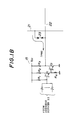
- FIG.1 B is a circuit diagram of the word driver/programming current absorbing circuit 15.
- the circuit configuration shown in FIG.1 B is provided for each of the word lines 22.
- the circuit in FIG.1 B is composed of two Schottky transistors 01 and Q2 and four resistors R1 - R4.
- the resistors R1 - R3 are connected to a power supply line maintained at a power supply voltage Vcc.
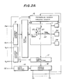
- each word line 22 with a programming current absorbing circuit 24 separately from a word driver 15A having the same configuration as that of the circuit 15 except for the transistor size.
- Each programming current absorbing circuit 24 is composed of a transistor Q3, a base current supply circuit 25, and a load resistor R7.
- the collector of the transistor Q3 is connected to the corresponding word line 22, and the base thereof is supplied with a base current generated by the base current supply circuit 25, which is connected to a power source line which is maintained at a programming voltage PV CE for use in data writing.
- the emitters of the transistors Q3 are maintained at a predetermined potential V A equal to, for example, ground potential GND.
- the collector of the transistors Q3 are coupled to the resistors R7 via the base current supply circuits 25.
- the transistors Q3 have sizes larger than the transistors Q2.
- the base current supply circuit 25 is composed of transistors Q4 and Q5, and resistors R5 - R8.
- the sizes of the transistors Q4 and Q5 are smaller than the size of the transistor Q3.
- the NPN type transistor Q4 and the PNP type transistor Q5 form an SCR (Silicon Controlled Rectifier).
- each word line 22 is not selected, it is maintained at a high potential approximately equal to Vcc, so that the transistor Q4 is OFF and thus the transistors Q3 and Q5 are also OFF.
- the transistor Q4 may be turned ON, and thus the transistors Q5 and Q3 are turned ON.
- the corresponding word line(s) is (are) turned ON, and data is erroneously written into the corresponding memory cell(s) 23.
- the word lines 21 do not have sufficient potential margins.
- a more specific object of the present invention is to provide a semiconductor memory device capable of definitely writing data into an only selected memory cell, so that the erroneous programming can be prevented.
- a programmable memory device comprising: memory cells arranged at cross points of word lines and bit lines; select means, coupled to the word lines, for selectively decreasing potentials of the word lines; write means, coupled to the bit lines, for selectively supplying programming currents to the memory cells via the bit lines; programming current absorbing transistors having first terminals respectively connected to the word lines, second terminals set at a predetermined potential, and bases; a common load element connected between a node and a programming voltage line; and a plurality of base current supplying means, respectively coupled to the programming current absorbing transistors and connected in common to the node, for turning ON the programming current absorbing transistors related to word lines selected by the select means so that base currents pass from the programming voltage line to the bases of the programming current absorbing transistors via the common load element and the base current supplying means.
- a programmable memory device comprising: memory cells arranged at cross points of word lines and bit lines; select means, coupled to the word lines, for selectively decreasing potentials of the word lines, the word lines being grouped into a plurality of groups; write means, coupled to the bit lines, for selectively supplying programming currents to the memory cells via the bit lines; programming current absorbing transistors having first terminals respectively connected to the word lines, second terminals set at a predetermined potential, and bases; a plurality of common load elements respectively provided with respect to the groups and connected between a programming voltage line and respective nodes; and a plurality of base current supplying means, respectively coupled to the programming current absorbing transistors and connected in common to the respective nodes, for turning ON the programming current absorbing transistors related to word lines selected by the select means so that base currents pass from the programming voltage line to the bases of the programming current absorbing transistors via the common load element and the base current supplying means.
- a programming current absorbing circuit 40 is substituted for the aforementioned programming current absorbing circuits 24 shown in FIGS.2A through 2C.
- memory cells 23-1 through 23-m are connected to a bit line 21-1, and connected to the word lines 22-1 through 22-m, respectively.
- m x n memory cells are provided at cross points of bit lines 21-1 through 21-m and word lines 22-1 through 22-m.
- Each memory cell is, for example, a fuse type or PN junction shortcircuiting memory cell.
- the programming current absorbing circuit 40 prevents large programming currents from passing through transistors Q21 through Q2m of the word driver 15A.
- the programming current absorbing circuit 40 is composed of NPN transistors Q31 - Q3m, base current supply circuits 51 - 5m, and a common load element 60. It should be noted that the common load element 60 is provided in common to the base current supply circuits 51 - 5m.
- the collectors of the transistors Q31 - Q3m are connected to word lines 22-1 - 22-m, respectively.
- the emitters of the transistors Q31 - Q3m are maintained at the predetermined potential V A lower than Vcc and PV CE , and the bases thereof are connected to the base current supply circuits 51 - 5m.
- the programming voltage PV CE is applied, via the common load element 60, to the base current supply circuits 51 - 5m.
- the collectors of the transistors Q31 - Q3m are coupled, via circuit elements of the circuits 51 - 5m, to a node A where one end of the common load element 60 is commonly connected to the base current supply circuits 51 - 5m.
- the word line 22-1 when the word line 22-1 is selected, the potential thereof becomes equal to the predetermined potential V A .
- the base current supply circuit 51 related to the selected word line 22-1 is turned ON, and the transistor Q31 is turned ON.
- most of the programming current passes through the bit line 21-1, the memory cell 23-1, the word line 22-1 and the transistor Q31.
- the potential of the node A is much lower than the programming voltage PV CE .
- the base current supply circuit 5m will not be turned ON because the potential of the node A is much lower than the programming voltage PV CE and insufficient to turn ON the base current supply circuit 5m.
- FIG.5A shows a first circuit configuration of the base current supply circuit 51.
- Each of the other base current supply circuits 52 - 5m has the same circuit configuration as the base current supply circuit 51.
- the base current supply circuit 51 is composed of a PNP transistor Q6 and a resistor R10.
- the emitter of the transistor Q6 is connected to the node A, and the base thereof is connected to the collector of the transistor Q31.
- the collector of the transistor Q6 is connected to the base of the transistor Q31 and one end of the resistor R10, the other end of which is grounded.
- FIG.5B shows a second circuit configuration of the base current supply circuit 51.
- Each of the other base current supply circuits 52 - 5m has the circuit configuration shown in FIG.5B.
- the base current supply circuit 51 is composed of a PNP transistor Q6 and an NPN transistor Q8, both forming a Darlington pair, and resistors R11 and R12.
- the emitter of the transistor Q6 and the collector of the transistor Q8 are connected to the node A.
- the base of the transistor Q6 is coupled to the collector of the transistor Q31 via the resistor R12.
- the collector of the transistor Q6 is connected to the base of the transistor Q8.
- the emitter of the transistor Q8 is connected to the base of the transistor Q31 and one end of the resistor R11. The other end of the resistor R11 is grounded.
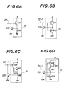
- FIG.6A shows a third circuit configuration of the base current supply circuit 51.
- Each of the other base current supply circuits 52 - 5m has the circuit configuration shown in FIG.6A.
- the third circuit configuration of the base current supply circuit 51 includes a P-channel field effect transistor Q9, and a resistor R13.
- the source of the transistor Q9 is connected to the node A, and the drain thereof is connected to the base of the transistor Q31 and one end of the resistor R13. The other end of the resistor R13 is grounded.
- the gate of the transistor Q9 is connected to the collector of the transistor Q31.
- FIG.6B shows a fourth circuit configuration of the base current supply circuit 51.
- Each of the other base current supply circuits 52 - 5m has the same circuit configuration as the circuit 51.
- the fourth circuit configuration includes an N-channel field effect transistor Q10 in addition to the P-channel field effect transistor Q9.
- the transistor Q10 functions as the resistor R13 shown in FIG.6A.
- the drain of the transistor Q9 is connected to the drain of the transistor Q10, and the source of the transistor Q10 is grounded.
- the gate of the transistor Q10 is connected to the collector of the transistor Q31.
- FIG.6C shows a fifth circuit configuration of the base current supply circuit 51.
- Each of the other base current supply circuits 52 - 5m has the same circuit configuration as the circuit 51.
- the fifth circuit configuration is composed of transistor Q9, an NPN transistor Q10, and two resistors R14 and R15.
- the collector of the transistor Q10 is connected to the source of the transistor Q9.
- the base of the transistor Q10 is connected to the drain of the transistor Q9.
- the resistor R14 is connected between the base and emitter of the transistor Q10.
- the emitter of the transistor Q10 is connected to the base of the transistor Q31 and one end of the resistor R15.
- the other end of the resistor R15 is grounded.
- the resistors R14 and R15 are load elements of the transistor Q9.
- FIG.6D shows a sixth circuit configuration of the base current supply circuit 51.
- Each of the other base current supply circuits 52 - 5m has the same circuit configuration as the circuit 51.
- the sixth circuit configuration includes four transistors Q9, Q10, Q11 and Q12.
- the transistors Q11 and Q12 which are N-channel field effect transistors, function as the resistors R14 and R15 shown in FIG.6C, respectively.
- the drain of the transistor Q11 is connected to the base of the transistor Q10, and the gate of the transistor Q11 is connected to the collector of the transistor Q31.
- the source of the transistor Q11 is connected to the base of the transistor Q31, the drain of the transistor Q12 and the emitter of the transistor Q10.
- the gate of the transistor Q12 is connected to the gate of the transistor Q9, and the source of the transistor Q12 is grounded.
- the word driver 15A receives the address signal from the address buffer 12, and turns ON at least one of the transistors Q21 through Q2m. At this time, it is possible to start to apply the programming voltage PV CE generated by an external device to the PROM. Assuming now that the selected word line is the word line 22-1, the potential of the word line 22-1 decreases to the potential V A , while the programming voltage PV CE is applied to the base current supply circuits 51 - 5m via the common resistor 60.
- each of the base current supply circuits 51 - 5m has the circuit configuration shown in FIG.5A
- the transistor Q6 of the base current supply circuit 51 related to the selected word line 22-1 is turned ON.
- the collector current of the transistor Q6 passes through the resistor R10 and is supplied to the base of the transistor Q31, so that the transistor Q31 is turned ON.
- the word line 22-1 is set to the potential V A via the transistors Q31 and the transistor Q21.
- the transistor Q6 is turned ON in response to the decrease in the potential of the word line 22-1.
- the collector current of the transistor Q6 passes through the transistor Q8 and the resistor R11, and is applied to the base of the transistor Q31. Thereby, the transistor Q31 is turned ON, so that the selected word line 22-1 is set to the potential V A via the transistors Q21 and Q31.
- each of the base current supply circuits 51 - 5m has any of the circuit configurations shown in FIGS.6A through 6D, the transistor Q31 is turned ON in response to the decrease in the potential of the selected word line 22-1.
- the programming current applying circuit 16 outputs the programming current to at least one of the bit lines 21-1 through 21-m. Assuming that the programming current applying circuit 16 supplies the programming current to the bit line 21-1, the programming current passes through the memory cell 23-1 and is applied to the selected word line 22-1. Sine the transistor Q31 has a size larger than that of the transistor Q21 and thus an ON resistance much lower than that of the transistor Q21, most of the programming current passes through the transistor Q31, and a very small amount of the programming current passes through the transistor Q21. When the programming (write) operation is completed, the transistor Q21 is turned OFF. At this time, the programming voltage PV CE supplied from the external device is turned OFF. The potential of the word line 22-1 starts to increase, and then the transistor Q31 is turned OFF.
- the node A is fixed to a potential lower than the programming voltage PV CE , and equal to, for example, 0.9V.
- the transistor Q6 shown in FIG.5A is not turned ON when the word line 22-m decreases to a potential insufficient to turn ON the transistor Q6.
- the transistor Q6 is not turned ON until the word line 22-m decreases to a potential equal to or lower than 0.1 V.
- the node A is fixed at, for example, 1.7V since the transistor Q8 is added to the circuit configuration shown in FIG.5A.
- the transistor Q6 related to the non-selected word line 22-m is not turned ON until it decreases to a potential equal to or lower than 0.9V.
- the transistors Q9 are not turned ON when the non-selected word line instantaneously decreases due to the occurrence of a noise.
- the first embodiment of the present invention operates as follows.
- the word driver 15A selects at least one of the word lines 22-1 through 22-m in accordance with the row address signal from the address buffer 12, and the sense amplifier 17 selects at least one of the bit lines 21-1 through 21-m in accordance with the column address signal from the address buffer 13.
- the programming voltage PV CE is not applied to the common load element 60.
- a read current generated by the sense amplifier 17 is applied to the selected memory cell, and data stored therein is read out therefrom.
- the readout data is sensed and amplified by the sense amplifier 17, and output to an external device via the output buffer 18.
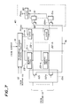
- FIG.7 is a circuit diagram of a second preferred embodiment of the present invention.
- the second embodiment of the present invention is configured by adding load elements 81 - 8m and a control line 82.
- the load elements 81 - 8m are connected to the control line 82 and the word lines 22-1 through 22-m, respectively.
- a programming voltage PV CEH is externally applied to the control line 82. It is preferable that PV CEH be larger than a programming voltage PV CEL which is applied to the common load element 60. During the programming operation, the programming voltage PV CEH is applied to the load elements 31 through 3m.
- the potential of the selected word line decreases to the voltage V A , while the non-selected word lines are pulled to a high potential by the programming voltage PV CEH in the state where the potential of the node A is much lower than the programming voltage PV CEL .
- the transistor Q6 (FIGS.5A and 5B) or Q9 (FIGS.6A through 6D) to turn ON due to the occurrence of a noise.
- FIG.8 is a block diagram of a third preferred embodiment of the present invention.
- the programming current absorbing circuit 40 shown in FIG.3 is divided into programming current absorbing circuits 40A and 40B.
- the programming current absorbing circuit 40A is provided for, for example, m/2 word lines, and the programming current absorbing circuit 40B is provided for the remaining m/2 word lines.
- Each of the circuits 40A and 40B is configured in the same way as the circuit 40A.
- the circuit 40A can prevent the erroneous programming operation arising from a noise on one or more word lines connected to the circuit 40A.
- the circuit 40B can prevent the erroneous programming operation arising from a noise on one or more word lines connected to the circuit 40B. It is possible to divide the circuit 40 shown in FIG.3 into three or more circuits. It will be noted the programming is more liable to be affected by noise as the circuit 40 is divided into an increased number of groups.
- FIG.9A shows the common load element 60.
- the common load element 60 is a resistor.
- the common load element 60 can be formed of a P-channel field effect transistor having a source connected to the PV CE line, a drain connected to the node A, and a grounded connected to the PV CE line.
- the common load element 60 can be formed of an N-channel field effect transistor having a drain connected to the PV CE line, a source connected to the node A, and a grounded gate shown in FIGS.4 and 7.
Landscapes
- Read Only Memory (AREA)
Applications Claiming Priority (2)
| Application Number | Priority Date | Filing Date | Title |
|---|---|---|---|
| JP2231515A JPH04113596A (ja) | 1990-08-31 | 1990-08-31 | 半導体記憶装置 |
| JP231515/90 | 1990-08-31 |
Publications (2)
| Publication Number | Publication Date |
|---|---|
| EP0473151A2 true EP0473151A2 (fr) | 1992-03-04 |
| EP0473151A3 EP0473151A3 (en) | 1993-06-02 |
Family
ID=16924699
Family Applications (1)
| Application Number | Title | Priority Date | Filing Date |
|---|---|---|---|
| EP19910114531 Withdrawn EP0473151A3 (en) | 1990-08-31 | 1991-08-28 | Programmable memory device having programming current absorbing transistors |
Country Status (3)
| Country | Link |
|---|---|
| US (1) | US5268864A (fr) |
| EP (1) | EP0473151A3 (fr) |
| JP (1) | JPH04113596A (fr) |
Families Citing this family (2)
| Publication number | Priority date | Publication date | Assignee | Title |
|---|---|---|---|---|
| JP2006203098A (ja) * | 2005-01-24 | 2006-08-03 | Sharp Corp | 不揮発性半導体記憶装置 |
| JP4054347B2 (ja) | 2005-12-16 | 2008-02-27 | シャープ株式会社 | 不揮発性半導体記憶装置 |
Family Cites Families (3)
| Publication number | Priority date | Publication date | Assignee | Title |
|---|---|---|---|---|
| JPS63104290A (ja) * | 1986-10-21 | 1988-05-09 | Nec Corp | 半導体記憶装置 |
| JPH0229998A (ja) * | 1988-07-19 | 1990-01-31 | Nec Corp | プログラマブル・リード・オンリー・メモリ |
| JPH02105395A (ja) * | 1988-10-13 | 1990-04-17 | Nec Corp | プログラマブル・リード・オンリー・メモリ |
-
1990
- 1990-08-31 JP JP2231515A patent/JPH04113596A/ja active Pending
-
1991
- 1991-08-28 US US07/751,107 patent/US5268864A/en not_active Expired - Fee Related
- 1991-08-28 EP EP19910114531 patent/EP0473151A3/en not_active Withdrawn
Also Published As
| Publication number | Publication date |
|---|---|
| EP0473151A3 (en) | 1993-06-02 |
| US5268864A (en) | 1993-12-07 |
| JPH04113596A (ja) | 1992-04-15 |
Similar Documents
| Publication | Publication Date | Title |
|---|---|---|
| US4608672A (en) | Semiconductor memory | |
| JPS606040B2 (ja) | 集積回路 | |
| JPS62189700A (ja) | プログラム可能なメモリ・マトリクス | |
| US4984207A (en) | Semiconductor memory device | |
| US4387449A (en) | Programmable memory device having reduced power consumption upon unselection | |
| EP0019381B1 (fr) | Mémoire à semi-conducteurs avec mise à niveau des signaux d'adresses | |
| US4432070A (en) | High speed PROM device | |
| US4806793A (en) | Signature circuit responsive to an input signal | |
| JPS5856286B2 (ja) | 出力バッファ回路 | |
| US5268864A (en) | Programmable memory device having programming current absorbing transistors | |
| US3972003A (en) | High speed current detection amplifier circuit | |
| US5359553A (en) | Low power ECL/MOS level converting circuit and memory device and method of converting a signal level | |
| EP0130414B1 (fr) | Mémoire de table de matières | |
| JPS582437B2 (ja) | スリ−ステイト出力回路 | |
| US4196363A (en) | Open collector bit driver/sense amplifier | |
| US5706236A (en) | Semiconductor memory device | |
| JPS5855597B2 (ja) | 双安定半導体メモリセル | |
| US4972375A (en) | Programmable semiconductor memory circuit | |
| US5734275A (en) | Programmable logic device having a sense amplifier with virtual ground | |
| US4964081A (en) | Read-while-write ram cell | |
| JPS62129996A (ja) | 可変行励振を有するメモリセル | |
| US5397935A (en) | Bias current supplying circuit | |
| JP2792256B2 (ja) | 半導体メモリ | |
| US4859874A (en) | PLA driver with reconfigurable drive | |
| US5396462A (en) | Semiconductor memory device having a data-lines clamp circuit |
Legal Events
| Date | Code | Title | Description |
|---|---|---|---|
| PUAI | Public reference made under article 153(3) epc to a published international application that has entered the european phase |
Free format text: ORIGINAL CODE: 0009012 |
|
| AK | Designated contracting states |
Kind code of ref document: A2 Designated state(s): DE FR GB |
|
| PUAL | Search report despatched |
Free format text: ORIGINAL CODE: 0009013 |
|
| AK | Designated contracting states |
Kind code of ref document: A3 Designated state(s): DE FR GB |
|
| 17P | Request for examination filed |
Effective date: 19931130 |
|
| STAA | Information on the status of an ep patent application or granted ep patent |
Free format text: STATUS: THE APPLICATION IS DEEMED TO BE WITHDRAWN |
|
| 18D | Application deemed to be withdrawn |
Effective date: 19960301 |