EP0475079B1 - Transformateur de retour - Google Patents
Transformateur de retour Download PDFInfo
- Publication number
- EP0475079B1 EP0475079B1 EP91113270A EP91113270A EP0475079B1 EP 0475079 B1 EP0475079 B1 EP 0475079B1 EP 91113270 A EP91113270 A EP 91113270A EP 91113270 A EP91113270 A EP 91113270A EP 0475079 B1 EP0475079 B1 EP 0475079B1
- Authority
- EP
- European Patent Office
- Prior art keywords
- inner frame
- outer case
- circuit board
- case
- focus
- Prior art date
- Legal status (The legal status is an assumption and is not a legal conclusion. Google has not performed a legal analysis and makes no representation as to the accuracy of the status listed.)
- Expired - Lifetime
Links
- 229920005989 resin Polymers 0.000 claims description 19
- 239000011347 resin Substances 0.000 claims description 19
- 238000005266 casting Methods 0.000 description 14
- 238000004519 manufacturing process Methods 0.000 description 4
- 230000015572 biosynthetic process Effects 0.000 description 3
- 230000003247 decreasing effect Effects 0.000 description 3
- WABPQHHGFIMREM-UHFFFAOYSA-N lead(0) Chemical compound [Pb] WABPQHHGFIMREM-UHFFFAOYSA-N 0.000 description 3
- 239000002184 metal Substances 0.000 description 3
- 238000000034 method Methods 0.000 description 2
- 238000005192 partition Methods 0.000 description 2
- 239000004721 Polyphenylene oxide Substances 0.000 description 1
- 238000011161 development Methods 0.000 description 1
- 230000018109 developmental process Effects 0.000 description 1
- 238000010894 electron beam technology Methods 0.000 description 1
- 239000003822 epoxy resin Substances 0.000 description 1
- 238000002347 injection Methods 0.000 description 1
- 239000007924 injection Substances 0.000 description 1
- 238000000465 moulding Methods 0.000 description 1
- -1 polybutylene terephthalate Polymers 0.000 description 1
- 229920001707 polybutylene terephthalate Polymers 0.000 description 1
- 229920000647 polyepoxide Polymers 0.000 description 1
- 229920006380 polyphenylene oxide Polymers 0.000 description 1
- 238000004804 winding Methods 0.000 description 1
Images


Classifications
-
- H—ELECTRICITY
- H01—ELECTRIC ELEMENTS
- H01F—MAGNETS; INDUCTANCES; TRANSFORMERS; SELECTION OF MATERIALS FOR THEIR MAGNETIC PROPERTIES
- H01F38/00—Adaptations of transformers or inductances for specific applications or functions
- H01F38/42—Flyback transformers
-
- H—ELECTRICITY
- H01—ELECTRIC ELEMENTS
- H01F—MAGNETS; INDUCTANCES; TRANSFORMERS; SELECTION OF MATERIALS FOR THEIR MAGNETIC PROPERTIES
- H01F38/00—Adaptations of transformers or inductances for specific applications or functions
- H01F38/42—Flyback transformers
- H01F2038/423—Flyback transformers with adjusting potentiometers
Definitions
- the present invention relates to a flyback transformer having a focus pack.
- a high voltage is required.
- a flyback transformer which generates a high voltage by utilizing a flyback pulse is used.
- a flyback transformer generates and applies a high voltage (e.g., 25 kV) to the anode of a cathode-ray tube. This high voltage is also appropriately decreased across a resistor to obtain a focus voltage (e.g., 10 kV) to be applied to an electron beam focusing electrode arranged in an electron gun, and a screen voltage (e.g., 1 kV) to be applied to a screen electrode for color adjustment.
- a high voltage e.g., 25 kV
- This high voltage is also appropriately decreased across a resistor to obtain a focus voltage (e.g., 10 kV) to be applied to an electron beam focusing electrode arranged in an electron gun, and a screen voltage (e.g., 1 kV) to be applied to a screen electrode for color adjustment.
- a focus pack In order to obtain a focus voltage and a screen voltage from a high voltage generated by a flyback transformer, a unit called a focus pack is used.
- Japanese Patent Laid-Open JP-A-2-28905 proposes a flyback transformer having a focus pack.
- an inner case 3 is fitted inside an outer case 2 to constitute a focus pack 1 as a double case.
- a rotational operation shaft 5 of the variable resistor extends from a shaft retaining cylinder 6 of the inner case 3 to the outside to be freely rotatable.
- the outer case 2 of this focus pack 1 is fitted on a transformer case 7.
- the transformer case 7 is filled with an insulating casting resin 8 to insulate the circuit board 4 by the inner case 3, the insulating casting resin 8, and the outer case 2.
- an insulating casting resin 8 to insulate the circuit board 4 by the inner case 3, the insulating casting resin 8, and the outer case 2.
- electrical discharge from a high-voltage portion of the circuit board 4 to the outside is prevented.
- Reference numeral 11 denotes a low-voltage coil housed in the transformer case 7; 13, a high-voltage coil; and 15, a core.
- Japanese Utility Model Laid-Open JP-A-2-65304 proposes a focus pack having a double case structure.
- a focus pack 1 is constituted by outer and inner cases 2 and 3, and shaft retaining cylinders 6 on the inner case 3 side, in which rotational operation shafts 5 for focus and screen adjusting variable resistors extend, are hermetically fitted in the holes in the outer case 2, thereby integrating the cases 2 and 3.
- the high-voltage portion of a circuit board 4 is insulated by the double case, in the same manner as described above, thereby preventing electrical discharge from the high-voltage portion to the outside.
- the outer and inner cases 2 and 3 are separately formed, and are integrated during assembly by fitting the shaft retaining cylinder 6 of the inner case 3 side into the hole in the outer case 2. Therefore, the outer and inner cases 2 and 3 must be formed in separate steps by using separate molds, and the cases 2 and 3 formed in the separate steps must be integrated by fitting, resulting in cumbersome procedures. As a result, the work efficiency in the manufacture of the apparatus is low, resulting in an increase in cost of the apparatus.
- the present invention has been made to resolve the problems described above, and has as its object to eliminate the cumbersomeness of forming outer and inner cases of a focus pack in separate steps by using separate molds and integrally fitting the outer and inner cases, thereby providing a flyback transformer of a high work efficiency.
- the object is solved by the features of claim 1, relating to a flyback transformer as well as claim 4, relating to a focus pack.
- the subclaims describe further positive developments of the features of claim 1.
- the present invention provides a flyback transformer constituted such that a focus pack incorporating a circuit board having a resistor circuit including a variable resistor for focus voltage supply is mounted on a transformer case, comprising an outer case to be mounted on the transformer case, and an inner frame, formed inside the outer case to be integral with the outer case, for incorporating the circuit board, wherein an opening path is formed between the outer case and the inner frame, a shaft hole extending through the opening path is provided for the outer case and the inner frame, the shaft hole is defined from the opening path by an insulating cylinder wall, and a rotational operation shaft for the variable resistor is inserted in a cylinder hole of the insulating cylinder wall.
- the outer case and the inner frame of the focus pack are integrally formed.
- the opening path is formed between the outer case and the inner frame.
- the circuit board having the resistor circuit formed thereon is housed in the inner frame, and the rotational operation shaft of the variable resistor is inserted in the shaft hole defined by the insulating cylinder wall.
- the focus pack is mounted on the transformer case, and the transformer case is filled with an insulating casting resin.
- the insulating casting resin flows into the opening path defined between the outer case and the inner frame, and the circuit board is insulated from the outside by the inner frame, the insulating casting resin, and the outer case.
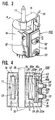
- Fig. 3 shows an outer appearance of the flyback transformer according to the present invention
- Fig. 4 is a sectional view taken along the line A - A of Fig. 3.
- a low-voltage coil 11 is wound around a low-voltage coil bobbin 10, and a high-voltage coil 13 is wound around a high-voltage coil bobbin 12 arranged around the low-voltage coil 11.
- This assembly is housed in a transformer case 14, the transformer case 14 is filled with an insulating casting resin 8, and a core 15 is inserted at the center of the low-voltage coil bobbin 10.
- an outer case 16 of a focus pack 100 is fitted to a portion of the transformer case 14.
- a screen lead wire 18 and a focus lead wire 19 extend from the lower and upper portions, respectively, of the focus pack 100.
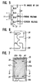
- the low- and high-voltage coils 11 and 13 serve as primary and secondary windings, respectively.
- the high-voltage coil 13 is divided by a plurality of (4 in the case shown in Fig. 5) diodes D1 to D4.
- the high-voltage terminal of the high-voltage coil 13 is connected to the anode of a television receiver through a diode D5.
- a stationary resistor R, a variable resistor VR F for focus voltage adjustment, and a variable resistor VR S for screen voltage adjustment are connected in series between the high-voltage terminal and ground.
- the variable resistors VR F and VR S surrounded by a broken line are provided on a circuit board 35 to be described later.
- the outer case 16 of the focus pack 100 is made of an insulating resin such as a modified polyphenylene oxide and polybutylene terephthalate.
- a side 20 on the lower side of the outer case 16, and a flat 21 which is side of the outer case 16 are open.
- the terminal portion of the outer case 16 on the open flat 21 side forms a fitting portion 16a to be mounted on the transformer case 14.
- An inner frame 22 is formed on a bottom 16b side of the outer case 16 to be integral with the outer case 16 through a side wall pillar 22c.
- the inner frame 22 has a side wall 22a the flat of which is open.
- An opening path 23 is defined between a bottom 22b of the inner frame 22 and the bottom 16b of the outer case 16, and between a side wall 16c of the outer case 16 on the opposite side of the open side 20 and the side wall 22a of the inner frame 22 which is adjacent to the side wall 16c.
- the opening path 23 is continuous from the side wall 16c side to the bottom 16b side.
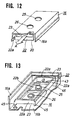
- the opening path 23 is formed in the following manner. Metal frames (not shown) are inserted in the bottom 22b and the side wall 22a side of the inner frame 22 to perform molding. When the molded products are to be released from the metal molds, the metal frames are slid in directions A and B, respectively (Fig. 11), thereby forming the opening path 23.
- Shaft holes 25 and 26 are provided for the outer case 16 and the inner frame 22, and retaining cylinders 28 and 29 having flanges 27 are inserted in the shaft holes 25 and 26, respectively.
- cylinder holes 30 and 31 of the retaining cylinders 28 and 29 are defined by the cylinder walls (insulating cylinder walls) of the retaining cylinders 28 and 29.
- a focus rotational operation shaft 32 for focus voltage adjustment is rotatably fitted in the cylinder hole 30 of the retaining cylinder 28, and a screen rotational operation shaft 33 for screen voltage adjustment is rotatably inserted in the cylinder hole 31 of the retaining cylinder 29.
- the circuit board 35 is mounted on the opening flat surface side of the inner frame 22.
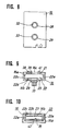
- the resistor circuit (not shown) including focus variable resistor VR F for changing the focus voltage and the screen variable resistor VR S for changing the screen voltage are formed on the circuit board 35, as shown in Fig. 6.
- a slider 36 for sliding on the focus variable resistor VR F is provided on the bottom of the focus rotational operation shaft 32, and a slider 37 for sliding on the screen variable resistor VR S is provided on the bottom of the screen rotational operation shaft 33.
- a focus voltage output terminal 38 for outputting the focus voltage, a screen voltage output terminal 39 for outputting the screen voltage, an input terminal 40 for supplying a high voltage from the high-voltage coil 13 to the resistor circuit and a ground terminal 41 of the resistor circuit are provided on the remaining surface of the circuit board 35.
- the focus pack 100 having the above arrangement is mounted on the transformer case 14 of the flyback transformer by fitting the fitting portion 16a of the outer case 16 on the mounting portion of the transformer case 14, as shown in Fig. 4.
- the insulating casting resin 8 such as an epoxy resin is injected into the transformer case 14.
- the insulating casting resin 8 flows into the opening path 23.
- the circuit board 35 is insulated from the outside by the inner frame 22. Consequently electrical discharge from the high-voltage portion of the resistor circuit to the outside is reliably prevented.
- a partition 43 blocks the insulating casting resin 8 from entering into the cylinder holes 30 and 31.
- the partition 43 supports it to be kept at a predetermined gap from the bottom 22b of the inner frame 22.
- the outer case 16 and the inner frame 22 of the focus pack 100 are integrally formed by a single mold in a single formation step.
- the cumbersome work steps of apparatuses conventionally proposed, i.e., forming the outer and inner cases 2 and 3 in separate steps by using separate molds and then integrating the cases 2 and 3 by fitting them, can be omitted.
- workability of the manufacture of the apparatus is greatly improved, and the manufacturing cost is decreased.
- the inner frame 22 is integrally formed inside the outer case 16, unlike in the conventional apparatus in which the cases 2 and 3 are fitted to obtain a double structure.
- the two types of cases 2 and 3 having different sizes are fitted.
- the size and shape of each fitting portion with respect to the transformer case can be more easily made identical to those of the existing focus pack which is formed of a single outer case.
- the focus pack of this embodiment can be mounted in an existing flyback transformer, and the conventional flyback transformer having the focus pack can be easily replaced by a flyback transformer having the focus pack of this embodiment.
- Fig. 13 is a perspective view of a focus pack constituting a second embodiment of the flyback transformer according to the present invention.
- the second embodiment is different from the first embodiment in the following respects.
- a side wall pillar 45 of an inner frame 22, that couples an outer case 16 and the inner frame 22 of a focus pack 100, is not formed in the entire region of the side wall 22a of the inner frame 22 in the longitudinal direction. Rather, the side wall pillar 45 is provided to extend from an end portion of the side wall 22a to a substantially intermediate position, and the side wall pillar 45 is not formed in the remaining region extending from the substantially intermediate portion to the other end portion of the side wall 22a. Hence, a complete space 46 is provided between the bottom 22b of the inner frame 22 and the bottom 16b of the outer case 16.
- the present invention is not limited to the embodiments described above but can be modified in various manners.
- the focus pack 100 is mounted on the transformer case 14, and thereafter the transformer case 14 is filled with the insulating casting resin 8 to flow into the opening path 23.
- injection of the insulating casting resin 8 into the opening path 23 can be performed prior to mounting of the focus pack 100 to the transformer case 14 of the flyback transformer.
- the insulating resin 42 to cover the circuit board 35 can be replaced by the insulating casting resin 8. Then, insulating coverage is performed simultaneously when the insulating casting resin 8 is charged into the opening path 23.
- the outer case and the inner frame are integrally formed to constitute the focus pack. Therefore, the outer case and the inner frame can be integrally formed in a single formation step by using a single mold. As a result, compared to the method of the conventionally proposed apparatuses in which the outer and inner cases are formed in separate steps by using separate molds and are fitted to each other in the assembly step, the manufacturing work efficiency is greatly improved while the cost is greatly decreased.
- the high-voltage portion of the circuit board housed in the inner frame is insulated from the outside by the inner frame, the insulating resin injected in the opening path, and the outer case. Therefore, the dielectric strength of the high-voltage portion is increased, and electrical discharge from the circuit board to the outside can be reliably prevented.
Landscapes
- Engineering & Computer Science (AREA)
- Power Engineering (AREA)
- Coils Or Transformers For Communication (AREA)
- Details Of Television Scanning (AREA)
- Apparatuses And Processes For Manufacturing Resistors (AREA)
Claims (4)
- Transformateur de retour de spot avec une unité de focalisation (100) montée sur un boîtier de transformateur (14), ladite unité de focalisation contenant une carte de circuit (35) ayant un circuit de résistance, qui comprend une résistance variable (VRF, VRS) destinée à fournir une tension de focalisation et montée sur celle-ci, ladite unité de focalisation comprenant :
un boîtier extérieur (16) monté sur ledit boîtier de transformateur et un châssis intérieur (22) pour incorporer ladite carte imprimée, ledit châssis intérieur étant formé à l'intérieur du boîtier extérieur, en étant solidaire, et étant supporté sur un pilier de paroi latérale (22c) afin de former un chemin d'ouverture (23) entre ledit boîtier extérieur et ledit châssis intérieur (22) qui est continu d'un côté dudit châssis intérieur (22) à l'autre côté de celui-ci ;
un trou d'arbre (25, 26) s'étendant à travers ledit boîtier extérieur (16) et ledit châssis intérieur (22) ;
un cylindre de retenue (28, 29) inséré dans ledit trou d'arbre ; et
un arbre de commande rotatif (32, 33) destiné à ajuster ladite résistance variable (VRF, VRS) sur ladite carte de circuit (35), ledit arbre étant disposé dans le trou de cylindre du cylindre de retenue. - Transformateur de retour de spot selon la revendication 1, dans lequel :
ledit circuit de résistance a une deuxième résistance variable destinée à fournir une tension d'écran formée à l'intérieur de celle-ci,
un deuxième trou d'arbre est prévu, qui s'étend à travers le boîtier extérieur (16) et ledit châssis intérieur (22), un deuxième cylindre de retenue est inséré dans ledit deuxième trou d'arbre, et
un deuxième arbre de commande rotatif, pour ajuster ladite deuxième résistance variable sur ladite carte de circuit (35), est disposé dans le trou de cylindre du deuxième cylindre de retenue. - Transformateur de retour de spot selon les revendications 1 ou 2, dans lequel un pilier de paroi latérale (22c) supportant ledit châssis intérieur (22) sur ledit boîtier extérieur (16) fait la moitié de la longueur d'une paroi latérale (22a) dudit châssis intérieur (22).
- Unité de focalisation comprenant un boîtier extérieur (16) et un châssis intérieur (22) pour incorporer une carte de circuit (35), ledit châssis intérieur (22) étant formé à l'intérieur dudit boîtier extérieur (16), en étant solidaire, et étant porté sur un pilier de paroi latérale (22c) de manière à former un chemin d'ouverture (23) entre ledit boîtier extérieur (16) et ledit châssis intérieur (22), chemin qui est continu d'un côté dudit châssis intérieur (22) à l'autre côté de celui-ci ; une carte de circuit (35) logée dans ledit châssis intérieur (22) et ayant un circuit de résistance comprenant une résistance variable formée sur celui-ci ; un trou d'arbre (25, 26) s'étendant à travers ledit boîtier extérieur (16) et ledit châssis intérieur (22) ; un cylindre isolant (28, 29) passant à travers ledit trou d'arbre (25, 26) ; un arbre de commande rotatif (32, 33) pour ajuster ladite résistance variable sur ladite carte de circuit (35), ledit arbre étant disposé dans ledit cylindre isolant ; et un élément en résine isolant électriquement injecté et durci dans les espaces ouverts dudit boîtier extérieur (16) et dudit châssis intérieur (22).
Applications Claiming Priority (2)
| Application Number | Priority Date | Filing Date | Title |
|---|---|---|---|
| JP213927/90 | 1990-08-13 | ||
| JP2213927A JPH07118404B2 (ja) | 1990-08-13 | 1990-08-13 | フライバックトランスおよびその製造方法 |
Publications (2)
| Publication Number | Publication Date |
|---|---|
| EP0475079A1 EP0475079A1 (fr) | 1992-03-18 |
| EP0475079B1 true EP0475079B1 (fr) | 1995-11-15 |
Family
ID=16647351
Family Applications (1)
| Application Number | Title | Priority Date | Filing Date |
|---|---|---|---|
| EP91113270A Expired - Lifetime EP0475079B1 (fr) | 1990-08-13 | 1991-08-07 | Transformateur de retour |
Country Status (5)
| Country | Link |
|---|---|
| US (1) | US5160872A (fr) |
| EP (1) | EP0475079B1 (fr) |
| JP (1) | JPH07118404B2 (fr) |
| KR (1) | KR0129005B1 (fr) |
| DE (1) | DE69114628T2 (fr) |
Families Citing this family (10)
| Publication number | Priority date | Publication date | Assignee | Title |
|---|---|---|---|---|
| JPH04120212U (ja) * | 1991-04-15 | 1992-10-27 | 株式会社村田製作所 | フライバツクトランス |
| FR2726686B1 (fr) * | 1994-11-07 | 1996-12-20 | Thomson Television Components | Transformateur haute tension a redressement fractionne avec diodes regroupees |
| JPH08236376A (ja) * | 1995-02-28 | 1996-09-13 | Murata Mfg Co Ltd | フライバックトランス |
| US5731959A (en) * | 1995-03-21 | 1998-03-24 | Lg Electronics Inc. | Resistor-printed board built in a flyback transformer for a video display appliance |
| JP2968940B2 (ja) * | 1996-02-26 | 1999-11-02 | エイサー ペリフェラルズ インコーポレイテッド | フライバック・パルス信号を形成するためのビルトイン・ピンを含むフライバック・トランス |
| DE19609656C1 (de) * | 1996-03-12 | 1997-07-24 | Acer Peripherals Inc | Klammervorrichtung für Ausgangsleitungen eines Horizontal-Ablenktransformators |
| JP3380679B2 (ja) * | 1996-05-08 | 2003-02-24 | アルプス電気株式会社 | 電気部品 |
| TW418409B (en) | 1999-10-14 | 2001-01-11 | Darfon Electronics Corp | Core engaging structure for flyback transformer |
| KR100415565B1 (ko) * | 2001-07-27 | 2004-01-24 | 삼성전기주식회사 | 플라이 백 트랜스 포머의 포커스 커버 |
| US20090108975A1 (en) * | 2006-05-08 | 2009-04-30 | Takesi Nomura | High-voltage transformer |
Family Cites Families (8)
| Publication number | Priority date | Publication date | Assignee | Title |
|---|---|---|---|---|
| JPS5938027Y2 (ja) * | 1979-05-02 | 1984-10-22 | 株式会社日立製作所 | フライバツクトランス |
| US4402037A (en) * | 1980-09-17 | 1983-08-30 | Murata Manufacturing Co., Ltd. | Cathode-ray tube socket substrate |
| CA1188819A (fr) * | 1981-06-30 | 1985-06-11 | Sanyo Electric Co., Ltd. | Transformateur de sortie horizontale |
| JPS6018904A (ja) * | 1983-07-12 | 1985-01-31 | Murata Mfg Co Ltd | 可変抵抗器付きフライバツクトランス |
| US4527229A (en) * | 1983-09-19 | 1985-07-02 | Murata Manufacturing Co., Ltd. | Flyback transformer with high voltage variable resistor built therein |
| DE3334904C1 (de) * | 1983-09-27 | 1984-06-20 | Murata Manufacturing Co., Ltd., Nagaokakyo, Kyoto | Zeilenendtransformator mit eingebautem variablem Hochspannungswiderstand |
| JPH0670926B2 (ja) * | 1987-05-18 | 1994-09-07 | 松下電器産業株式会社 | フライバツクトランス |
| JPH0268407U (fr) * | 1988-11-14 | 1990-05-24 |
-
1990
- 1990-08-13 JP JP2213927A patent/JPH07118404B2/ja not_active Expired - Fee Related
-
1991
- 1991-08-07 EP EP91113270A patent/EP0475079B1/fr not_active Expired - Lifetime
- 1991-08-07 DE DE69114628T patent/DE69114628T2/de not_active Expired - Fee Related
- 1991-08-12 KR KR1019910013887A patent/KR0129005B1/ko not_active Expired - Fee Related
- 1991-08-13 US US07/744,608 patent/US5160872A/en not_active Expired - Lifetime
Also Published As
| Publication number | Publication date |
|---|---|
| DE69114628D1 (de) | 1995-12-21 |
| DE69114628T2 (de) | 1996-04-18 |
| US5160872A (en) | 1992-11-03 |
| EP0475079A1 (fr) | 1992-03-18 |
| KR920005588A (ko) | 1992-03-28 |
| JPH0496302A (ja) | 1992-03-27 |
| KR0129005B1 (ko) | 1998-04-10 |
| JPH07118404B2 (ja) | 1995-12-18 |
Similar Documents
| Publication | Publication Date | Title |
|---|---|---|
| US4095206A (en) | Encapsulated transformer assembly | |
| EP0939412B1 (fr) | Composants inductifs et bobines composites correspondantes | |
| US5160872A (en) | Flyback transformer | |
| EP0886286B1 (fr) | Transformateur à haute tension et dispositif d'éclairage à lampe pour véhicule l'utilisant | |
| US6215385B1 (en) | Ignition coil with primary winding outside of secondary winding | |
| US5138290A (en) | Deflection yoke | |
| EP0379641A1 (fr) | Dispositif de bobine d'allumage pour machine à combustion interne | |
| US4247889A (en) | High-voltage-secondary transformer, particularly television line transformer | |
| US5287479A (en) | Flyback transformer | |
| US6850143B2 (en) | Flyback transformer | |
| US4055825A (en) | Voltage transformer for high voltage | |
| US5289145A (en) | Electromagnetic relay and a method for its production | |
| US6463919B1 (en) | Ignition coil with polyimide case and/or secondary spool | |
| US20050161031A1 (en) | Electronic module for internal combustion engine ignition coil | |
| US6507131B1 (en) | High-voltage transformer | |
| US20020036560A1 (en) | Detachable transformer | |
| KR20000023456A (ko) | 고압 변압기 | |
| JPH075622Y2 (ja) | フライバックトランス | |
| US6255770B1 (en) | Corona resistant saddle-shaped deflection coil | |
| JP2570076Y2 (ja) | フライバックトランス | |
| CN1426074A (zh) | 回扫变压器和在该变压器中固定泄漏电阻的装置 | |
| JP2000260635A (ja) | トランス | |
| JP2621397B2 (ja) | フライバックトランス | |
| JPH0331058Y2 (fr) | ||
| US20040080390A1 (en) | Ignition coil and techniques for introducing encapsulating material therein |
Legal Events
| Date | Code | Title | Description |
|---|---|---|---|
| PUAI | Public reference made under article 153(3) epc to a published international application that has entered the european phase |
Free format text: ORIGINAL CODE: 0009012 |
|
| AK | Designated contracting states |
Kind code of ref document: A1 Designated state(s): DE GB IT |
|
| 17P | Request for examination filed |
Effective date: 19920622 |
|
| 17Q | First examination report despatched |
Effective date: 19940916 |
|
| GRAA | (expected) grant |
Free format text: ORIGINAL CODE: 0009210 |
|
| AK | Designated contracting states |
Kind code of ref document: B1 Designated state(s): DE GB IT |
|
| REF | Corresponds to: |
Ref document number: 69114628 Country of ref document: DE Date of ref document: 19951221 |
|
| ITF | It: translation for a ep patent filed | ||
| PLBE | No opposition filed within time limit |
Free format text: ORIGINAL CODE: 0009261 |
|
| STAA | Information on the status of an ep patent application or granted ep patent |
Free format text: STATUS: NO OPPOSITION FILED WITHIN TIME LIMIT |
|
| 26N | No opposition filed | ||
| REG | Reference to a national code |
Ref country code: GB Ref legal event code: IF02 |
|
| PGFP | Annual fee paid to national office [announced via postgrant information from national office to epo] |
Ref country code: GB Payment date: 20060802 Year of fee payment: 16 |
|
| PGFP | Annual fee paid to national office [announced via postgrant information from national office to epo] |
Ref country code: DE Payment date: 20060803 Year of fee payment: 16 |
|
| PGFP | Annual fee paid to national office [announced via postgrant information from national office to epo] |
Ref country code: IT Payment date: 20060831 Year of fee payment: 16 |
|
| GBPC | Gb: european patent ceased through non-payment of renewal fee |
Effective date: 20070807 |
|
| PG25 | Lapsed in a contracting state [announced via postgrant information from national office to epo] |
Ref country code: DE Free format text: LAPSE BECAUSE OF NON-PAYMENT OF DUE FEES Effective date: 20080301 |
|
| PG25 | Lapsed in a contracting state [announced via postgrant information from national office to epo] |
Ref country code: GB Free format text: LAPSE BECAUSE OF NON-PAYMENT OF DUE FEES Effective date: 20070807 |
|
| PG25 | Lapsed in a contracting state [announced via postgrant information from national office to epo] |
Ref country code: IT Free format text: LAPSE BECAUSE OF NON-PAYMENT OF DUE FEES Effective date: 20070807 |