EP0475345B1 - Dispositif convertisseur de puissance courant continu/courant alternatif - Google Patents
Dispositif convertisseur de puissance courant continu/courant alternatif Download PDFInfo
- Publication number
- EP0475345B1 EP0475345B1 EP91115268A EP91115268A EP0475345B1 EP 0475345 B1 EP0475345 B1 EP 0475345B1 EP 91115268 A EP91115268 A EP 91115268A EP 91115268 A EP91115268 A EP 91115268A EP 0475345 B1 EP0475345 B1 EP 0475345B1
- Authority
- EP
- European Patent Office
- Prior art keywords
- circuit
- signal
- switching
- cyclo
- inverter
- Prior art date
- Legal status (The legal status is an assumption and is not a legal conclusion. Google has not performed a legal analysis and makes no representation as to the accuracy of the status listed.)
- Expired - Lifetime
Links
Images


Classifications
-
- H—ELECTRICITY
- H02—GENERATION; CONVERSION OR DISTRIBUTION OF ELECTRIC POWER
- H02M—APPARATUS FOR CONVERSION BETWEEN AC AND AC, BETWEEN AC AND DC, OR BETWEEN DC AND DC, AND FOR USE WITH MAINS OR SIMILAR POWER SUPPLY SYSTEMS; CONVERSION OF DC OR AC INPUT POWER INTO SURGE OUTPUT POWER; CONTROL OR REGULATION THEREOF
- H02M7/00—Conversion of AC power input into DC power output; Conversion of DC power input into AC power output
- H02M7/42—Conversion of DC power input into AC power output without possibility of reversal
- H02M7/44—Conversion of DC power input into AC power output without possibility of reversal by static converters
- H02M7/48—Conversion of DC power input into AC power output without possibility of reversal by static converters using discharge tubes with control electrode or semiconductor devices with control electrode
- H02M7/4807—Conversion of DC power input into AC power output without possibility of reversal by static converters using discharge tubes with control electrode or semiconductor devices with control electrode having a high frequency intermediate AC stage
-
- H—ELECTRICITY
- H02—GENERATION; CONVERSION OR DISTRIBUTION OF ELECTRIC POWER
- H02M—APPARATUS FOR CONVERSION BETWEEN AC AND AC, BETWEEN AC AND DC, OR BETWEEN DC AND DC, AND FOR USE WITH MAINS OR SIMILAR POWER SUPPLY SYSTEMS; CONVERSION OF DC OR AC INPUT POWER INTO SURGE OUTPUT POWER; CONTROL OR REGULATION THEREOF
- H02M7/00—Conversion of AC power input into DC power output; Conversion of DC power input into AC power output
Definitions
- the present invention relates to a DC-to-AC electric power converting apparatus according to the preamble of claim 1.
- a DC-to-AC electric power converting apparatus is known from Intelec, 89 Conf. Proceedings, 15 Oct. 1989, FIRENZE Article 19.1, page 1-6, Muroyama : "A control method for a high frequency link inverter using cycloconverter techniques".
- the present invention relates to an electric power converting apparatus of a high frequency intermediate link system in which high frequency electric power is transmitted/received via an insulating transformer.
- Fig. 15 is a block diagram of a conventional DC-to-Ac power converting apparatus as disclosed in IEEE PESC '88 Record, pp658-663, 1988.
- reference numeral 1 represents an inverter circuit
- 2 represents a transformer the input of which is connected to the inverter circuit 1
- 3 represents a cyclo-converter circuit connected to the output of the transformer 2.
- Reference numeral 4 represents a filter circuit connected to the output of the cyclo-converter circuit 3 and 5 represents a current detector for detecting the output current from the cyclo-converter circuit 3.
- Reference numeral 6 represents a carrier signal generator, 7 represents a reference voltage signal generating circuit and 8 represents an absolute circuit.
- Reference numeral 9 represents a PWM circuit
- 10 represents an inverter switching circuit
- 11 represents a cyclo-converter switching circuit.
- the inverter circuit 1 comprises four semiconductor switching devices S1 to S4, while the cyclo-converter circuit 3 comprises four semiconductor switching devices S5, S6, S 5A and S 6A .
- the transformer 2 is arranged in such a manner that the turn ratio of the primary coil and the secondary coil is 1:2 and an intermediate tap is formed at the midpoint of the secondary coil.
- the filter circuit 4 is an LC filter circuit comprising a reactor and a capacitor.
- Reference numerals 12 and 13 respectively represent a DC power source and a load circuit connected to the DC-to-AC electric power converting apparatus.
- the binary signal T a the level of which is changed in synchronization with the timing at which the amplitude of the absolute signal
- the binary signal T b the level of which is changed in synchronization with the last transition of the carrier signal
- the binary signal T a and T b are supplied to the inverter switching circuit 10 so that ON/OFF signals T1 to T4 for switching on/off the four semiconductor switching devices S1 to S4 constituting the inverter circuit 1 are transmitted. That is, the ON/OFF signals T1 and T3 are the same as the binary signals T b and T a , respectively.
- the ON/OFF signals T2 and T4 are the signals obtained by respectively inverting the sign of the binary signals T b and T a .
- the level of the ON/OFF signals T1 to T4 is high, the corresponding semiconductor switching devices S1 to S4 are switched on.
- the corresponding semiconductor switching devices S1 to S4 are switched off.
- V2 becomes AC voltage the pulse width of which has been modulated as shown in Fig. 16.
- the cyclo-converter switching circuit 11 discriminates the polarity of the reference voltage signal V* and the output current i cc from the cyclo-converter circuit 3 respectively supplied from the reference voltage signal generating circuit 7 and the current detector 5.
- the ON/OFF signals T5, T6, T 5A and T 6A as shown in Fig. 16 are generated from the binary signal T b supplied from the PWM circuit 9 in accordance with the thus discriminated polarity.
- sine-wave voltage, the pulse width of which has been modulated and which is as shown in the lowermost portion of Fig. 16 can be obtained as the output voltage V cc from the cyclo-converter 3.
- the switch S 5A switches off the electric current
- the current commutates to the switch S 6A .
- the switch S4 switches off the electric current in a state where the electric current passes because the switches S1 and S4 are switched on, the electric current commutates to the switch S3 which is switched on.
- the conventional DC-to-AC electric power converting apparatus receives DC electric power and transmits AC electric power in accordance to the reference voltage signal.
- the above-described DC-to-AC electric power converting apparatus is usually called "a high frequency intermediate link type electric power converting apparatus" since the high frequency electric power is supplied/received via a transformer.
- a structure, in which the high frequency intermediate link type electric power converting apparatus is employed in an AC power source apparatus such as the uninterruptive power supply system will enable the size and the weight of the insulating transformer and the filter circuit to be reduced.
- the conventional DC/AC power converting apparatus encounters problems in that the conversion efficiency is unsatisfactory and the switching frequency cannot be raised due to large switching loss generated because the switching elements of the inverter circuit and the cyclo-converter circuit switch on/off the electric current. Furthermore, there arises another problem of generating voltage surge due to switching.
- an object of the present invention is to provide DC/AC power converting apparatus exhibiting small switching loss, high conversion efficiency and reduced voltage surge.
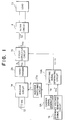
- Figs. 1 to 5 illustrate a first embodiment of the present invention, where Fig. 1 illustrates the structure of the first embodiment.
- reference numeral 2A represents a transformer
- 6A represents a carrier signal generator
- 14 represents an inverter circuit
- 15 represents a cyclo-converter circuit.
- Reference numeral 16 represents a reference voltage signal generating circuit
- 17A represents an inverter switching circuit.
- Reference numeral 18A represents a switching signal generating circuit.
- the filter circuit 4, the DC power source 12 and the load circuit 13 are the same as those for the conventional structure.
- Fig. 2 illustrates the detailed structure of each of the inverter circuit 14, the transformer 2A and the cyclo-converter circuit 15.
- the inverter circuit 14 comprises input terminals 141 and 142 connected to the DC power source 12, semiconductor switching devices S1 to S4 such as transistors and MOSFETs, diodes D1 to D4 connected to the respective switching devices S1 to S4 in an inverted parallel manner and output terminals 143 and 144.
- the transformer 2A comprises primary coil terminals 21 and 22 connected to the output terminals 143 and 144 of the inverter circuit 14 and secondary coil terminals 23 and 24, the transformer 2A having a transformation ratio of 1:1.
- the cyclo-converter circuit 15 comprises input terminals 151 and 152 connected to the secondary coil terminals 23 and 24 of the transformer 2A, semiconductor switching devices S5 to S8 and S 5A to S 8A such as transistors and MOSFETs, diodes D5 to D8 and D 5A to D 8A connected to the above-described switching devices S5 to S8 and S 5A to S 8A in an inverted parallel manner and output terminals 153 and 154 connected to the filter circuit 4.
- semiconductor switching devices S5 to S8 and S 5A to S 8A such as transistors and MOSFETs
- diodes D5 to D8 and D 5A to D 8A connected to the above-described switching devices S5 to S8 and S 5A to S 8A in an inverted parallel manner and output terminals 153 and 154 connected to the filter circuit 4.
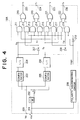
- Fig. 3 illustrates the detailed structure of the inverter switching circuit 17A which comprises an input terminal 170 connected to the carrier signal generator 6A, a peak detecting circuit 171 for detecting the peak of the signal supplied to the input terminal 170, a 1/2 divider 172 the polarity of the output signal from which is inverted in synchronization with the output from the peak detecting circuit 171, NOT circuit 173 connected to the 1/2 divider 172 and output terminals 174 to 177.
- Fig. 4 illustrates the detailed structure of the switching signal generating circuit 18A which comprises an input terminal 200 connected to the carrier signal generator 6A, an input terminal 201 connected to the reference voltage signal generating circuit 16, an absolute circuit 202, a comparator 203 constituted in such a manner that it transmits an output signal having a narrow width at an intersection between the last transition slope of the carrier signal V p and the reference voltage signal
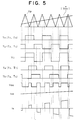
- carrier signal V p in the triangular form as shown in the uppermost portion of Fig. 5 is transmitted from the carrier signal generator 6A.
- ON/OFF signals T1 to T4 the duty ratio of each of which is 50 % are transmitted from the inverter switching circuit 17A due to the following operation: referring to Fig. 3, the carrier signal V p is supplied via the input terminal 170, signal synchronized with the peak of the carrier signal V p is input to the 1/2 divider 172 by the peak detecting circuit 171, signal T x shown in Fig.
- reference voltage signal V cc * which denotes the voltage to be transmitted from the cyclo-converter circuit 15, is transmitted from the reference voltage signal generating circuit 16 so as to be supplied to the switching signal generating circuit 18A together with the carrier signal V p .
- the switching signal generating circuit 18A receives the above-described signals V cc * and V p , it transmits the switching signals T5 to T8, the pulse width of each of which has been modulated, as follows: referring to Fig. 4, the reference voltage signal V cc * supplied through the input terminal 201 is converted into absolute signal
- is divided into two portions either of which is supplied to the comparator 203 so as to be subjected to a comparison with the last transition of the carrier signal V p supplied via the input terminal 200 and the other of which is supplied to the comparator 205 so as to be subjected to a comparison with the first transition of V p .
- the output from the comparator 203 is transmitted to the 1/2 divider 204 which then transmits a signal T a shown in Fig. 5.
- the output from the comparator 205 is transmitted to the 1/2 divider 206 which then transmits signal T b shown in Fig. 5.
- signal T a is supplied to the NOT circuit 207
- signal T c is transmitted.
- signal T b is supplied to the NOT circuit 208
- signal T d is transmitted. Then, the relationships among the signals T a to T d and the output voltage V cc from the cyclo-converter circuit 15 will be described.
- V cc V2.
- V cc - V2.
- V cc 0. Therefore, the output voltage V cc from the cyclo-converter circuit 15 is, as shown in Fig. 5, subjected to the PWM operation so as to be made positive voltage.
- the polarity discriminating circuit 209 transmits polarity signal V sgn of the reference voltage signal V cc *. Furthermore, the NOT circuit 210 transmits a signal obtained by inverting the sign of the polarity signal V sgn .
- the above-described signals and signals T a to T d are supplied to the OR circuits 219 to 222 via the AND circuits 211 to 218.
- the signals T a , T c , T d and T b are transmitted from the corresponding AND circuits 211, 214, 216 and 217.
- the output terminals 223 to 226 transmit the switching signal T5 to T8 which correspond to Equation (4).
- the switching signals T5 to T8 corresponding to Equation (6) are transmitted.
- Output current I cc from the cyclo-converter 15 is, as shown in Fig. 5, a continuous electric current which is determined by the filter circuit 4 and the load circuit 13.
- the electric current which passes through the cyclo-converter 15 repeats the following two modes due to the PWM operation performed by the switching element, that is, a mode in which it passes through the cyclo-converter 15 and another mode in which it circulates in the cyclo-converter 15:
- the input electric current I s received by the cyclo-converter 15 passes in only a period in which the voltage V cc is transmitted.
- the pulse width of V cc is controlled in such a manner that its center is made to be the zero point of the carrier signal V p .
- its width becomes the width between two peaks of V p when the pulse width becomes largest. Therefore, by setting the gain of the reference voltage generating circuit 16 in such a manner that the maximum absolute value
- the switching loss of the switching element of the inverter 14 relates to the electric current, which passes through the switching element, and the applied voltage. Therefore, when the level of the electric current is zero, no switching loss is generated. That is, the inverter 14 is able to be operated while preventing the switching loss.
- FIG. 6 is a block diagram which illustrates the third embodiment.
- reference numeral 4A represents a filter circuit
- 15A represents a cyclo-converter circuit
- 16A represents a reference voltage signal generating circuit.
- Reference numeral 18B represents a first switching signal generating circuit
- 30A represents a second switching signal generating circuit
- 13A represents a three-phase load circuit connected to the above-described DC-to-AC electric power converting apparatus.
- the other elements are the same as the elements according to the first embodiment.
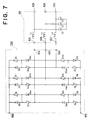
- Fig. 7 illustrates the detailed structure of the cyclo-converter circuit 15A and that of the filter circuit 4A.
- the cyclo-converter circuit 15A comprises input terminals 400 and 401 connected to the secondary coil terminals 23 and 24 of the transformer 2A, semiconductor switching devices S5 to S10 and S 5A to S 10A such as transistors and MOSFETs, diodes D5 to D10 and D 5A to D 10A connected to the above-described switching devices S5 to S10 and S 5A to S 10A in an inverted parallel manner and output terminals 402 and 404 connected to the filter circuit 4A.
- semiconductor switching devices S5 to S10 and S 5A to S 10A such as transistors and MOSFETs
- diodes D5 to D10 and D 5A to D 10A connected to the above-described switching devices S5 to S10 and S 5A to S 10A in an inverted parallel manner and output terminals 402 and 404 connected to the filter circuit 4A.
- the filter circuit 4A comprises input terminals 405 to 407 respectively connected to the output terminals 402 to 404 of the cyclo-converter circuit 15A, reactors L F and condensers C F and output terminals 408 to 410.
- Fig. 8 illustrates the detailed structure of the first switching signal generating circuit 18B which comprises input terminals 420 to 422 connected to the reference voltage signal generating circuit 16A, an input terminal 423 connected to the carrier signal generator 6A, comparators 424 to 426, NOT circuits 430 to 432, polarity discriminating circuits 433 to 435 and output terminals 436 to 444.
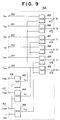
- Fig. 9 illustrates the detailed structure of the second switching signal generating circuit 30A which comprises input terminals 450 to 455 connected to the output terminals 436 to 441 of the first switching signal generating circuit 18B, input terminals 456 to 458 connected to the output terminals 442 to 444, an input terminal 459 connected to the inverter switching circuit 17, XOR (exclusive OR) circuits 462 to 470 and output terminals 471 to 476.
- XOR exclusive OR
- the operation of the second embodiment will be described with reference to Fig. 10.
- the triangle shape carrier signal V p shown in the uppermost portion of Fig. 10 is transmitted from the carrier signal generator 6A.
- the carrier signal V p is then supplied to the inverter switching circuit 17 so that the inverter switching circuit 17 transmits the ON/OFF signals T1 to T4.
- the four semiconductor switching devices S1 to S4 of the inverter circuit 14 are switched on/off in response to the ON/OFF signals T1 to T4.
- the secondary voltage V2 of the transformer 2A becomes rectangular waveform voltage the duty ratio of which is 50 % as shown in Fig. 10. Since the above-described operation is the same as that according to the first embodiment, the detailed description is omitted here.
- the operation of the four switching devices S5, S6, S 5A and S 6A included in the cyclo-converter circuit 15A for controlling the voltage of the phase u will be described with reference to Fig. 10.
- the u-phase reference voltage signal V ccu* supplied to the input terminal 420 of the first switching signal generating circuit 18B is, together with the carrier signal V p supplied to the input terminal 423, supplied to the comparator 424.
- the first switching signal T pu as shown in Fig. 10 is transmitted from the comparator 424.
- the signal T pu is supplied to the NOT circuit 430 so that the first switching signal T qu shown in Fig. 10 is transmitted.
- the operation of the second switching signal generating circuit 30A will be described.
- the u-phase voltage polarity signal V sgu transmitted from the first switching signal generating circuit 18B and the signal Tx, which is shown in Fig. 10, transmitted from the inverter switching circuit 17A are supplied to the XOR circuit 462 via the input terminals 456 and 459.
- the XOR circuit 462 transmits the signal Y u of a high level when the level of the polarity signal V sgu and that of the signal Tx are the same (that is, the polarity of the u-phase output voltage V ccu of the cyclo-converter 15A and that of the secondary voltage V2 of the transformer 2A are the same).
- the XOR circuit 462 transmits the Y u signal of a low level when the level of the polarity signal V sgn and that of the signal Tx are different from each other. Then, the switching signals T pu and T qu transmitted from the first switching signal generating circuit 18B are supplied via the input terminals 450 and 451 so as to be supplied, together with the signal Y u , to the XOR circuits 465 and 466. In response to this, the second switching signals T5 and T6 which correspond to the polarity of the secondary voltage V2 are transmitted from the XOR circuits 465 and 466 through the output terminals 471 and 472. As a result, the switching devices S5, S6, S 5A and S 6A are switched on/off.
- the waveform of the voltage V uo becomes as shown in Fig. 10, the waveform being formed by pulse-width modulating in such a manner that its basic wave component becomes V ccu* corresponding to the PWM signal T pu .
- the waveforms of the v-phase output voltage V vo and the w-phase output voltage V wo become those corresponding to the reference signals V ccv* and V ccw* , respectively before they are transmitted to the v-phase output terminal 403 and the w-phase output terminal 404, respectively.
- the high frequency components of the output voltages V uo , V vo and V wo are removed by the filter circuit 4A before they are transmitted to the output terminals 408 to 410 so as to be supplied to the load circuit 13A.
- the three-phase circuit has a plurality of arms through which the electric current circulates, it circulates through the v-phase arms (S7 and S 7A or S8 and S 8A ), the w-phase arms (S9 and S 9A or S10 and S 10A ) or both the above-described arms in a case of, for example, the u-phase electric current I ccu circulates.
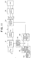
- Fig. 11 is a block diagram which illustrates the structure of the third embodiment, where reference numeral 6B represents a carrier signal generator for generating a sawtooth-shaped carrier signal, 17B represents an inverter switching circuit and 18C represents a switching signal generating circuit.
- the other structures are the same as those according to the second embodiment shown in Fig. 6.
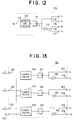
- Fig. 12 illustrates the detailed structure of the inverter switching circuit 17B which is structured in the same manner as the inverter switching circuit 17A according to the first and second embodiments except for the arrangement in which a detection circuit 178 is employed in place of the peak detection circuit 171, the detection circuit 178 according to this embodiment acting to generate a signal at the first transition edge of the input signal supplied to the input terminal 170.
- Fig. 13 illustrates the detailed structure of the switching signal generating circuit 18C which comprises the input terminals 420 to 422 connected to the reference signal generating circuit 16A, the input terminal 423 connected to the carrier signal generator 6B, comparators 433 to 435 arranged to transmit output signals each of which has a narrow width at the intersections between the last transition slope of the carrier signal V p and the reference voltage signals V ccu* , V ccv* and V ccw* , 1/2 dividers 427 to 429, NOT circuits 430 to 432 and the output terminals 471 to 476.
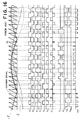
- the carrier signal V p formed into a sawtooth shape which is lowered to the right as shown in Fig. 14 is transmitted from the carrier signal generator 6B. Then, by supplying the carrier signal V p thus-transmitted to the inverter switching circuit 17B, an inverter ON/OFF signal T x (T1, T4) and T y (T2, T3) which synchronize with the first transition edge of V p is transmitted to the inverter circuit 14, causing the four switching elements S1 to S4 of the inverter circuit 14 to be switched on/off by corresponding signals. As a result, the secondary voltage V2 of the transformer 2A becomes, as shown in Fig.
- the reference voltage signal generating circuit 16A transmits the three-phase AC reference voltage signals V ccu* , V ccv* and V ccw* before they are, together with the above-described carrier signal V p , supplied to the switching signal generating circuit 18C.
- a narrow-width pulse is transmitted from the comparator 433 at the intersection between the first transition slope of the carrier signal V p and the reference voltage signal V ccu* before it is divided by the 1/2 divider 427.
- the switching signal T5 formed as shown in Fig. 14 is transmitted to the output terminal 471.
- the signal T6 obtained by inverting the signal T5 in the NOT circuit 430 is transmitted to the output terminal 472.
- the signals T7 and T8 which correspond to the phase v are transmitted to the output terminals 473 and 474 and the signals T9 and T10 corresponding to the phase w are transmitted to the output terminals 475 and 476.
- the signals T5, T7 and T9 respectively first-rise or trail in the same period of the carrier signal V p .
- the switching signals T5 to T10 respectively switch on/off the switching element pairs composed of the switching elements S5 - S 5A to S10 - S 10A of the cyclo-converter circuit 15A.
- the output voltage V uo formed by pulse-width-modulating V ccu* can be obtained at the u-phase output terminal 402 of the cyclo-converter circuit 15A, while the output voltage V vo formed by pulse-width modulating V ccv* can be obtained at the v-phase output terminal 403 of the same.
- the voltage V uv between the phases u and v becomes the difference between V uo and V vo .
- the third embodiment is enabled to have the cyclo-converter electric current passing mode and the circulating mode. Taking note of the electric current I uv which passes between the phase u and the phase v, the period in which the voltage is transmitted to V uv becomes the passing mode similarly to the first embodiment. Therefore, the waveform of the uv component in I s becomes as shown in Fig. 14.
- the cyclo-converter can be constituted as the mono-phase output similarly to the first embodiment.
Landscapes
- Engineering & Computer Science (AREA)
- Power Engineering (AREA)
- Inverter Devices (AREA)
- Ac-Ac Conversion (AREA)
Claims (6)
- Dispositif de conversion de puissance électrique courant continu en courant alternatif comprenant :
un circuit inverseur (14) ayant un certain nombre d'éléments de commutation et convertissant l'énergie électrique en courant continu en énergie électrique à courant alternatif ;
un transformateur (2A) relié audit circuit inverseur (14);
un circuit cyclo-convertisseur (15; 15A) pour convertir la fréquence de la sortie dudit transformateur (2A);
un générateur de signal de porteuse (6A; 6B) pour produire un signal de porteuse (Vp) d'une fréquence prédéterminée;
un circuit de commutation d'inverseur (17; 17A; 17B) pour commander l'opération de commutation de ladite pluralité d'éléments de commutation dudit circuit inverseur (14) en synchronisation avec ledit signal de porteuse (Vp);
un circuit de production de signal de tension de référence (16; 16A) pour produire un signal de tension de référence (Vcc*) pour la tension alternative à transmettre par le circuit cyclo-convertisseur (15; 15A), et
un circuit de production de signal de commutation (18A; 18B; 30A; 18C) pour commander le circuit cyclo-convertisseur (15; 15A) en réponse audit signal de tension de référence (Vcc*) produit par ledit circuit de production de signal de tension de référence (16; 16A) et le signal de porteuse (Vp) produit par ledit générateur de signal de porteuse (6A; 6B);
caractérisé en ce que
le circuit de commutation inverseur (17; 17A; 17B) commande l'opération de commutation de ladite pluralité d'éléments de commutation dudit circuit inverseur (14) en synchronisation avec des crêtes ou des transitions dudit signal de porteuse (Vp); et
le circuit de production du signal de commutation (18A; 18B; 30A; 18C) commande ledit circuit cyclo-convertisseur (15; 15A) de sorte qu'un signal de sortie (Vcc) est modulé en largeur d'impulsion ayant des parties dans lesquelles un courant électrique de sortie (Is) dudit circuit cyclo-convertisseur (15; 15A) circule dans ledit circuit cyclo-convertisseur (15; 15A) synchronisé avec lesdites crêtes ou transitions du signal de porteuse (Vp). - Dispositif selon la revendication 1, dans lequel le circuit de commutation d'inverseur précité (17; 17A; 17B) met en service/hors service la pluralité précitée d'éléments de commutation précités du circuit inverseur précité (14) dans une période dans laquelle un courant électrique de sortie du circuit cyclo-convertisseur précité (15; 15A) circule dans ledit circuit cyclo-convertisseur.
- Dispositif selon la revendication 1, dans lequel le circuit de commutation d'inverseur précité (17; 17A; 17B) transmet un signal de commande, dont le cycle de travail est d'environ 50%, au circuit inverseur précité (14).
- Dispositif selon la revendication 1, dans lequel le circuit cyclo-convertisseur précité (15; 15A) comprend un certain nombre d'éléments de commutation et transmet la puissance alternative qui a été soumise à une modulation de largeur d'impulsion.
- Dispositif selon la revendication 1, dans lequel le circuit cyclo-convertisseur précité (15; 15A) transmet la puissance alternative multiphasée.
- Dispositif selon la revendication 1, comprenant de plus un circuit de filtrage (4) pour retirer la composante haute fréquence du signal de sortie (Vcc) du circuit cyclo-convertisseur précité (15).
Applications Claiming Priority (2)
| Application Number | Priority Date | Filing Date | Title |
|---|---|---|---|
| JP2240951A JP2539538B2 (ja) | 1990-09-10 | 1990-09-10 | 直流交流電力変換装置 |
| JP240951/90 | 1990-09-10 |
Publications (3)
| Publication Number | Publication Date |
|---|---|
| EP0475345A2 EP0475345A2 (fr) | 1992-03-18 |
| EP0475345A3 EP0475345A3 (en) | 1992-05-27 |
| EP0475345B1 true EP0475345B1 (fr) | 1995-04-05 |
Family
ID=17067083
Family Applications (1)
| Application Number | Title | Priority Date | Filing Date |
|---|---|---|---|
| EP91115268A Expired - Lifetime EP0475345B1 (fr) | 1990-09-10 | 1991-09-10 | Dispositif convertisseur de puissance courant continu/courant alternatif |
Country Status (6)
| Country | Link |
|---|---|
| US (1) | US5189603A (fr) |
| EP (1) | EP0475345B1 (fr) |
| JP (1) | JP2539538B2 (fr) |
| KR (1) | KR960003407B1 (fr) |
| CA (1) | CA2051017C (fr) |
| DE (1) | DE69108650T2 (fr) |
Families Citing this family (30)
| Publication number | Priority date | Publication date | Assignee | Title |
|---|---|---|---|---|
| EP1249928A1 (fr) * | 2001-04-10 | 2002-10-16 | Siemens Aktiengesellschaft | Procédé et convertisseur de tension pour transformer une tension d'entrée courant continu dans une tension de sortie courant alternatif avec une fréquence proche de la fréquence du réseau électrique |
| US7102331B2 (en) * | 2003-01-17 | 2006-09-05 | Black & Decker Inc. | Generator with dual cycloconverter for 120/240 VAC operation |
| JP4318174B2 (ja) * | 2003-12-11 | 2009-08-19 | 本田技研工業株式会社 | Dc−dcコンバータ |
| JP5034229B2 (ja) * | 2005-12-14 | 2012-09-26 | 日本精工株式会社 | 車載用モータ制御装置、これを使用した電動パワーステアリング装置及び電動ブレーキ装置 |
| US7599196B2 (en) * | 2006-06-06 | 2009-10-06 | Ideal Power Converters, Inc. | Universal power converter |
| US8514601B2 (en) | 2009-08-17 | 2013-08-20 | Ideal Power Converters, Inc. | Power conversion with added pseudo-phase |
| US7599204B2 (en) * | 2006-08-29 | 2009-10-06 | Gm Global Technology Operations, Inc. | Control scheme providing a freewheeling period in a cyclo-converter and a high frequency inverter |
| US7483282B2 (en) * | 2006-08-29 | 2009-01-27 | Gm Global Technology Operations, Inc. | PWM method for cycloconverter |
| US20080205109A1 (en) * | 2007-02-26 | 2008-08-28 | Lear Corporation | Energy distribution system for vehicle |
| US20100244773A1 (en) * | 2009-03-27 | 2010-09-30 | Gm Global Technology Operations, Inc. | Unity power factor isolated single phase matrix converter battery charger |
| KR20120130158A (ko) | 2009-06-29 | 2012-11-29 | 아이디얼 파워 컨버터스, 인코포레이티드 | 에너지 전송 리액턴스를 단락시키는 크로바 스위치를 이용한 전력 전송 장치, 방법, 및 시스템 |
| US20110006720A1 (en) * | 2009-07-08 | 2011-01-13 | Innosave Ltd. | Method and apparatus for ac motor control |
| US8207699B2 (en) * | 2009-07-08 | 2012-06-26 | Innosave Ltd. | Method and apparatus for AC motor control |
| US8466658B2 (en) * | 2009-08-05 | 2013-06-18 | GM Global Technology Operations LLC | Systems and methods for bi-directional energy delivery with galvanic isolation |
| US8559193B2 (en) * | 2010-01-22 | 2013-10-15 | The Board Of Trustees Of The University Of Illinois | Zero-voltage-switching scheme for high-frequency converter |
| US8410635B2 (en) * | 2010-03-16 | 2013-04-02 | GM Global Technology Operations LLC | Systems and methods for deactivating a matrix converter |
| US8462528B2 (en) * | 2010-07-19 | 2013-06-11 | GM Global Technology Operations LLC | Systems and methods for reducing transient voltage spikes in matrix converters |
| US8599577B2 (en) | 2010-11-08 | 2013-12-03 | GM Global Technology Operations LLC | Systems and methods for reducing harmonic distortion in electrical converters |
| US8467197B2 (en) | 2010-11-08 | 2013-06-18 | GM Global Technology Operations LLC | Systems and methods for compensating for electrical converter nonlinearities |
| US8587962B2 (en) | 2010-11-08 | 2013-11-19 | GM Global Technology Operations LLC | Compensation for electrical converter nonlinearities |
| US8614564B2 (en) | 2010-11-18 | 2013-12-24 | GM Global Technology Operations LLS | Systems and methods for providing power to a load based upon a control strategy |
| WO2012075172A2 (fr) | 2010-11-30 | 2012-06-07 | Ideal Power Converters Inc. | Systèmes, procédés, et dispositifs de réseaux photovoltaïques, et diagnostic et surveillance améliorés |
| US8531858B2 (en) | 2011-02-18 | 2013-09-10 | Ideal Power, Inc. | Power conversion with current sensing coupled through saturating element |
| US8860379B2 (en) | 2011-04-20 | 2014-10-14 | GM Global Technology Operations LLC | Discharging a DC bus capacitor of an electrical converter system |
| US8829858B2 (en) | 2011-05-31 | 2014-09-09 | GM Global Technology Operations LLC | Systems and methods for initializing a charging system |
| US8878495B2 (en) | 2011-08-31 | 2014-11-04 | GM Global Technology Operations LLC | Systems and methods for providing power to a load based upon a control strategy |
| US20140268927A1 (en) * | 2013-03-14 | 2014-09-18 | Vanner, Inc. | Voltage converter systems |
| US9770991B2 (en) | 2013-05-31 | 2017-09-26 | GM Global Technology Operations LLC | Systems and methods for initializing a charging system |
| JP2016226162A (ja) * | 2015-05-29 | 2016-12-28 | 株式会社豊田中央研究所 | 絶縁型電力変換装置 |
| CN107294414B (zh) * | 2016-04-08 | 2020-09-18 | 松下知识产权经营株式会社 | 电力变换装置 |
Family Cites Families (14)
| Publication number | Priority date | Publication date | Assignee | Title |
|---|---|---|---|---|
| US3487289A (en) * | 1968-04-16 | 1969-12-30 | Gen Electric | Multipurpose power converter circuits |
| US3742336A (en) * | 1971-11-24 | 1973-06-26 | Gen Electric | Versatile cycloinverter power converter circuits |
| US4240135A (en) * | 1979-05-29 | 1980-12-16 | Bell Telephone Laboratories, Incorporated | Regulated cycloconverter circuit |
| US4479175A (en) * | 1982-08-13 | 1984-10-23 | Honeywell Inc. | Phase modulated switchmode power amplifier and waveform generator |
| JPS59178975A (ja) * | 1983-03-29 | 1984-10-11 | Mitsubishi Electric Corp | インバ−タ |
| US4556937A (en) * | 1983-10-05 | 1985-12-03 | Canadian Patents And Development Limited | DC-AC Power converter including two high frequency resonant link converters |
| JPS6176069A (ja) * | 1984-09-20 | 1986-04-18 | Mitsubishi Electric Corp | コンバ−タ装置 |
| JPS61173636A (ja) * | 1984-12-18 | 1986-08-05 | 三菱電機株式会社 | 電源装置 |
| JPS6268068A (ja) * | 1985-09-20 | 1987-03-27 | Mitsubishi Electric Corp | 電力変換装置 |
| EP0293869B1 (fr) * | 1987-06-05 | 1993-09-01 | Hitachi, Ltd. | Dispositif de conversion de puissance |
| JPH0746906B2 (ja) * | 1987-08-17 | 1995-05-17 | 三菱電機株式会社 | 電圧変換装置 |
| DE3877679T2 (de) * | 1987-09-30 | 1993-08-05 | Hitachi Ltd | Leistungsumwandlungseinrichtung. |
| JPH0755056B2 (ja) * | 1988-05-25 | 1995-06-07 | 山洋電気株式会社 | インバータ装置 |
| JPH0783615B2 (ja) * | 1988-11-28 | 1995-09-06 | 三菱電機株式会社 | 三相変換器 |
-
1990
- 1990-09-10 JP JP2240951A patent/JP2539538B2/ja not_active Expired - Fee Related
-
1991
- 1991-09-07 KR KR1019910015640A patent/KR960003407B1/ko not_active Expired - Fee Related
- 1991-09-09 US US07/756,426 patent/US5189603A/en not_active Expired - Fee Related
- 1991-09-09 CA CA002051017A patent/CA2051017C/fr not_active Expired - Fee Related
- 1991-09-10 DE DE69108650T patent/DE69108650T2/de not_active Expired - Fee Related
- 1991-09-10 EP EP91115268A patent/EP0475345B1/fr not_active Expired - Lifetime
Also Published As
| Publication number | Publication date |
|---|---|
| KR920007312A (ko) | 1992-04-28 |
| CA2051017C (fr) | 1997-11-25 |
| JP2539538B2 (ja) | 1996-10-02 |
| CA2051017A1 (fr) | 1992-03-11 |
| DE69108650D1 (de) | 1995-05-11 |
| JPH04121067A (ja) | 1992-04-22 |
| US5189603A (en) | 1993-02-23 |
| DE69108650T2 (de) | 1995-09-28 |
| EP0475345A2 (fr) | 1992-03-18 |
| EP0475345A3 (en) | 1992-05-27 |
| KR960003407B1 (ko) | 1996-03-09 |
Similar Documents
| Publication | Publication Date | Title |
|---|---|---|
| EP0475345B1 (fr) | Dispositif convertisseur de puissance courant continu/courant alternatif | |
| US5159539A (en) | High frequency DC/AC power converting apparatus | |
| Kawabata et al. | High frequency link DC/AC converter with PWM cycloconverter | |
| US6166513A (en) | Four-quadrant AC-AC drive and method | |
| US4354223A (en) | Step-up/step down chopper | |
| EP0152796B1 (fr) | Dispositif de commande pour convertisseur de puissance | |
| EP0642212A1 (fr) | Convertisseur à trois niveaux avec un appareil pour l'égalisation de la composante de courant continu | |
| US20010038541A1 (en) | Drive and power supply with phase shifted carriers | |
| EP0293869B1 (fr) | Dispositif de conversion de puissance | |
| JPH04197078A (ja) | 電力変換装置 | |
| TW353244B (en) | Power converter and power converting method | |
| EP0481456A2 (fr) | Dispositif de conversion de puissance | |
| JPH09131075A (ja) | インバータ装置 | |
| CN100385783C (zh) | 供电电源 | |
| JP3337041B2 (ja) | 単相3線式インバータ装置の制御方法 | |
| KR20230003888A (ko) | 모터 구동 시스템을 이용한 충전 시스템 및 방법 | |
| EP0503631B1 (fr) | Dispositif de conversion de puissance à circuit intermédiaire à haute fréquence | |
| CN114499191A (zh) | 功率变换器 | |
| JP2582920B2 (ja) | 直流一交流電力変換装置 | |
| JP3080542B2 (ja) | 高周波トランス結合による搬送波周波数変調のインバータ・システム | |
| JPH0880060A (ja) | 単相インバータ装置 | |
| JPH10191641A (ja) | 無停電電源装置 | |
| JP3134301B2 (ja) | 交流電源装置 | |
| JP3640260B2 (ja) | Ac/acコンバータ | |
| JP2005012857A (ja) | 電力変換装置 |
Legal Events
| Date | Code | Title | Description |
|---|---|---|---|
| PUAI | Public reference made under article 153(3) epc to a published international application that has entered the european phase |
Free format text: ORIGINAL CODE: 0009012 |
|
| AK | Designated contracting states |
Kind code of ref document: A2 Designated state(s): DE FR GB |
|
| PUAL | Search report despatched |
Free format text: ORIGINAL CODE: 0009013 |
|
| AK | Designated contracting states |
Kind code of ref document: A3 Designated state(s): DE FR GB |
|
| 17P | Request for examination filed |
Effective date: 19920804 |
|
| 17Q | First examination report despatched |
Effective date: 19940301 |
|
| GRAA | (expected) grant |
Free format text: ORIGINAL CODE: 0009210 |
|
| AK | Designated contracting states |
Kind code of ref document: B1 Designated state(s): DE FR GB |
|
| REF | Corresponds to: |
Ref document number: 69108650 Country of ref document: DE Date of ref document: 19950511 |
|
| REG | Reference to a national code |
Ref country code: GB Ref legal event code: 727 |
|
| ET | Fr: translation filed | ||
| REG | Reference to a national code |
Ref country code: GB Ref legal event code: 727A |
|
| REG | Reference to a national code |
Ref country code: GB Ref legal event code: 727B |
|
| PLBE | No opposition filed within time limit |
Free format text: ORIGINAL CODE: 0009261 |
|
| STAA | Information on the status of an ep patent application or granted ep patent |
Free format text: STATUS: NO OPPOSITION FILED WITHIN TIME LIMIT |
|
| 26N | No opposition filed | ||
| REG | Reference to a national code |
Ref country code: GB Ref legal event code: SP |
|
| REG | Reference to a national code |
Ref country code: GB Ref legal event code: IF02 |
|
| PGFP | Annual fee paid to national office [announced via postgrant information from national office to epo] |
Ref country code: DE Payment date: 20040902 Year of fee payment: 14 |
|
| PGFP | Annual fee paid to national office [announced via postgrant information from national office to epo] |
Ref country code: GB Payment date: 20040908 Year of fee payment: 14 Ref country code: FR Payment date: 20040908 Year of fee payment: 14 |
|
| PG25 | Lapsed in a contracting state [announced via postgrant information from national office to epo] |
Ref country code: GB Free format text: LAPSE BECAUSE OF NON-PAYMENT OF DUE FEES Effective date: 20050910 |
|
| PG25 | Lapsed in a contracting state [announced via postgrant information from national office to epo] |
Ref country code: DE Free format text: LAPSE BECAUSE OF NON-PAYMENT OF DUE FEES Effective date: 20060401 |
|
| GBPC | Gb: european patent ceased through non-payment of renewal fee |
Effective date: 20050910 |
|
| PG25 | Lapsed in a contracting state [announced via postgrant information from national office to epo] |
Ref country code: FR Free format text: LAPSE BECAUSE OF NON-PAYMENT OF DUE FEES Effective date: 20060531 |
|
| REG | Reference to a national code |
Ref country code: FR Ref legal event code: ST Effective date: 20060531 |