EP0475372B1 - Oberflächenemittierender Halbleiterlaser - Google Patents
Oberflächenemittierender Halbleiterlaser Download PDFInfo
- Publication number
- EP0475372B1 EP0475372B1 EP91115317A EP91115317A EP0475372B1 EP 0475372 B1 EP0475372 B1 EP 0475372B1 EP 91115317 A EP91115317 A EP 91115317A EP 91115317 A EP91115317 A EP 91115317A EP 0475372 B1 EP0475372 B1 EP 0475372B1
- Authority
- EP
- European Patent Office
- Prior art keywords
- layer
- semiconductor laser
- column
- semiconductor
- laser
- Prior art date
- Legal status (The legal status is an assumption and is not a legal conclusion. Google has not performed a legal analysis and makes no representation as to the accuracy of the status listed.)
- Expired - Lifetime
Links
- 239000004065 semiconductor Substances 0.000 title claims description 129
- 238000000926 separation method Methods 0.000 claims description 27
- 239000000758 substrate Substances 0.000 claims description 26
- 230000003287 optical effect Effects 0.000 claims description 20
- 238000005253 cladding Methods 0.000 claims description 19
- 150000001875 compounds Chemical class 0.000 claims description 18
- 239000012071 phase Substances 0.000 claims description 14
- 230000001360 synchronised effect Effects 0.000 claims description 9
- 230000004888 barrier function Effects 0.000 claims description 6
- 238000002310 reflectometry Methods 0.000 claims description 5
- 229910052793 cadmium Inorganic materials 0.000 claims description 2
- 229910052753 mercury Inorganic materials 0.000 claims description 2
- 229910052711 selenium Inorganic materials 0.000 claims description 2
- 229910052717 sulfur Inorganic materials 0.000 claims description 2
- 229910052714 tellurium Inorganic materials 0.000 claims description 2
- 229910052725 zinc Inorganic materials 0.000 claims description 2
- 239000012808 vapor phase Substances 0.000 claims 1
- 238000000034 method Methods 0.000 description 28
- VYPSYNLAJGMNEJ-UHFFFAOYSA-N Silicium dioxide Chemical compound O=[Si]=O VYPSYNLAJGMNEJ-UHFFFAOYSA-N 0.000 description 26
- 230000008569 process Effects 0.000 description 22
- 229910052681 coesite Inorganic materials 0.000 description 13
- 229910052906 cristobalite Inorganic materials 0.000 description 13
- 239000000377 silicon dioxide Substances 0.000 description 13
- 235000012239 silicon dioxide Nutrition 0.000 description 13
- 229910052682 stishovite Inorganic materials 0.000 description 13
- 229910052905 tridymite Inorganic materials 0.000 description 13
- 229910001218 Gallium arsenide Inorganic materials 0.000 description 11
- 239000000463 material Substances 0.000 description 11
- 238000005530 etching Methods 0.000 description 9
- 229910000980 Aluminium gallium arsenide Inorganic materials 0.000 description 6
- 238000002488 metal-organic chemical vapour deposition Methods 0.000 description 6
- 238000001020 plasma etching Methods 0.000 description 6
- 239000007789 gas Substances 0.000 description 5
- XKRFYHLGVUSROY-UHFFFAOYSA-N Argon Chemical compound [Ar] XKRFYHLGVUSROY-UHFFFAOYSA-N 0.000 description 4
- 239000002019 doping agent Substances 0.000 description 4
- 230000005855 radiation Effects 0.000 description 4
- 238000010884 ion-beam technique Methods 0.000 description 3
- 238000004943 liquid phase epitaxy Methods 0.000 description 3
- 239000000203 mixture Substances 0.000 description 3
- 238000000927 vapour-phase epitaxy Methods 0.000 description 3
- ZAMOUSCENKQFHK-UHFFFAOYSA-N Chlorine atom Chemical compound [Cl] ZAMOUSCENKQFHK-UHFFFAOYSA-N 0.000 description 2
- 229910052786 argon Inorganic materials 0.000 description 2
- 230000008901 benefit Effects 0.000 description 2
- 230000000903 blocking effect Effects 0.000 description 2
- 239000000969 carrier Substances 0.000 description 2
- 239000000460 chlorine Substances 0.000 description 2
- 229910052801 chlorine Inorganic materials 0.000 description 2
- 230000003247 decreasing effect Effects 0.000 description 2
- HQWPLXHWEZZGKY-UHFFFAOYSA-N diethylzinc Chemical compound CC[Zn]CC HQWPLXHWEZZGKY-UHFFFAOYSA-N 0.000 description 2
- 238000009826 distribution Methods 0.000 description 2
- 238000001312 dry etching Methods 0.000 description 2
- 238000000313 electron-beam-induced deposition Methods 0.000 description 2
- 238000002347 injection Methods 0.000 description 2
- 239000007924 injection Substances 0.000 description 2
- 230000031700 light absorption Effects 0.000 description 2
- 229910052751 metal Inorganic materials 0.000 description 2
- 239000002184 metal Substances 0.000 description 2
- 150000002739 metals Chemical class 0.000 description 2
- 230000009467 reduction Effects 0.000 description 2
- 238000002230 thermal chemical vapour deposition Methods 0.000 description 2
- JLTRXTDYQLMHGR-UHFFFAOYSA-N trimethylaluminium Chemical compound C[Al](C)C JLTRXTDYQLMHGR-UHFFFAOYSA-N 0.000 description 2
- XCZXGTMEAKBVPV-UHFFFAOYSA-N trimethylgallium Chemical compound C[Ga](C)C XCZXGTMEAKBVPV-UHFFFAOYSA-N 0.000 description 2
- 229910000530 Gallium indium arsenide Inorganic materials 0.000 description 1
- 229910004298 SiO 2 Inorganic materials 0.000 description 1
- 238000010521 absorption reaction Methods 0.000 description 1
- RBFQJDQYXXHULB-UHFFFAOYSA-N arsane Chemical compound [AsH3] RBFQJDQYXXHULB-UHFFFAOYSA-N 0.000 description 1
- 229910000070 arsenic hydride Inorganic materials 0.000 description 1
- 230000008859 change Effects 0.000 description 1
- 230000007423 decrease Effects 0.000 description 1
- 238000000151 deposition Methods 0.000 description 1
- 230000008021 deposition Effects 0.000 description 1
- 230000006872 improvement Effects 0.000 description 1
- 239000011810 insulating material Substances 0.000 description 1
- 150000002500 ions Chemical class 0.000 description 1
- 238000005304 joining Methods 0.000 description 1
- 230000004048 modification Effects 0.000 description 1
- 238000012986 modification Methods 0.000 description 1
- 229910052760 oxygen Inorganic materials 0.000 description 1
- 229920002120 photoresistant polymer Polymers 0.000 description 1
- SBIBMFFZSBJNJF-UHFFFAOYSA-N selenium;zinc Chemical compound [Se]=[Zn] SBIBMFFZSBJNJF-UHFFFAOYSA-N 0.000 description 1
- 239000007787 solid Substances 0.000 description 1
- 239000012780 transparent material Substances 0.000 description 1
- 238000001039 wet etching Methods 0.000 description 1
- 239000011701 zinc Substances 0.000 description 1
Images


Classifications
-
- H—ELECTRICITY
- H01—ELECTRIC ELEMENTS
- H01S—DEVICES USING THE PROCESS OF LIGHT AMPLIFICATION BY STIMULATED EMISSION OF RADIATION [LASER] TO AMPLIFY OR GENERATE LIGHT; DEVICES USING STIMULATED EMISSION OF ELECTROMAGNETIC RADIATION IN WAVE RANGES OTHER THAN OPTICAL
- H01S5/00—Semiconductor lasers
- H01S5/30—Structure or shape of the active region; Materials used for the active region
- H01S5/32—Structure or shape of the active region; Materials used for the active region comprising PN junctions, e.g. hetero- or double- heterostructures
-
- H—ELECTRICITY
- H01—ELECTRIC ELEMENTS
- H01S—DEVICES USING THE PROCESS OF LIGHT AMPLIFICATION BY STIMULATED EMISSION OF RADIATION [LASER] TO AMPLIFY OR GENERATE LIGHT; DEVICES USING STIMULATED EMISSION OF ELECTROMAGNETIC RADIATION IN WAVE RANGES OTHER THAN OPTICAL
- H01S5/00—Semiconductor lasers
- H01S5/10—Construction or shape of the optical resonator, e.g. extended or external cavity, coupled cavities, bent-guide, varying width, thickness or composition of the active region
- H01S5/18—Surface-emitting [SE] lasers, e.g. having both horizontal and vertical cavities
- H01S5/183—Surface-emitting [SE] lasers, e.g. having both horizontal and vertical cavities having only vertical cavities, e.g. vertical cavity surface-emitting lasers [VCSEL]
- H01S5/18308—Surface-emitting [SE] lasers, e.g. having both horizontal and vertical cavities having only vertical cavities, e.g. vertical cavity surface-emitting lasers [VCSEL] having a special structure for lateral current or light confinement
- H01S5/18338—Non-circular shape of the structure
-
- H—ELECTRICITY
- H01—ELECTRIC ELEMENTS
- H01S—DEVICES USING THE PROCESS OF LIGHT AMPLIFICATION BY STIMULATED EMISSION OF RADIATION [LASER] TO AMPLIFY OR GENERATE LIGHT; DEVICES USING STIMULATED EMISSION OF ELECTROMAGNETIC RADIATION IN WAVE RANGES OTHER THAN OPTICAL
- H01S5/00—Semiconductor lasers
- H01S5/40—Arrangement of two or more semiconductor lasers, not provided for in groups H01S5/02 - H01S5/30
- H01S5/42—Arrays of surface emitting lasers
- H01S5/423—Arrays of surface emitting lasers having a vertical cavity
-
- H—ELECTRICITY
- H10—SEMICONDUCTOR DEVICES; ELECTRIC SOLID-STATE DEVICES NOT OTHERWISE PROVIDED FOR
- H10H—INORGANIC LIGHT-EMITTING SEMICONDUCTOR DEVICES HAVING POTENTIAL BARRIERS
- H10H20/00—Individual inorganic light-emitting semiconductor devices having potential barriers, e.g. light-emitting diodes [LED]
- H10H20/01—Manufacture or treatment
- H10H20/011—Manufacture or treatment of bodies, e.g. forming semiconductor layers
- H10H20/013—Manufacture or treatment of bodies, e.g. forming semiconductor layers having light-emitting regions comprising only Group III-V materials
-
- H—ELECTRICITY
- H01—ELECTRIC ELEMENTS
- H01S—DEVICES USING THE PROCESS OF LIGHT AMPLIFICATION BY STIMULATED EMISSION OF RADIATION [LASER] TO AMPLIFY OR GENERATE LIGHT; DEVICES USING STIMULATED EMISSION OF ELECTROMAGNETIC RADIATION IN WAVE RANGES OTHER THAN OPTICAL
- H01S2301/00—Functional characteristics
- H01S2301/16—Semiconductor lasers with special structural design to influence the modes, e.g. specific multimode
- H01S2301/166—Single transverse or lateral mode
-
- H—ELECTRICITY
- H01—ELECTRIC ELEMENTS
- H01S—DEVICES USING THE PROCESS OF LIGHT AMPLIFICATION BY STIMULATED EMISSION OF RADIATION [LASER] TO AMPLIFY OR GENERATE LIGHT; DEVICES USING STIMULATED EMISSION OF ELECTROMAGNETIC RADIATION IN WAVE RANGES OTHER THAN OPTICAL
- H01S5/00—Semiconductor lasers
- H01S5/10—Construction or shape of the optical resonator, e.g. extended or external cavity, coupled cavities, bent-guide, varying width, thickness or composition of the active region
- H01S5/18—Surface-emitting [SE] lasers, e.g. having both horizontal and vertical cavities
- H01S5/183—Surface-emitting [SE] lasers, e.g. having both horizontal and vertical cavities having only vertical cavities, e.g. vertical cavity surface-emitting lasers [VCSEL]
- H01S5/18308—Surface-emitting [SE] lasers, e.g. having both horizontal and vertical cavities having only vertical cavities, e.g. vertical cavity surface-emitting lasers [VCSEL] having a special structure for lateral current or light confinement
-
- H—ELECTRICITY
- H01—ELECTRIC ELEMENTS
- H01S—DEVICES USING THE PROCESS OF LIGHT AMPLIFICATION BY STIMULATED EMISSION OF RADIATION [LASER] TO AMPLIFY OR GENERATE LIGHT; DEVICES USING STIMULATED EMISSION OF ELECTROMAGNETIC RADIATION IN WAVE RANGES OTHER THAN OPTICAL
- H01S5/00—Semiconductor lasers
- H01S5/10—Construction or shape of the optical resonator, e.g. extended or external cavity, coupled cavities, bent-guide, varying width, thickness or composition of the active region
- H01S5/18—Surface-emitting [SE] lasers, e.g. having both horizontal and vertical cavities
- H01S5/183—Surface-emitting [SE] lasers, e.g. having both horizontal and vertical cavities having only vertical cavities, e.g. vertical cavity surface-emitting lasers [VCSEL]
- H01S5/18361—Structure of the reflectors, e.g. hybrid mirrors
- H01S5/18369—Structure of the reflectors, e.g. hybrid mirrors based on dielectric materials
-
- H—ELECTRICITY
- H01—ELECTRIC ELEMENTS
- H01S—DEVICES USING THE PROCESS OF LIGHT AMPLIFICATION BY STIMULATED EMISSION OF RADIATION [LASER] TO AMPLIFY OR GENERATE LIGHT; DEVICES USING STIMULATED EMISSION OF ELECTROMAGNETIC RADIATION IN WAVE RANGES OTHER THAN OPTICAL
- H01S5/00—Semiconductor lasers
- H01S5/10—Construction or shape of the optical resonator, e.g. extended or external cavity, coupled cavities, bent-guide, varying width, thickness or composition of the active region
- H01S5/18—Surface-emitting [SE] lasers, e.g. having both horizontal and vertical cavities
- H01S5/183—Surface-emitting [SE] lasers, e.g. having both horizontal and vertical cavities having only vertical cavities, e.g. vertical cavity surface-emitting lasers [VCSEL]
- H01S5/18386—Details of the emission surface for influencing the near- or far-field, e.g. a grating on the surface
- H01S5/18394—Apertures, e.g. defined by the shape of the upper electrode
-
- H—ELECTRICITY
- H01—ELECTRIC ELEMENTS
- H01S—DEVICES USING THE PROCESS OF LIGHT AMPLIFICATION BY STIMULATED EMISSION OF RADIATION [LASER] TO AMPLIFY OR GENERATE LIGHT; DEVICES USING STIMULATED EMISSION OF ELECTROMAGNETIC RADIATION IN WAVE RANGES OTHER THAN OPTICAL
- H01S5/00—Semiconductor lasers
- H01S5/20—Structure or shape of the semiconductor body to guide the optical wave ; Confining structures perpendicular to the optical axis, e.g. index or gain guiding, stripe geometry, broad area lasers, gain tailoring, transverse or lateral reflectors, special cladding structures, MQW barrier reflection layers
- H01S5/22—Structure or shape of the semiconductor body to guide the optical wave ; Confining structures perpendicular to the optical axis, e.g. index or gain guiding, stripe geometry, broad area lasers, gain tailoring, transverse or lateral reflectors, special cladding structures, MQW barrier reflection layers having a ridge or stripe structure
- H01S5/2205—Structure or shape of the semiconductor body to guide the optical wave ; Confining structures perpendicular to the optical axis, e.g. index or gain guiding, stripe geometry, broad area lasers, gain tailoring, transverse or lateral reflectors, special cladding structures, MQW barrier reflection layers having a ridge or stripe structure comprising special burying or current confinement layers
- H01S5/2211—Structure or shape of the semiconductor body to guide the optical wave ; Confining structures perpendicular to the optical axis, e.g. index or gain guiding, stripe geometry, broad area lasers, gain tailoring, transverse or lateral reflectors, special cladding structures, MQW barrier reflection layers having a ridge or stripe structure comprising special burying or current confinement layers based on II-VI materials
-
- H—ELECTRICITY
- H01—ELECTRIC ELEMENTS
- H01S—DEVICES USING THE PROCESS OF LIGHT AMPLIFICATION BY STIMULATED EMISSION OF RADIATION [LASER] TO AMPLIFY OR GENERATE LIGHT; DEVICES USING STIMULATED EMISSION OF ELECTROMAGNETIC RADIATION IN WAVE RANGES OTHER THAN OPTICAL
- H01S5/00—Semiconductor lasers
- H01S5/20—Structure or shape of the semiconductor body to guide the optical wave ; Confining structures perpendicular to the optical axis, e.g. index or gain guiding, stripe geometry, broad area lasers, gain tailoring, transverse or lateral reflectors, special cladding structures, MQW barrier reflection layers
- H01S5/22—Structure or shape of the semiconductor body to guide the optical wave ; Confining structures perpendicular to the optical axis, e.g. index or gain guiding, stripe geometry, broad area lasers, gain tailoring, transverse or lateral reflectors, special cladding structures, MQW barrier reflection layers having a ridge or stripe structure
- H01S5/2205—Structure or shape of the semiconductor body to guide the optical wave ; Confining structures perpendicular to the optical axis, e.g. index or gain guiding, stripe geometry, broad area lasers, gain tailoring, transverse or lateral reflectors, special cladding structures, MQW barrier reflection layers having a ridge or stripe structure comprising special burying or current confinement layers
- H01S5/2222—Structure or shape of the semiconductor body to guide the optical wave ; Confining structures perpendicular to the optical axis, e.g. index or gain guiding, stripe geometry, broad area lasers, gain tailoring, transverse or lateral reflectors, special cladding structures, MQW barrier reflection layers having a ridge or stripe structure comprising special burying or current confinement layers having special electric properties
- H01S5/2224—Structure or shape of the semiconductor body to guide the optical wave ; Confining structures perpendicular to the optical axis, e.g. index or gain guiding, stripe geometry, broad area lasers, gain tailoring, transverse or lateral reflectors, special cladding structures, MQW barrier reflection layers having a ridge or stripe structure comprising special burying or current confinement layers having special electric properties semi-insulating semiconductors
-
- H—ELECTRICITY
- H01—ELECTRIC ELEMENTS
- H01S—DEVICES USING THE PROCESS OF LIGHT AMPLIFICATION BY STIMULATED EMISSION OF RADIATION [LASER] TO AMPLIFY OR GENERATE LIGHT; DEVICES USING STIMULATED EMISSION OF ELECTROMAGNETIC RADIATION IN WAVE RANGES OTHER THAN OPTICAL
- H01S5/00—Semiconductor lasers
- H01S5/40—Arrangement of two or more semiconductor lasers, not provided for in groups H01S5/02 - H01S5/30
- H01S5/4025—Array arrangements, e.g. constituted by discrete laser diodes or laser bar
- H01S5/4031—Edge-emitting structures
- H01S5/4068—Edge-emitting structures with lateral coupling by axially offset or by merging waveguides, e.g. Y-couplers
Definitions
- the present invention relates to a surface emission type semiconductor laser adapted to emit a laser beam in a direction perpendicular to the substrate thereof.
- a surface emission type laser including a resonator disposed in a direction perpendicular to the substrate thereof is disclosed in Lectures of the 50-th Meeting of Applied Physics in Japan (1989), Vol. 3, p. 909, 29a-ZG-7.
- Fig. 12 there is first provided an n-type GaAs substrate 602 on which an n-type AlGaAs/AlAs multi-layer film 603, an n-type AlGaAs cladding layer 604, a p-type GaAs active layer 605 and a p-type AlGaAs cladding layer 606 are sequentially grown and formed.
- the multi-layered structure is then etched while leaving a column-like part at the top thereof.
- Each of the left column-like part is enclosed by a buried layer which is formed by sequentially growing a p-type layer 607, n-type layer 608, p-type layer 609 and p-type layer 610 all of which are of AlGaAs in liquid phase epitaxy method . Thereafter, a multi-layer dielectric film 611 is deposited on the cap layer of p-type AlGaAs 610 at the top thereof. Finally, p- and n-type ohmic electrodes 612 and 601 are formed respectively on the top and bottom end faces of the structure thus formed. In such a manner, a surface emission type semiconductor laser will be completed.
- the buried layer (607 - 608) formed in the above manner defines a p-n junction which is used as means for preventing current from leaking to layer sections other than the active layer section.
- the p-n interface in the buried layer should be positioned in consideration of a position of interface between each adjacent column-like grown layers. It is difficult to control the thickness of each layer in the multi-layered structure. It is therefore very difficult to produce surface emission type semiconductor lasers in a good reproductiveness.
- laser printers can have an increased freedom of design as in simplifying the optical system or in decreasing the optical path, since the source of light (semiconductor laser and so on) has a relatively large size of light spot equal to several tens ⁇ m and if a light emitting element having an increased intensity of light emission is used in the laser printers.
- the optical resonator is entirely buried in a material having a refractive index higher than that of the resonator. Light rays are mainly guided in the vertical direction. As a result, a spot of light emission in the basic generation mode will have a diameter equal to about 2 ⁇ m even if the shape of the resonator is modified in the horizontal direction.
- the light spots are close to each other up to about 2 ⁇ m and that a plurality of light sources are used to increase the size of a spot. From the standpoint of reproductiveness and yield, however, the prior art is very difficult to bury a plurality of resonators spaced away from one another by several microns in LPE method. Even if such a burying can be successfully carried out, the spots cannot be united into a single spot since the transverse leakage of light is little.
- the document US-A-4,949,351 discloses a surface-emitting semiconductor laser for emitting a laser beam in a direction perpendicular to the semiconductor substrate, comprising an optical resonator means including a pair of reflecting mirrors and a plurality of semiconductor layers between said reflecting mirrors, the semiconductor layers including a cladding layer being formed into a column-like portion which is surrounded by a buried layer of insulating material used for preventing current from leaking into portions other than the column-like portion.
- the document FR-A-2 606 223 discloses a semiconductor layer with a rib-shaped cladding layer and a II-VI group compound semiconductor buried layer of ZnSe formed on both sides of the rib-shaped cladding layer for preventing current leakage.
- the lattice constant of the buried layer is similar to that of the cladding layer.
- Another object of the present invention is to provide a surface emission type semiconductor laser which includes a plurality of light emitting portions closed to one another and can synchronize laser beams from the light emitting portions in phase and which can be continuously driven in room temperature.
- Still another object of the present invention is to provide a surface emission type semiconductor laser which can emit a single laser beam formed by the in-phase laser bears from the light emitting portions, said single laser beam having a relatively large light spot and an reduced angle of radiation.
- the II-VI group compound semiconductor epitaxial layer may be formed of a combination of three or four elements which include II-group elements such as Zn, Cd and Hg and VI-group elements such as O, S, Se and Te. It is also desirable that the lattice constant of the II-VI group compound semiconductor epitaxial layer is equal to that of the column-like semiconductor layers. It is preferred that the semiconductor layer defining the resonator is a III-V group compound semiconductor epitaxial layer of GaAs, GaAlAs, GaAsP, InGaP, lnGaAsP, InGaAs, AlGaAsSb or the like.
- the II-VI group compound semiconductor epitaxial layer has a high resistance.
- the buried layer formed by this high-resistance layer can prevent a leakage of incoming current thereinto. This can attain very effective current restriction.
- the threshold level of current can be decreased since the reactive current is reduced.
- the active layer of multi-quantum well (MQW) structure also serves to reduce the generating threshold current.
- the present Invention can provide a surface emission type semiconductor laser which less generates heat and can continuously perform the generation in room temperature. Since the buried layer is not multi-layered, it can be easily formed with a good reproductiveness. If the active layer is of MQW structure, its gain is increased with the light output being increased.
- the present invention performs the change of the wavelength by varying the MQW structure while using the same material.
- the II-VI group compound semiconductor epitaxial layer is formed by a vapor-phase epitaxy method, resulting in improvement of the yield in forming the column-like semiconductor layers. Since the vapor-phase epitaxy method is used, a buried layer can be reliably formed to arrange a plurality of column-like semiconductor layers closer to one another, even if a space in which the buried layer is to be formed is small.
- the thickness of the semiconductor contact layer on the exit side of the optical resonator is equal to or less than 3.0 ⁇ m, the light absorption can be reduced in the contact layer.
- the cross-section of the column-like semiconductor layer parallel to the semiconductor substrate is circular or regular polygonal, it can provide a fairly circular spot beam. If the diameter or diagonal of the cross-section just mentioned is equal to or less than 10 ⁇ m, NFP (Near Field Pattern) mode becomes 0-order basic mode.
- a waveguide layer is provided to propagate the light rays in a direction parallel to the active layer.
- the optical resonator has a single column-like semiconductor layers
- the reflecting mirror on the exit side thereof may be formed at a position opposite to the end face of the column within the range of said end face.
- a refractive index waveguide structure of rib waveguide type may be provided by the active layer of MQW structure.
- the column-like semiconductor layers include an active layer of MQW structure, a refractive index waveguide structure of buried type may be realized.
- the optical resonator may include separation groove(s) for separating one of the column-like semiconductor layers from the other adjacent one.
- the II-VI group compound semiconductor epitaxial layer is buried in the separation groove and a light emitting portion is formed on each of the column-like semiconductor layers.
- the active layer of MQW structure is located not to reach the separation groove, the light emitting portions will be influenced by each other such that the light rays from the respective light emitting portions are synchronized with each other in phase.
- the present invention can reduce the reactive current such that the surface emission type semiconductor laser can be continuously driven in room temperature.
- a waveguide layer is preferably located at the lower layer section of the active layer of MQW structure.
- the influence between the light emitting portions will be emphasized to facilitate the phase synchronization, for example, even if the respective light emitting portions are spaced farther away from one another.
- a II-VI group compound semiconductor epitaxial layer which is transparent for the wavelength of the exit laser beam may be buried in the separation groove.
- the exit side reflecting mirror is formed through a region opposite to the end face of each of the column-like layers and the II-VI group compound semiconductor epitaxial layer buried in the separation groove.
- a region sandwiched between each adjacent light emitting portions also serves as a vertical resonating structure. Light leaked into such a region effectively contributes to the laser generation to increase the light emission spot in size. Since the synchronized laser beams are superimposed one over another, the light output increases and the angle of radiation decreases.
- the II-VI group compound semiconductor epitaxial layer transparent for the wavelength of the laser beam therefrom may be made of either ZnSSe, ZnCdS or CdSSe. If the separation groove is perpendicular to the semiconductor substrate, light rays slantingly entering the separation groove can be totally reflected to increase the confinement of light, utilizing a differential refraction. If the cross-section of the separation groove parallel to the semiconductor substrate has a width ranged between 0.5 ⁇ m and 10 ⁇ m, the order of the transverse generation mode measured from NFP becomes 0-order basic mode.
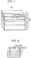
- Fig. 1 is a perspective view, partially in section, of a light emitting portion of one embodiment of a semiconductor laser constructed in accordance with the present invention.
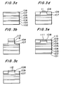
- Fig. 2 is an enlarged cross-sectional view of the active MQW layer in the semiconductor laser shown in Fig. 1.
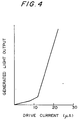
- Fig. 3 is a cross-sectional view illustrating the process of making the semiconductor laser shown in Fig. 1.
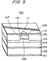
- Fig. 4 is a graph illustrating the relationship between the drive current and the generated light output in the semiconductor laser shown in Fig. 1.
- Fig. 5 is a perspective view, partially in section, of a light emitting portion of another embodiment of a semiconductor laser constructed in accordance with the present invention.
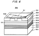
- Fig. 6 is a schematic cross-section of a light emitting portion of a surface emission type semiconductor laser constructed in accordance with the present invention, the semiconductor laser adapted to generate laser beams synchronized in phase.
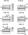
- Fig. 7 is a cross-sectional view of the semiconductor laser shown in Fig. 6, illustrating the process of making it.
- Fig. 8 illustrates differences in shape and near field pattern between the surface emission type semiconductor laser constructed according to the prior art and the semiconductor laser of Fig. 6:
- Fig. 8(a) shows the shape of the surface emission type semiconductor laser of the prior art on the exit side thereof;
- Fig. 8(b) shows an intensity profile in the near field pattern of the semiconductor laser shown in Fig. 8(a);
- Fig. 8(c) shows the shape of the semiconductor laser of the present embodiment at the exit side;
- Fig. 8(d) shows an intensity profile of the near field pattern of the semiconductor laser shown in Fig. 8(c).
- Figs. 9 (a) to (m) schematically illustrate various shapes of surface emission type semiconductor lasers constructed according to further embodiments of the present invention at the exit sides thereof.
- Figs. 10(a) to (d) schematically illustrate various shapes of surface emission type semiconductor lasers constructed according to still further embodiments of the present invention at the exit sides thereof.
- Figs. 11(a) to (c) schematically illustrate various shapes of surface emission type semiconductor lasers constructed according to other embodiments of the present invention at the exit sides thereof.
- Fig. 12 is a perspective view of a surface emission type semiconductor laser constructed according to the prior art, illustrating the light emitting portion thereof.
- FIGs. 1 and 2 there is shown a semiconductor laser 100 constructed in accordance with one embodiment of the present invention.
- the semiconductor laser 100 comprises a substrate of n-type GaAs 102 over which a buffer layer of n-type GaAs 103 is formed. Over the buffer layer 103, there are formed 30 pairs of distribution reflection type multi-layer film mirror 104 which include an n-type Al 0.7 Ga 0.3 As layer and an n-type Al 0.1 Ga 0.9 As layer and have a reflectivity equal to or higher than 98% against light rays having their wavelength substantially equal to 870 nm. On the multi-layer film mirror 104, there are sequentially formed a cladding layer of n-type Al 0.4 Ga 0.6 As 105, an active layer of multi-quantum well structure 106.
- the active MQW layer 106 comprises three well layers 106a, as shown in Fig. 2. Each of the well layers 106a is sandwiched between a pair of upper and lower barrier layers 106b. Each of the well layers 106a may be formed as of an i-type GaAs film having a thickness equal to 120 Angstroms while each of the barrier layers 106b may be formed as of an i-type Ga 0.65 Al 0.35 As film having a thickness equal to 150 Angstroms.
- the MOCVD process was carried out under such a condition that the temperature on growth is 700 ° C and the pressure on growth is 150 Torr. and used organic metals such as TMGa (trimethyl gallium) and TMA1(trimethyl aluminum) as III- group materials, AsH3 as V-group material, H2 Se as n-type dopant and DEZn (diethyl zinc) as p-type dopant.
- organic metals such as TMGa (trimethyl gallium) and TMA1(trimethyl aluminum) as III- group materials, AsH3 as V-group material, H2 Se as n-type dopant and DEZn (diethyl zinc) as p-type dopant.
- an SiO2 layer 112 is formed on the top of the multi-layered structure by the thermal CVD process.
- the multi-layered structure is etched up to the middle of the cladding layer of p-type Al 0.4 Ga 0.6 As 107, leaving a column-like light emitting portion covered with a hard baked resist layer 113 (Fig. 3(b)).
- the etching gas is a mixture of chlorine with argon under a pressure of 1 ⁇ 10 ⁇ 3 Torr..
- the leading voltage used therein is equal to 400 V.
- the purpose of the etching of the cladding layer 107 up to the middle thereof is to provide a rib waveguide type refraction waveguide structure which can confine injected carriers and light rays in the active layer.
- a layer of ZnS 0.06 Se 0.94 109 which is in lattice alignment with GaAs is then formed by causing this layer to grow around the column-like portion using the MBE or MOCVD process (Fig. 3(c)).
- a p-type ohmic electrode 110 is deposited on all the top face except the multi-layered dielectric film mirror 111.
- An n-type ohmic electrode 101 is further deposited over the bottom face of the semiconductor substrate 102.
- the entire structure is alloyed at 420 ° C to provide a surface emission type semiconductor laser (Fig. 3(e)).
- the surface emission type semiconductor laser thus formed provides a very effective current restriction since the buried layer 109 of ZnS 0.06 Se 0.94 has a resistance equal to or higher than one G ⁇ and there is no injection current into the buried layer.
- the active MQW layer 106 contributes to the reduction of generating threshold current. Since it is not required that the buried layer is any multi-layered structure, it can be more easily grown with an increased reproductiveness from one batch to another.
- the utilization of the rib waveguide structure using the ZnS 0.06 Se 0.94 layer having its refractive index sufficiently smaller than that of GaAs can realize a more effective light confinement.
- Fig. 4 shows the relationship between the drive current and the generated light output in the surface emission type semiconductor laser according to this embodiment.
- the continuous generation of laser beam can be accomplished in room temperature with a threshold level as very low as 10 ⁇ A by using the buried layer of II-VI group compound semiconductor 109 and the active MQW layer 106. If any active MQW layer is not used, the continuous generation of laser beam can be attained, but the threshold current will be as large as one mA.
- the active MQW layer serves to provide a light output at least five times higher than a case where no active layer of MQW structure is taken, for example, 25 mW or higher. Furthermore, the external differential quantum efficiency is increased and the characteristics of the laser is improved by restricting the reactive current.
- the cross-sectional shape of the column-like portion in the surface emission type semiconductor laser according to this embodiment of the present invention is of a circle or regular polygon such as square or regular octagon, a finely circular spot of beam can be provided.
- this cross-sectional shape is of any configuration other than the above ones, such as rectangle or trapezoid, the cross-section of the laser beam will be ellipse or multi-mode. This is not desirable in applying the semiconductor laser to the devices.
- Table 1 Diameter of Column Cross-Section Mode of Near Filed Pattern 2 ⁇ m Zero-Order Basic Mode 5 ⁇ m Zero-Order Basic Mode 10 ⁇ m Zero-Order Basic Mode 12 ⁇ m First-Order Mode 15 ⁇ m First-Order Mode
- Table 1 shows the relationship of near field pattern relative to the diameter of the cross-section of the column-like portion in the surface emission type semiconductor laser according to this embodiment of the present invention. It will be apparent therefrom that if the diameter is equal to or less than 10 ⁇ m, the generation is carried out in the basic mode.
- the contact layer 108 in the surface emission type semiconductor laser according to this embodiment of the present invention is of a thickness equal to or less than 3.0 ⁇ m. This is because of reduction of the light absorption in the contact layer. Such a thickness is more preferably less than 0.3 ⁇ m because the element resistance is reduced and the external differential quantum efficiency is increased.
- the present invention can be applied to a buried type refractive index waveguide structure as shown in Fig. 5, rather than the aforementioned rib waveguide type refractive index waveguide structure.
- the column-like semiconductor layers are formed to extend to the underlying cladding layer 105.
- the active MQW layer 106 will also be formed into a column-like configuration and enclosed by the buried layer 109.
- a phase-synchronization type semiconductor laser 300 constructed in accordance with the present invention, which can increase the dimension of the emission spot.
- the semiconductor laser 300 comprises a substrate of n-type GaAs 302 over which a buffer layer of n-type GaAs 303 is formed. Over the buffer layer 303, there are formed 25 pairs of distribution reflection type multi-layer film mirror 304 which includes an n-type Al 0.9 Ga 0.1 As layer and an n-type Al 0.2 Ga 0.8 As layer and have a reflectivity equal to or higher than 98% against light rays having their wavelength substantially equal to 780 ⁇ 30 nm.
- the multi-layer film mirror 304 there are sequentially formed a cladding layer of n-type Al 0.5 Ga 0.5 As 305, a waveguide layer 315, an active layer of multi-quantum well structure 306, another cladding layer of p-type Al 0.5 Ga 0.5 As 307 and a contact layer of p-type Al 0.15 Ga 0.85 As 308, utilizing the epitaxial growth in the MOCVD process (see Fig. 7(a)).
- the active MQW layer 306 comprises three well layers 306a, each of which is sandwiched between a pair of upper and lower barrier layers 306b, as shown in Fig. 2.
- Each of the well layers 306a may be formed of an i-type Ga 0.65 Al 0.35 As film having a thickness equal to 80 Angstroms while each of the barrier layers 306b is made of an i-type Ga 0.95 Al 0.05 As film having a thickness equal to 60 Angstroms.
- the waveguide layer 315 has a composition of Al ranged between those of the well and barrier layers 306a, 306b and may be formed of an n-type epitaxial layer of Ga 0.75 Al 0.25 As.
- Such a waveguide layer has a refractive index lower than the equivalent refractive index of the active MQW layer 306 but higher than the refractive index of the underlying cladding layer 305.
- the MOCVD process may be carried out as under such a condition that the temperature on growth is 720 ° C and the pressure on growth is 150 Torr. and used organic metals such as TMGa (trimethyl gallium) and TMAl(trimethyl aluminum) as III- group materials, AsH 3 as V-group material, H 2 Se as n-type dopant and DEZn (diethyl zinc) as p-type dopant.
- organic metals such as TMGa (trimethyl gallium) and TMAl(trimethyl aluminum) as III- group materials, AsH 3 as V-group material, H 2 Se as n-type dopant and DEZn (diethyl zinc) as p-type dopant.
- a SiO2 layer is formed on the top of the multi-layered structure in the atmospheric pressure by the thermal CVD process.
- a photoresist is then applied over the SiO2 layer and baked at a raised temperature to form a hard baked resist.
- a further SiO2 layer is formed over the hard baked resist by the EB deposition.
- the respective layers formed on the substrate are then etched by the use of reactive ion etching process (RIE process).
- RIE process reactive ion etching process
- the SiO2 layer formed on the hard baked resist 313 is first subjected to the conventional photolithograph to form a necessary resist pattern.
- This resist pattern is then used as a mask to perform the RIE process against the SiO2 layer.
- the RIE process may be carried out by using CF4 gas under a pressure of 4.5 Pa and an input RF power of 150 W and by controlling the sample holder at 20° C.
- This SiO2 layer is then utilized as a mask to etch the hard baked resist 313 by the RIE process which uses, for example, O2 gas under a pressure of 4.5 Pa and an input power of 150 W and controls the sample holder at 20° C.
- the resist pattern initially formed on the SiO2 layer is also etched.
- the etching is again performed by the use of CF4 gas.
- the thin SiO2 layer as a mask and performing the RIE process which is one of the dry etching processes against the hard baked resist 313, the latter may include side walls perpendicular to the substrate while maintaining the necessary pattern (Fig. 7(b)).
- the hard baked resist 313 having such vertical side walls is used as a mask in the reactive ion beam etching (RIBE) process so that the cladding layer of p-type Al 0.5 Ga 0.5 As 307 is etched up to its middle, leaving a plurality of column-like light emitting portions (Fig. 7(c)).
- the etching gas used herein is a mixture of chlorine with argon under a pressure equal to 5 ⁇ 10 ⁇ 4 Torr. and a plasma generating voltage equal to 400 V.
- the RIBE process is carried out at the current density of ion equal to 400 ⁇ A/cm on the etching sample while maintaining the sample holder at 20° C.
- etching the cladding layer 307 up to its middle is to provide a refraction waveguide type rib waveguide structure for confining the horizontal injection carriers and light rays in the active MQW layer 306 such that a part of the light rays can be transmitted in the horizontal direction within the active layer. Also in this embodiment, the propagation of light in the horizontal direction may be assured by the waveguide layer 315.
- the light emitting portions 320 arranged closed to each other can be separated from each other by a separation groove 314 and at the same time it is possible to produce a vertical light resonator which is required to improve the characteristics of the surface emission type semiconductor laser.
- the MBE or MOCVD process is used to grow a layer of ZnS 0.06 Se 0.94 309 around the light emitting portions, such a buried layer serving as a II-VI group compound epitaxial layer which is in lattice alignment with Al 0.5 Ga 0.5 As (Fig. 7(d)).
- This buried layer 309 is transparent for the generation wavelength of the surface emission type semiconductor laser 300.
- the SiO2 layer and polycrystalline ZnSSe produced thereon are removed.
- four pairs of multi-layered dielectric film mirror 311 made of SiO2 / ⁇ -Si are formed on the top of the multi-layered structure by means of electron beam deposition. Dry etching is then used to remove a part of the mirror 311 (Fig. 7(e)).
- the reflectivity of the multi-layered dielectric film mirror at wavelength of 780 nm is 95% or more. Since the multi-layered dielectric film mirror 311 is also formed over the separation groove 314 buried with ZnSSe, a vertical resonator structure also is formed at the region between the adjacent light emitting portions. As a result, light rays leaked into the separation groove 314 effectively contributes to the laser generation. Since the leaked light rays are utilized, the emitted light can be synchronized with the phase at the light emitting portions 320.
- a p-type ohmic electrode 310 is deposited on the top face except the multi-layered dielectric film mirror 311.
- An n-type ohmic electrode 301 is deposited on the bottom face of the substrate.
- the structure thus formed is alloyed at 420 ° C in the atmosphere of N2 to complete the surface emission type semiconductor laser 300 (Fig. 7(f)).
- the n-type ohmic electrode 310 on the exit side is formed to connect with the contact layer 308 in each of the light emitting portion.
- the surface emission type semiconductor laser produced according to this embodiment utilizes the epitaxial ZnSSe layer 309 as a buried layer, it can have a resistance equal to or higher than one G ⁇ , which is higher than that of the prior art blocking structure using a counter bias at the p-n junction in the AlGaAs layer. This provides an optimum current blocking structure. As a result, the generating threshold current can be reduced.
- the active MQW layer 306 also serves to reduce the generating threshold current, for example, to a level of about ten ⁇ A.
- the light emitting portions 320 separated from each other by the separation groove 314 can be influenced by each other through the active and waveguide layers 306 and 315.
- light rays from the respective light emitting portions 320 can be synchronized with each other in phase, resulting in generation of a laser beam having an increased diameter and an emphasized intensity. Moreover, the light leaked from the light emitting portion 320 can be effectively utilized since the buried layer is made of a transparent material having less absorption for the generation wavelength of 780 nm.
- Fig. 8 shows the arrangements of the surface emission type semiconductor lasers constructed respectively in accordance with the prior art and the present invention at the exit sides thereof and intensity profiles of NFP when the laser beam is generated.
- Fig. 8(a) shows that the resonators 620 of the prior art surface emission type semiconductor laser 600 shown in Fig. 12 are arranged close to one another up to a distance by which the resonators can be fully covered by the epitaxial layers of GaAlAs 607 and 608 connected with each other at the n-p junction, that is, a distance equal to about 5 ⁇ m.
- the exit face of the laser actually includes the multi-layered dielectric film mirror and the p-type ohmic electrode formed thereon, they are omitted in Fig. 8 for clear illustration.
- Fig. 8(b) shows an intensity profile of NFP between points a and b in Fig. 8(a).
- the prior art surface emission type semiconductor laser only provides a plurality of adjacent light spots even if a plurality of light emitting portions 620 are arranged closed to each other.
- Fig. 8(c) shows the arrangement of the exit end of the surface emission type semiconductor laser constructed according to this embodiment wherein the separation groove is buried with a ZnS 0.06 Se 0.94 layer 309 which formed by the vapor-phase epitaxy method.
- the minimum width of the separation groove can be equal to one ⁇ m.
- Fig. 8(d) shows NFP between points c and d in Fig. 8(c). It will be apparent from this NFP that the light emission spot is enlarged since light rays exit also from above the separation groove 314. Since the adjacent laser beams are synchronized with each other in phase, the light output can be increased with an angle of radiation being equal to or less than one degree.
- Table 2 shows the relationship between the width of the separation groove of the surface emission type semiconductor laser 300 and the order of transverse generation mode measured from NFP.
- Table 2 Width of Separation Groove Mode of Near Filed Pattern 0.5 ⁇ m Zero-Order Basic Mode 1.0 ⁇ m Zero-Order Basic Mode 5.0 ⁇ m Zero-Order Basic Mode 10 ⁇ m First-Order Mode 20 ⁇ m Higher-Order Mode
- the width of the separation groove is less than 10 ⁇ m.
- the transverse generation mode of the laser synchronized in phase is in the basic mode. If the width is equal to or more than 10 ⁇ m. the laser will be generated in an order equal to or higher than one. In this case, the laser beam will be of an elliptic configuration with its increased angle of radiation. This is undesirable in all the applications. If the separation groove has a width less than 0.5 ⁇ m, the laser beam will not be circular.
- each of the optical resonators has a p-type ohmic electrode at its exit side, a laser beam from each optical resonator may be independently controlled with respect to ON, OFF and modulation.
- Figs. 9 to 11 show the other embodiments of the present invention in which various configurations and arrangements of optical resonators and associated separation grooves in a plane parallel to the substrate as viewed from the exit side are schematically illustrated.
- Figs. 9(a) - (j) and (m) represent line symmetry arrangements in which a plurality of column-like semiconductor layers each having a circular or regularly polygonal cross-section parallel to the substrate are formed.
- the light emitting spot formed by any one of such arrangements can have a dimension larger than that of a light emitting spot formed by a single light emitting portion.
- the cross-section of each of the light emitting portions may be any configuration other than circle or regular polygon.
- the essential requirement in the concept of the present invention is that a non-circular or non-polygonal line joining the outer edges of the light emitting portions arranged in line symmetry approximate to a circular or regularly polygonal configuration. So the configurations shown in Figs. (k) and (l) are suitable for generating the laser beam having larger diamiter.
- Figs. (k) and (l) are suitable for generating the laser beam having larger diamiter.
- a line beam may be provided by disposing a plurality of light emitting portions in row and/or column on a two-dimensional plane parallel to the substrate.
- a semiconductor laser which comprises a plurality of spaced p-type ohmic electrodes 310 equal in number to the light omitting portions 320, these electrodes 310 being connected with the contact layer 308.
- each of the light emitting portions will be generate a beam having a circular cross-section which can be independently controlled in ON, OFF and modulation, these beams being synchronized with one another in phase.
- the surface emission type semiconductor laser of the present invention may be equivalently applied to any desirable light source in various devices such as printer, copying machine, facsimile, display and so on.
Landscapes
- Physics & Mathematics (AREA)
- Condensed Matter Physics & Semiconductors (AREA)
- General Physics & Mathematics (AREA)
- Electromagnetism (AREA)
- Optics & Photonics (AREA)
- Semiconductor Lasers (AREA)
Claims (18)
- Oberflächenemittierender Halbleiterlaser zur Emission eines Laserstrahls in einer Richtung senkrecht zu einem Halbleitersubstrat (102), umfassend:eine optische Resonatoranordnung, die ein Paar reflektierender Spiegel (104, 111) mit unterschiedlichem Reflexionsvermögen enthält,eine Vielzahl von III-V-Halbleiterschichten (105, 106, 107) zwischen den reflektierenden Spiegeln, wobei die Halbleiterschichten wenigstens eine Mantelschicht (107) enthalten, die zu wenigstens einem säulenartigen Abschnitt geformt ist, undeine vergrabene Schicht (109) zur Stromeingrenzung, die um den säulenartigen Abschnitt ausgebildet ist,dadurch gekennzeichnet, daß die vergrabene Schicht eine aus der Dampfphase gewachsene Epitaxialschicht eines II-VI-Verbindungshalbleiters aus drei oder vier Elementen, ausgewählt aus den Elementen Zn, Cd und Hg der II. Gruppe und den Elementen O, S, Se und Te der VI. Gruppe, ist, undeine aktive Schicht (106) eines Multi-Quantum-Well-Aufbaus am unteren Schichtabschnitt der Mantelschicht (107) mit dem säulenartigen Aufbau ausgebildet ist, wobei die aktive Schicht eine Vielzahl von Well-Schichten (106a) enthält, von denen jede zwischen Sperrschichten (106b) eingeschlossen ist.
- Halbleiterlaser nach Anspruch 1, bei dem der Querschnitt des säulenartigen Abschnitts parallel zu dem Halbleitersubstrat (102) eine kreisförmige oder regelmäßig polygonale Gestalt aufweist.
- Halbleiterlaser nach Anspruch 2, bei dem der säulenartige Abschnitt entweder einen Durchmesser oder Diagonallinien gleich oder weniger als 10 µm in Ebenen parallel zu dem Halbleitersubstrat (102) aufweist.
- Halbleiterlaser nach einem der Ansprüche 1 bis 3, bei dem eine Halbleiterkontaktschicht (108) der optischen Resonatoranordnung an deren Austrittsseite eine Dicke gleich oder geringer als 3,0 µm aufweist.
- Halbleiterlaser nach einem der Ansprüche 1 bis 4, bei dem die optische Resonatoranordnung einen säulenartigen Abschnitt enthält, und bei dem einer der reflektierenden Spiegel (111) an der Austrittsseite gegenüber der Stirnfläche des säulenartigen Abschnitts innerhalb des Bereichs der Stirnfläche ausgebildet ist.
- Halbleiterlaser nach Anspruch 5, bei dem die optische Resonatoranordnung eine Brechungsindex-Wellenleiterstruktur des Rippen-Wellenleitertyps aufweist, wobei der Rippen-Wellenleiter von der aktiven Schicht (106) des Multi-Quantum-Well-Aufbaus gebildet ist.
- Halbleiterlaser nach Anspruch 5, bei dem der säulenartige Abschnitt die aktive Schicht (106) des Multi-Quantum-Well-Aufbaus zur Bildung einer Brechungsindex-Wellenleiterstruktur des vergrabenen Typs enthält.
- Halbleiterlaser nach einem der Ansprüche 1 bis 4, bei dem die optische Resonatoranordnung eine Trennutanordnung (314) zum Trennen einer Mehrzahl der säulenartigen Abschnitte voneinander enthält, die II-VI-Verbindungshalbleiter-Epitaxialschicht (309) in der Trennutanordnung zur Bildung eines Lichtemissionsabschnitts auf jedem der säulenartigen Abschnitte vergraben ist, und die aktive Schicht (306) als gemeinsame Schicht für alle lichtemittierenden Abschnitte ausgebildet ist, wodurch Lichtstrahlen von den lichtemittierenden Abschnitten miteinander phasensynchronisiert werden können.
- Halbleiterlaser nach Anspruch 8, bei dem die Trennutanordnung (314) Seitenwände aufweist, die sich senkrecht zu dem Halbleitersubstrat erstrecken.
- Halbleiterlaser nach Anspruch 8 oder 9, bei dem die Trennutanordnung (314) mit der II-VI-Verbindungshalbleiter-Epitaxialschicht (309), die für die Wellenlänge des emittierten Laserstrahls transparent ist, vergraben ist, und bei dem der reflektierende Spiegel (311) an der Austrittsseite über einem Bereich gegenüber den Stirnflächen der säulenartigen Abschnitte und der in der Trennutanordnung vergrabenen II-VI-Verbindungshalbleiter-Epitaxialschicht ausgebildet ist.
- Halbleiterlaser nach Anspruch 10, bei dem die II-VI-Verbindungshalbleiter-Epitaxialschicht aus irgendeinem aus der Gruppe bestehend aus ZnSSe, ZnCdS und CdSSe gebildet ist.
- Halbleiterlaser nach Anspruch 10 oder 11, bei dem die Breite der Trennutanordnung (314) in einer Richtung parallel zu dem Halbleitersubstrat gleich oder größer ist als 0,5 µm und kleiner ist als 10 µm.
- Halbleiterlaser nach einem der Ansprüche 10 bis 12, bei dem jeder der säulenartigen Abschnitte einen kreisförmigen oder regelmäßig polygonalen Querschnitt in einer zweidimensionalen Ebene parallel zu dem Halbleitersubstrat aufweist, und bei dem eine Mehrzahl der säulenartigen Abschnitte in Liniensymmetrie in der zweidimensionalen Ebene zur Emission eines Laserstrahls mit einem kreisförmigen Querschnitt angeordnet sind.
- Halbleiterlaser nach einem der Ansprüche 10 bis 12, bei dem jeder der säulenartigen Abschnitte einen nicht-kreisförmigen oder nicht-polygonalen Querschnitt in einer zweidimensionalen Ebene parallel zu dem Halbleitersubstrat aufweist, und bei dem die äußeren Kanten der säulenartigen Abschnitte zur Bildung im wesentlichen eines kreisförmigen oder regelmäßig polygonalen Profils angeordnet sind, wodurch ein Laserstrahl mit einem kreisförmigen Querschnitt von dem Halbleiterlaser emittiert werden kann.
- Halbleiterlaser nach einem der Ansprüche 10 bis 12, bei dem eine Mehrzahl der optischen Resonatoranordnungen, jeweils von einer Mehrzahl der säulenartigen Abschnitte definiert, auf dem Halbleitersubstrat ausgebildet ist, um eine unabhängige Elektrode in jeder der optischen Resonatoranordnungen auf der Austrittsseite zu schaffen, wodurch ein von der optischen Resonatoranordnung emittierter und einen kreisförmigen Querschnitt aufweisender Laserstrahl, der in der Lage ist, einen vergrößerten Lichtemissionsfleck zu bilden, unabhängig in EIN, AUS und Modulation gesteuert werden kann.
- Halbleiterlaser nach einem der Ansprüche 10 bis 12, bei dem eine Mehrzahl der säulenartigen Abschnitte mit gleichem Abstand in einer Reihe und/oder Spalte angeordnet sind, um einen von ihnen in Form eines Linienstrahls emittierten Laserstrahl zu schaffen.
- Halbleiterlaser nach einem der Ansprüche 1 bis 16, ferner umfassend eine Wellenleiterschicht (315), die an dem unteren Schichtabschnitt der aktiven Schicht (306) des Multi-Quantum-Well-Aufbaus ausgebildet ist, wobei die Wellenleiterschicht so beschaffen ist, daß sie Lichtstrahlen in einer Richtung parallel zur aktiven Schicht ausbreitet.
- Halbleiterlaser nach Anspruch 17, bei dem der Brechungsindex der Wellenleiterschicht (315) niedriger ist als der äquivalente Brechungsindex der aktiven Schicht (306), aber höher ist als der Brechungsindex der Mantelschicht unterhalb der Wellenleiterschicht.
Applications Claiming Priority (2)
| Application Number | Priority Date | Filing Date | Title |
|---|---|---|---|
| JP24200090 | 1990-09-12 | ||
| JP242000/90 | 1990-09-12 |
Publications (3)
| Publication Number | Publication Date |
|---|---|
| EP0475372A2 EP0475372A2 (de) | 1992-03-18 |
| EP0475372A3 EP0475372A3 (en) | 1992-08-05 |
| EP0475372B1 true EP0475372B1 (de) | 1996-01-03 |
Family
ID=17082765
Family Applications (3)
| Application Number | Title | Priority Date | Filing Date |
|---|---|---|---|
| EP91115316A Expired - Lifetime EP0475371B1 (de) | 1990-09-12 | 1991-09-10 | Oberflächenemittierender Halbleiterlaser und Verfahren zu seiner Herstellung |
| EP91115318A Expired - Lifetime EP0475373B1 (de) | 1990-09-12 | 1991-09-10 | Oberflächenemittierender Halbleiterlaser |
| EP91115317A Expired - Lifetime EP0475372B1 (de) | 1990-09-12 | 1991-09-10 | Oberflächenemittierender Halbleiterlaser |
Family Applications Before (2)
| Application Number | Title | Priority Date | Filing Date |
|---|---|---|---|
| EP91115316A Expired - Lifetime EP0475371B1 (de) | 1990-09-12 | 1991-09-10 | Oberflächenemittierender Halbleiterlaser und Verfahren zu seiner Herstellung |
| EP91115318A Expired - Lifetime EP0475373B1 (de) | 1990-09-12 | 1991-09-10 | Oberflächenemittierender Halbleiterlaser |
Country Status (5)
| Country | Link |
|---|---|
| US (3) | US5182757A (de) |
| EP (3) | EP0475371B1 (de) |
| KR (3) | KR100210290B1 (de) |
| DE (3) | DE69118066T2 (de) |
| TW (1) | TW229338B (de) |
Families Citing this family (45)
| Publication number | Priority date | Publication date | Assignee | Title |
|---|---|---|---|---|
| US5404369A (en) * | 1990-09-12 | 1995-04-04 | Seiko Epson Corporation | Surface emission type semiconductor laser |
| US5295148A (en) * | 1990-09-12 | 1994-03-15 | Seiko Epson Corporation | Surface emission type semiconductor laser |
| US5317584A (en) * | 1990-09-12 | 1994-05-31 | Seiko Epson Corporation | Surface emission type semiconductor laser |
| US5356832A (en) * | 1990-09-12 | 1994-10-18 | Seiko Epson Corporation | Method of making surface emission type semiconductor laser |
| US5537666A (en) * | 1990-09-12 | 1996-07-16 | Seiko Epson Coropration | Surface emission type semiconductor laser |
| US5436922A (en) * | 1990-09-12 | 1995-07-25 | Seiko Epson Corporation | Surface emission type semiconductor laser |
| DE69207521T2 (de) * | 1991-03-28 | 1996-09-05 | Seiko Epson Corp | Senkrecht zur Oberfläche emittierender Halbleiterlaser und Verfahren zu seiner Herstellung |
| DE69232124T2 (de) * | 1991-05-14 | 2002-03-14 | Seiko Epson Corp., Tokio/Tokyo | Bilderzeugungsgerät |
| KR950007490B1 (ko) * | 1991-12-28 | 1995-07-11 | 엘지전자주식회사 | 반도체 레이저 |
| US5341001A (en) * | 1992-02-13 | 1994-08-23 | Matsushita Electric Industrial Co., Ltd. | Sulfide-selenide manganese-zinc mixed crystal photo semiconductor and laser diode |
| US5245622A (en) * | 1992-05-07 | 1993-09-14 | Bandgap Technology Corporation | Vertical-cavity surface-emitting lasers with intra-cavity structures |
| US5351255A (en) * | 1992-05-12 | 1994-09-27 | North Carolina State University Of Raleigh | Inverted integrated heterostructure of group II-VI semiconductor materials including epitaxial ohmic contact and method of fabricating same |
| JPH065975A (ja) * | 1992-06-22 | 1994-01-14 | Matsushita Electric Ind Co Ltd | 半導体レーザ |
| JP3095545B2 (ja) * | 1992-09-29 | 2000-10-03 | 株式会社東芝 | 面発光型半導体発光装置およびその製造方法 |
| JPH0722646A (ja) * | 1993-06-30 | 1995-01-24 | Mitsubishi Chem Corp | 電流ブロック層を有するled |
| SE501722C2 (sv) * | 1993-09-10 | 1995-05-02 | Ellemtel Utvecklings Ab | Ytemitterande laseranordning med vertikal kavitet |
| SE501721C2 (sv) * | 1993-09-10 | 1995-05-02 | Ellemtel Utvecklings Ab | Laseranordning med i en optisk kavitet seriekopplade laserstrukturer |
| WO1995020254A1 (en) * | 1994-01-20 | 1995-07-27 | Seiko Epson Corporation | Surface emission type semiconductor laser, method and apparatus for producing the same |
| JP3452982B2 (ja) * | 1994-08-24 | 2003-10-06 | ローム株式会社 | Ledプリントヘッド、およびledアレイチップ、ならびにそのledアレイチップの製造方法 |
| US5778018A (en) * | 1994-10-13 | 1998-07-07 | Nec Corporation | VCSELs (vertical-cavity surface emitting lasers) and VCSEL-based devices |
| US5838705A (en) * | 1996-11-04 | 1998-11-17 | Motorola, Inc. | Light emitting device having a defect inhibition layer |
| KR100322061B1 (ko) * | 1998-07-01 | 2002-03-08 | 김순택 | Crt용반도체레이저스크린 |
| KR100322060B1 (ko) * | 1998-07-01 | 2002-03-08 | 김순택 | Crt용반도체레이저스크린및그제조방법 |
| US6291839B1 (en) | 1998-09-11 | 2001-09-18 | Lulileds Lighting, U.S. Llc | Light emitting device having a finely-patterned reflective contact |
| DE19911433B4 (de) | 1999-03-04 | 2006-06-08 | Infineon Technologies Ag | Optische Sendeanordnung |
| US6879427B2 (en) | 2000-04-10 | 2005-04-12 | Lenslet Ltd. | Shear inducing beamsplitter for interferometric image processing |
| US7170919B2 (en) * | 2003-06-23 | 2007-01-30 | Northrop Grumman Corporation | Diode-pumped solid-state laser gain module |
| KR100714639B1 (ko) * | 2003-10-21 | 2007-05-07 | 삼성전기주식회사 | 발광 소자 |
| JP2006128475A (ja) * | 2004-10-29 | 2006-05-18 | Mitsubishi Electric Corp | 半導体レーザ |
| KR100638732B1 (ko) * | 2005-04-15 | 2006-10-30 | 삼성전기주식회사 | 수직구조 질화물 반도체 발광소자의 제조방법 |
| US8373153B2 (en) | 2009-05-26 | 2013-02-12 | University Of Seoul Industry Cooperation Foundation | Photodetectors |
| US8367925B2 (en) * | 2009-06-29 | 2013-02-05 | University Of Seoul Industry Cooperation Foundation | Light-electricity conversion device |
| US8395141B2 (en) * | 2009-07-06 | 2013-03-12 | University Of Seoul Industry Cooperation Foundation | Compound semiconductors |
| US8748862B2 (en) * | 2009-07-06 | 2014-06-10 | University Of Seoul Industry Cooperation Foundation | Compound semiconductors |
| US8809834B2 (en) | 2009-07-06 | 2014-08-19 | University Of Seoul Industry Cooperation Foundation | Photodetector capable of detecting long wavelength radiation |
| US8227793B2 (en) | 2009-07-06 | 2012-07-24 | University Of Seoul Industry Cooperation Foundation | Photodetector capable of detecting the visible light spectrum |
| US8368990B2 (en) | 2009-08-21 | 2013-02-05 | University Of Seoul Industry Cooperation Foundation | Polariton mode optical switch with composite structure |
| US8368047B2 (en) * | 2009-10-27 | 2013-02-05 | University Of Seoul Industry Cooperation Foundation | Semiconductor device |
| US8058641B2 (en) | 2009-11-18 | 2011-11-15 | University of Seoul Industry Corporation Foundation | Copper blend I-VII compound semiconductor light-emitting devices |
| US10186676B2 (en) * | 2017-03-13 | 2019-01-22 | Intel Corporation | Emissive devices for displays |
| US10651527B2 (en) | 2017-08-22 | 2020-05-12 | Qorvo Us, Inc. | Spatial power-combining devices with segmented waveguides and antennas |
| WO2020026573A1 (ja) * | 2018-07-31 | 2020-02-06 | ソニー株式会社 | 面発光半導体レーザ |
| KR102515120B1 (ko) * | 2019-01-21 | 2023-03-29 | 한온시스템 주식회사 | 스크롤 압축기 |
| CN114946093A (zh) * | 2020-01-08 | 2022-08-26 | 索尼集团公司 | 发光元件及其制造方法和发光元件阵列 |
| CN113675726A (zh) * | 2021-10-21 | 2021-11-19 | 福建慧芯激光科技有限公司 | 一种高速垂直腔面发射激光器的外延结构 |
Family Cites Families (10)
| Publication number | Priority date | Publication date | Assignee | Title |
|---|---|---|---|---|
| JPS6179280A (ja) * | 1984-09-27 | 1986-04-22 | Agency Of Ind Science & Technol | 面発光型半導体レ−ザ装置及びその製造方法 |
| FR2606223B1 (fr) * | 1986-10-29 | 1996-03-01 | Seiko Epson Corp | Laser a semiconducteur et son procede de fabrication |
| JPH01125990A (ja) * | 1987-11-11 | 1989-05-18 | Mitsubishi Electric Corp | 半導体発光装置 |
| JPH01264285A (ja) * | 1988-04-15 | 1989-10-20 | Omron Tateisi Electron Co | 面発光型半導体レーザ |
| JPH01266779A (ja) * | 1988-04-19 | 1989-10-24 | Canon Inc | 面発光レーザ |
| US5031187A (en) * | 1990-02-14 | 1991-07-09 | Bell Communications Research, Inc. | Planar array of vertical-cavity, surface-emitting lasers |
| US5045897A (en) * | 1990-03-14 | 1991-09-03 | Santa Barbara Research Center | Quaternary II-VI materials for photonics |
| US5052016A (en) * | 1990-05-18 | 1991-09-24 | University Of New Mexico | Resonant-periodic-gain distributed-feedback surface-emitting semiconductor laser |
| US5068868A (en) * | 1990-05-21 | 1991-11-26 | At&T Bell Laboratories | Vertical cavity surface emitting lasers with electrically conducting mirrors |
| US5086430A (en) * | 1990-12-14 | 1992-02-04 | Bell Communications Research, Inc. | Phase-locked array of reflectivity-modulated surface-emitting lasers |
-
1991
- 1991-09-09 US US07/756,981 patent/US5182757A/en not_active Expired - Lifetime
- 1991-09-09 US US07/756,979 patent/US5181219A/en not_active Expired - Lifetime
- 1991-09-09 US US07/756,980 patent/US5181221A/en not_active Expired - Lifetime
- 1991-09-10 EP EP91115316A patent/EP0475371B1/de not_active Expired - Lifetime
- 1991-09-10 EP EP91115318A patent/EP0475373B1/de not_active Expired - Lifetime
- 1991-09-10 EP EP91115317A patent/EP0475372B1/de not_active Expired - Lifetime
- 1991-09-10 DE DE69118066T patent/DE69118066T2/de not_active Expired - Lifetime
- 1991-09-10 DE DE69118065T patent/DE69118065T2/de not_active Expired - Lifetime
- 1991-09-10 DE DE69116038T patent/DE69116038T2/de not_active Expired - Lifetime
- 1991-09-12 KR KR1019910016033A patent/KR100210290B1/ko not_active Expired - Lifetime
- 1991-09-12 KR KR1019910016034A patent/KR100210289B1/ko not_active Expired - Lifetime
- 1991-09-12 KR KR1019910016035A patent/KR100210288B1/ko not_active Expired - Lifetime
- 1991-09-14 TW TW080107294A patent/TW229338B/zh not_active IP Right Cessation
Non-Patent Citations (2)
| Title |
|---|
| CONFERENCE DIGEST OF THE 11TH IEEE INTERNATIONAL SEMICONDUCTOR LASER CONFERENCE August 1988, Boston, Massachusetts, US, pages 164 - 165; A. IBARAKI et al.: 'GaAs/GaA1As DBR surface emitting laser with GaA1As/A1As and SiO2/TiO2 reflectors' * |
| LECTURES OF THE 50TH MEETING OF APPLIED PHYSICS IN JAPAN (1989), vol. 3, page 909 (29-ZG-7) * |
Also Published As
| Publication number | Publication date |
|---|---|
| KR100210288B1 (ko) | 1999-07-15 |
| DE69118066D1 (de) | 1996-04-25 |
| KR100210290B1 (ko) | 1999-07-15 |
| DE69118065T2 (de) | 1996-09-19 |
| TW229338B (de) | 1994-09-01 |
| DE69116038D1 (de) | 1996-02-15 |
| EP0475371A2 (de) | 1992-03-18 |
| EP0475372A2 (de) | 1992-03-18 |
| KR920007282A (ko) | 1992-04-28 |
| US5181219A (en) | 1993-01-19 |
| DE69116038T2 (de) | 1996-06-20 |
| DE69118065D1 (de) | 1996-04-25 |
| EP0475373A3 (en) | 1992-08-12 |
| EP0475373A2 (de) | 1992-03-18 |
| KR100210289B1 (ko) | 1999-07-15 |
| US5182757A (en) | 1993-01-26 |
| DE69118066T2 (de) | 1996-09-19 |
| EP0475373B1 (de) | 1996-03-20 |
| KR920007281A (ko) | 1992-04-28 |
| EP0475371B1 (de) | 1996-03-20 |
| KR920007283A (ko) | 1992-04-28 |
| EP0475372A3 (en) | 1992-08-05 |
| US5181221A (en) | 1993-01-19 |
| EP0475371A3 (en) | 1992-08-05 |
Similar Documents
| Publication | Publication Date | Title |
|---|---|---|
| EP0475372B1 (de) | Oberflächenemittierender Halbleiterlaser | |
| US5062115A (en) | High density, independently addressable, surface emitting semiconductor laser/light emitting diode arrays | |
| EP0709939B1 (de) | Licht-emittierende Vorrichtung und Verfahren zu ihrer Herstellung | |
| US7787511B2 (en) | Array of surface-emitting laser diodes having reduced device resistance and capable of performing high output operation and method of fabricating the surface-emitting laser diode | |
| US5557627A (en) | Visible-wavelength semiconductor lasers and arrays | |
| EP0858137B1 (de) | Oberflächenemittierende Laservorrichtung und ihr Herstellungsverfahren | |
| US5348912A (en) | Semiconductor surface emitting laser having enhanced optical confinement | |
| US5699375A (en) | Multiple wavelength, surface emitting laser with broad bandwidth distributed Bragg reflectors | |
| EP1233493B1 (de) | Oberflächenemittierender Laser mit vertikalem Resonator und mit einer Abstandsschicht zur effizienten Diffusion von Löchern zwischen der p-Elektrode und der aktiven Schicht und dessen Herstellungsverfahren | |
| US5963576A (en) | Annular waveguide vertical cavity surface emitting laser and method of fabrication | |
| US5295148A (en) | Surface emission type semiconductor laser | |
| US5587335A (en) | Method of making surface emission type semiconductor laser | |
| JPH06224518A (ja) | サーフェススキミングレーザを作るためのモノリシック半導体デバイス | |
| US5317584A (en) | Surface emission type semiconductor laser | |
| JP2628801B2 (ja) | 半導体レーザ構造体 | |
| JP2857256B2 (ja) | 垂直型半導体レーザ | |
| JP3395194B2 (ja) | 面発光型半導体レーザ | |
| JP3206097B2 (ja) | 面発光型半導体レーザ | |
| US5404369A (en) | Surface emission type semiconductor laser | |
| US5625637A (en) | Surface emitting semiconductor laser and its manufacturing process | |
| JP3206080B2 (ja) | 半導体レーザ | |
| US5436922A (en) | Surface emission type semiconductor laser | |
| US5356832A (en) | Method of making surface emission type semiconductor laser | |
| US4447905A (en) | Current confinement in semiconductor light emitting devices | |
| JP3240636B2 (ja) | 面発光型半導体レーザ |
Legal Events
| Date | Code | Title | Description |
|---|---|---|---|
| PUAI | Public reference made under article 153(3) epc to a published international application that has entered the european phase |
Free format text: ORIGINAL CODE: 0009012 |
|
| AK | Designated contracting states |
Kind code of ref document: A2 Designated state(s): DE FR GB NL |
|
| PUAL | Search report despatched |
Free format text: ORIGINAL CODE: 0009013 |
|
| AK | Designated contracting states |
Kind code of ref document: A3 Designated state(s): DE FR GB NL |
|
| 17P | Request for examination filed |
Effective date: 19921013 |
|
| RIN1 | Information on inventor provided before grant (corrected) |
Inventor name: ASAKA, TATSUYA Inventor name: IWANO, HIDEAKI Inventor name: MORI, KATSUMI |
|
| 17Q | First examination report despatched |
Effective date: 19930621 |
|
| GRAA | (expected) grant |
Free format text: ORIGINAL CODE: 0009210 |
|
| AK | Designated contracting states |
Kind code of ref document: B1 Designated state(s): DE FR GB NL |
|
| REF | Corresponds to: |
Ref document number: 69116038 Country of ref document: DE Date of ref document: 19960215 |
|
| ET | Fr: translation filed | ||
| PLBE | No opposition filed within time limit |
Free format text: ORIGINAL CODE: 0009261 |
|
| STAA | Information on the status of an ep patent application or granted ep patent |
Free format text: STATUS: NO OPPOSITION FILED WITHIN TIME LIMIT |
|
| 26N | No opposition filed | ||
| REG | Reference to a national code |
Ref country code: GB Ref legal event code: IF02 |
|
| PGFP | Annual fee paid to national office [announced via postgrant information from national office to epo] |
Ref country code: FR Payment date: 20100921 Year of fee payment: 20 |
|
| PGFP | Annual fee paid to national office [announced via postgrant information from national office to epo] |
Ref country code: GB Payment date: 20100908 Year of fee payment: 20 |
|
| PGFP | Annual fee paid to national office [announced via postgrant information from national office to epo] |
Ref country code: NL Payment date: 20100916 Year of fee payment: 20 |
|
| PGFP | Annual fee paid to national office [announced via postgrant information from national office to epo] |
Ref country code: DE Payment date: 20100908 Year of fee payment: 20 |
|
| REG | Reference to a national code |
Ref country code: DE Ref legal event code: R071 Ref document number: 69116038 Country of ref document: DE |
|
| REG | Reference to a national code |
Ref country code: DE Ref legal event code: R071 Ref document number: 69116038 Country of ref document: DE |
|
| REG | Reference to a national code |
Ref country code: NL Ref legal event code: V4 Effective date: 20110910 |
|
| REG | Reference to a national code |
Ref country code: GB Ref legal event code: PE20 Expiry date: 20110909 |
|
| PG25 | Lapsed in a contracting state [announced via postgrant information from national office to epo] |
Ref country code: GB Free format text: LAPSE BECAUSE OF EXPIRATION OF PROTECTION Effective date: 20110909 |
|
| PG25 | Lapsed in a contracting state [announced via postgrant information from national office to epo] |
Ref country code: NL Free format text: LAPSE BECAUSE OF EXPIRATION OF PROTECTION Effective date: 20110910 |
|
| PG25 | Lapsed in a contracting state [announced via postgrant information from national office to epo] |
Ref country code: DE Free format text: LAPSE BECAUSE OF EXPIRATION OF PROTECTION Effective date: 20110911 |