EP0709939B1 - Licht-emittierende Vorrichtung und Verfahren zu ihrer Herstellung - Google Patents
Licht-emittierende Vorrichtung und Verfahren zu ihrer Herstellung Download PDFInfo
- Publication number
- EP0709939B1 EP0709939B1 EP95116057A EP95116057A EP0709939B1 EP 0709939 B1 EP0709939 B1 EP 0709939B1 EP 95116057 A EP95116057 A EP 95116057A EP 95116057 A EP95116057 A EP 95116057A EP 0709939 B1 EP0709939 B1 EP 0709939B1
- Authority
- EP
- European Patent Office
- Prior art keywords
- region
- substrate
- mirror
- buffer
- type
- Prior art date
- Legal status (The legal status is an assumption and is not a legal conclusion. Google has not performed a legal analysis and makes no representation as to the accuracy of the status listed.)
- Expired - Lifetime
Links
- 238000000034 method Methods 0.000 title claims description 13
- 238000004519 manufacturing process Methods 0.000 title description 4
- 239000000758 substrate Substances 0.000 claims description 61
- 239000002019 doping agent Substances 0.000 claims description 27
- 229910001218 Gallium arsenide Inorganic materials 0.000 description 13
- 125000004429 atom Chemical group 0.000 description 13
- 230000015572 biosynthetic process Effects 0.000 description 8
- XUIMIQQOPSSXEZ-UHFFFAOYSA-N Silicon Chemical compound [Si] XUIMIQQOPSSXEZ-UHFFFAOYSA-N 0.000 description 6
- 239000004065 semiconductor Substances 0.000 description 6
- 229910052710 silicon Inorganic materials 0.000 description 6
- 239000010703 silicon Substances 0.000 description 6
- 238000005253 cladding Methods 0.000 description 5
- 238000001451 molecular beam epitaxy Methods 0.000 description 5
- 229910000980 Aluminium gallium arsenide Inorganic materials 0.000 description 4
- 229910000530 Gallium indium arsenide Inorganic materials 0.000 description 4
- HCHKCACWOHOZIP-UHFFFAOYSA-N Zinc Chemical group [Zn] HCHKCACWOHOZIP-UHFFFAOYSA-N 0.000 description 4
- 238000003491 array Methods 0.000 description 4
- 239000000463 material Substances 0.000 description 4
- 229910052725 zinc Inorganic materials 0.000 description 4
- 239000011701 zinc Substances 0.000 description 4
- OKTJSMMVPCPJKN-UHFFFAOYSA-N Carbon Chemical compound [C] OKTJSMMVPCPJKN-UHFFFAOYSA-N 0.000 description 2
- 229910052799 carbon Inorganic materials 0.000 description 2
- 230000004888 barrier function Effects 0.000 description 1
- 238000004140 cleaning Methods 0.000 description 1
- 238000004891 communication Methods 0.000 description 1
- 238000011109 contamination Methods 0.000 description 1
- 230000008878 coupling Effects 0.000 description 1
- 238000010168 coupling process Methods 0.000 description 1
- 238000005859 coupling reaction Methods 0.000 description 1
- 230000007547 defect Effects 0.000 description 1
- 238000000151 deposition Methods 0.000 description 1
- 238000005516 engineering process Methods 0.000 description 1
- 238000005530 etching Methods 0.000 description 1
- 125000004435 hydrogen atom Chemical group [H]* 0.000 description 1
- 239000007943 implant Substances 0.000 description 1
- 239000002184 metal Substances 0.000 description 1
- 229910052751 metal Inorganic materials 0.000 description 1
- 230000003287 optical effect Effects 0.000 description 1
- 230000006798 recombination Effects 0.000 description 1
- 238000005215 recombination Methods 0.000 description 1
- 230000002269 spontaneous effect Effects 0.000 description 1
Images




Classifications
-
- H—ELECTRICITY
- H10—SEMICONDUCTOR DEVICES; ELECTRIC SOLID-STATE DEVICES NOT OTHERWISE PROVIDED FOR
- H10H—INORGANIC LIGHT-EMITTING SEMICONDUCTOR DEVICES HAVING POTENTIAL BARRIERS
- H10H20/00—Individual inorganic light-emitting semiconductor devices having potential barriers, e.g. light-emitting diodes [LED]
- H10H20/80—Constructional details
- H10H20/81—Bodies
- H10H20/822—Materials of the light-emitting regions
- H10H20/824—Materials of the light-emitting regions comprising only Group III-V materials, e.g. GaP
-
- H—ELECTRICITY
- H01—ELECTRIC ELEMENTS
- H01S—DEVICES USING THE PROCESS OF LIGHT AMPLIFICATION BY STIMULATED EMISSION OF RADIATION [LASER] TO AMPLIFY OR GENERATE LIGHT; DEVICES USING STIMULATED EMISSION OF ELECTROMAGNETIC RADIATION IN WAVE RANGES OTHER THAN OPTICAL
- H01S5/00—Semiconductor lasers
- H01S5/10—Construction or shape of the optical resonator, e.g. extended or external cavity, coupled cavities, bent-guide, varying width, thickness or composition of the active region
- H01S5/18—Surface-emitting [SE] lasers, e.g. having both horizontal and vertical cavities
- H01S5/183—Surface-emitting [SE] lasers, e.g. having both horizontal and vertical cavities having only vertical cavities, e.g. vertical cavity surface-emitting lasers [VCSEL]
- H01S5/18308—Surface-emitting [SE] lasers, e.g. having both horizontal and vertical cavities having only vertical cavities, e.g. vertical cavity surface-emitting lasers [VCSEL] having a special structure for lateral current or light confinement
-
- H—ELECTRICITY
- H10—SEMICONDUCTOR DEVICES; ELECTRIC SOLID-STATE DEVICES NOT OTHERWISE PROVIDED FOR
- H10H—INORGANIC LIGHT-EMITTING SEMICONDUCTOR DEVICES HAVING POTENTIAL BARRIERS
- H10H20/00—Individual inorganic light-emitting semiconductor devices having potential barriers, e.g. light-emitting diodes [LED]
- H10H20/01—Manufacture or treatment
- H10H20/011—Manufacture or treatment of bodies, e.g. forming semiconductor layers
- H10H20/013—Manufacture or treatment of bodies, e.g. forming semiconductor layers having light-emitting regions comprising only Group III-V materials
-
- H—ELECTRICITY
- H10—SEMICONDUCTOR DEVICES; ELECTRIC SOLID-STATE DEVICES NOT OTHERWISE PROVIDED FOR
- H10H—INORGANIC LIGHT-EMITTING SEMICONDUCTOR DEVICES HAVING POTENTIAL BARRIERS
- H10H20/00—Individual inorganic light-emitting semiconductor devices having potential barriers, e.g. light-emitting diodes [LED]
- H10H20/80—Constructional details
- H10H20/81—Bodies
- H10H20/813—Bodies having a plurality of light-emitting regions, e.g. multi-junction LEDs or light-emitting devices having photoluminescent regions within the bodies
-
- H—ELECTRICITY
- H01—ELECTRIC ELEMENTS
- H01S—DEVICES USING THE PROCESS OF LIGHT AMPLIFICATION BY STIMULATED EMISSION OF RADIATION [LASER] TO AMPLIFY OR GENERATE LIGHT; DEVICES USING STIMULATED EMISSION OF ELECTROMAGNETIC RADIATION IN WAVE RANGES OTHER THAN OPTICAL
- H01S5/00—Semiconductor lasers
- H01S5/02—Structural details or components not essential to laser action
- H01S5/0206—Substrates, e.g. growth, shape, material, removal or bonding
- H01S5/0207—Substrates having a special shape
-
- H—ELECTRICITY
- H01—ELECTRIC ELEMENTS
- H01S—DEVICES USING THE PROCESS OF LIGHT AMPLIFICATION BY STIMULATED EMISSION OF RADIATION [LASER] TO AMPLIFY OR GENERATE LIGHT; DEVICES USING STIMULATED EMISSION OF ELECTROMAGNETIC RADIATION IN WAVE RANGES OTHER THAN OPTICAL
- H01S5/00—Semiconductor lasers
- H01S5/04—Processes or apparatus for excitation, e.g. pumping, e.g. by electron beams
- H01S5/042—Electrical excitation ; Circuits therefor
- H01S5/0421—Electrical excitation ; Circuits therefor characterised by the semiconducting contacting layers
-
- H—ELECTRICITY
- H01—ELECTRIC ELEMENTS
- H01S—DEVICES USING THE PROCESS OF LIGHT AMPLIFICATION BY STIMULATED EMISSION OF RADIATION [LASER] TO AMPLIFY OR GENERATE LIGHT; DEVICES USING STIMULATED EMISSION OF ELECTROMAGNETIC RADIATION IN WAVE RANGES OTHER THAN OPTICAL
- H01S5/00—Semiconductor lasers
- H01S5/10—Construction or shape of the optical resonator, e.g. extended or external cavity, coupled cavities, bent-guide, varying width, thickness or composition of the active region
- H01S5/18—Surface-emitting [SE] lasers, e.g. having both horizontal and vertical cavities
- H01S5/183—Surface-emitting [SE] lasers, e.g. having both horizontal and vertical cavities having only vertical cavities, e.g. vertical cavity surface-emitting lasers [VCSEL]
- H01S5/18305—Surface-emitting [SE] lasers, e.g. having both horizontal and vertical cavities having only vertical cavities, e.g. vertical cavity surface-emitting lasers [VCSEL] with emission through the substrate, i.e. bottom emission
-
- H—ELECTRICITY
- H01—ELECTRIC ELEMENTS
- H01S—DEVICES USING THE PROCESS OF LIGHT AMPLIFICATION BY STIMULATED EMISSION OF RADIATION [LASER] TO AMPLIFY OR GENERATE LIGHT; DEVICES USING STIMULATED EMISSION OF ELECTROMAGNETIC RADIATION IN WAVE RANGES OTHER THAN OPTICAL
- H01S5/00—Semiconductor lasers
- H01S5/20—Structure or shape of the semiconductor body to guide the optical wave ; Confining structures perpendicular to the optical axis, e.g. index or gain guiding, stripe geometry, broad area lasers, gain tailoring, transverse or lateral reflectors, special cladding structures, MQW barrier reflection layers
- H01S5/2054—Methods of obtaining the confinement
- H01S5/2059—Methods of obtaining the confinement by means of particular conductivity zones, e.g. obtained by particle bombardment or diffusion
- H01S5/2063—Methods of obtaining the confinement by means of particular conductivity zones, e.g. obtained by particle bombardment or diffusion obtained by particle bombardment
-
- H—ELECTRICITY
- H01—ELECTRIC ELEMENTS
- H01S—DEVICES USING THE PROCESS OF LIGHT AMPLIFICATION BY STIMULATED EMISSION OF RADIATION [LASER] TO AMPLIFY OR GENERATE LIGHT; DEVICES USING STIMULATED EMISSION OF ELECTROMAGNETIC RADIATION IN WAVE RANGES OTHER THAN OPTICAL
- H01S5/00—Semiconductor lasers
- H01S5/30—Structure or shape of the active region; Materials used for the active region
- H01S5/305—Structure or shape of the active region; Materials used for the active region characterised by the doping materials used in the laser structure
- H01S5/3054—Structure or shape of the active region; Materials used for the active region characterised by the doping materials used in the laser structure p-doping
-
- H—ELECTRICITY
- H01—ELECTRIC ELEMENTS
- H01S—DEVICES USING THE PROCESS OF LIGHT AMPLIFICATION BY STIMULATED EMISSION OF RADIATION [LASER] TO AMPLIFY OR GENERATE LIGHT; DEVICES USING STIMULATED EMISSION OF ELECTROMAGNETIC RADIATION IN WAVE RANGES OTHER THAN OPTICAL
- H01S5/00—Semiconductor lasers
- H01S5/30—Structure or shape of the active region; Materials used for the active region
- H01S5/305—Structure or shape of the active region; Materials used for the active region characterised by the doping materials used in the laser structure
- H01S5/3095—Tunnel junction
-
- H—ELECTRICITY
- H01—ELECTRIC ELEMENTS
- H01S—DEVICES USING THE PROCESS OF LIGHT AMPLIFICATION BY STIMULATED EMISSION OF RADIATION [LASER] TO AMPLIFY OR GENERATE LIGHT; DEVICES USING STIMULATED EMISSION OF ELECTROMAGNETIC RADIATION IN WAVE RANGES OTHER THAN OPTICAL
- H01S5/00—Semiconductor lasers
- H01S5/40—Arrangement of two or more semiconductor lasers, not provided for in groups H01S5/02 - H01S5/30
- H01S5/42—Arrays of surface emitting lasers
- H01S5/423—Arrays of surface emitting lasers having a vertical cavity
Definitions
- the present invention relates generally to light emitting devices, in particular to surface emitting lasers and more specifically to formation of an n-drive p-common laser fabricated on an n-type substrate.
- a second class of laser diodes is fabricated such that the laser structure is perpendicular to the surface of the semiconductor wafer so that the emitted light is perpendicular to the surface.
- These laser diodes are commonly known as surface emitting lasers (SELs).
- Both classes of lasers are formed on a starting substrate which may be either semi-insulating, p-type or n-type.
- a starting substrate which may be either semi-insulating, p-type or n-type.
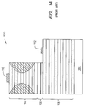
- FIG 1A shows a cross-sectional view of a conventional n-drive SEL 100 formed on a semi-insulating substrate 102.
- the surface emitting laser 100 may be viewed as a n-i-p diode comprised of an n-type mirror region 104, an active region 106, and a p-type mirror region 108. Electrical connection is made via electrode 110 formed on the top surface of the n-type mirror region 104 and electrode 112 formed on the p-type mirror region 108.
- an etch is made through both the n-type mirror region 104 and the active region 106 to the p-type region 108. This is problematic since the p-type contact etch exposes epitaxial layers 104, 106, 108 which have a tendency to oxidize. Further, the p-type contact etch creates a non-planar structure creating device reliability problems and increasing manufacturing complexity. Further, defects added to semi-insulating substrates to make the substrate isolating reduce the reliability of the semiconductor laser device.
- FIG. 1B shows a cross-sectional view of a conventional n-drive surface emitting laser 120 formed on a p-type substrate 122.
- the SEL is comprised of a n-type mirror region 124, an active region 126, and a p-type mirror region 128. Electrical interconnections are made via electrode 130 formed on the surface of the n-type mirror region 124 and electrode 132 formed on the surface of the p-type substrate 122.
- the preferred method of formation for the n, i, and p-type regions is by molecular beam epitaxy.
- the only commonly available p-type substrate is zinc doped.
- Figure 1C shows a cross-sectional view of a surface emitting laser 140 formed on an n-type substrate 142.
- the SEL is comprised of a n-type mirror region 144, an active region 146, and a p-type mirror region 148.
- the SEL 140 shown in Figure 1C is a p-drive SEL.
- the p-drive SEL is typically voltage driven.
- current drivers for p-drive SELs exist, they are problematic.
- the available silicon pnp drivers typically have insufficient speed for current data rates of optical communication systems and GaAs pnp drivers are expensive.
- Voltage driven p-drive SELs in SEL arrays require precise control so that the V f of each individual laser in the array is uniform. Nonuniformities in V f require individually pre-biasing each individual laser in the laser array; thereby increasing the cost of the laser drivers.
- n-drive SELs may be created from the structure shown in Figure 1C by sawing between individual lasers and flipping the p-drive SELs. However, this eliminates the possibility of SEL arrays.
- a method of forming an array of n-drive semiconductor laser on a n-type substrate is needed.
- the IEEE Lasers and Electrooptics Society 1993, Annual Meeting, Conference proceedings, 15 November 1993, pages 564 and 565 discloses vertical-cavity laser diodes comprising an active region including three active quantum wells for generating light, the active region having a first and a second surface, an n-top reflector for reflecting light towards the active quantum wells, the first n-top reflector being located on the first surface of the active region, a second p-bottom reflector having a second conductivity type and a first and second opposite surface, the second reflector reflecting lights towards the quantum wells.
- the first and the second surface of the second reflector being located on the second surface of the active quantum wells.
- the laser diode comprises a substrate having a first and second surface. The first surface of the substrate is located on the second surface of the second reflector.
- the invention is based on the object of providing a light emitting device which does not suffer from the above-explained reliability problems and of providing a process for forming such a light-emitting device.
- Figure 1A shows a cross-sectional view of a conventional n-drive surface emitting laser formed on a semi-insulating substrate.
- Figure 1B shows a cross-sectional view of a conventional n-drive surface emitting laser formed on a p-type substrate
- Figure 1C shows a cross-sectional view of a p-drive surface emitting laser formed on a n-type substrate.
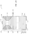
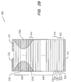
- Figures 2A and 2B show a cross-sectional view of the n-drive SEL fabricated on a n-type substrate according to the preferred embodiment of the present invention.
- Figures 3A and 3B show a cross-sectional view of the n-drive SEL fabricated on a n-type substrate according to an alternative embodiment of the present invention.
- FIG. 2 shows a cross-sectional view of the n-drive SEL 200 fabricated on a n-type substrate 202 according to the preferred embodiment of the present invention.
- Figure 2A shows a bottom emitting n-drive SEL.
- Figure 2B shows a top emitting n-drive SEL.
- the n-drive SEL 200 shown is comprised of an active region 204, first and second mirror regions 206, 208 located on opposite sides of the active region, a buffer region 210, and a substrate 202.
- the SEL 200 may be viewed as a n-i-p diode having an n-type mirror region 206, an active region 204, and a p-type mirror region 208.
- the substrate 202 and the first mirror region 206 have a first conductivity type.
- the second mirror region 208 and the buffer region 210 are of a second opposite conductivity type.
- the first conductivity type is n-type.
- the preferred embodiment provides a method of forming an n-drive semiconductor laser on an n-type substrate.
- the first and second mirrors 206, 208 both have a first and second side.
- the active region 204 is located between the first and second mirrors 206, 208 such that the first side of the first mirror region is adjacent to the first side of the active region and the first side of the second mirror is adjacent to the second opposite side of the active region.
- the buffer region 210 is located between the substrate region and the second mirror region such that the first side of the buffer region is adjacent to the the second side of the second mirror region and the second side of the buffer region is adjacent to the first side of the substrate region.
- the first and second mirror regions 206, 208 are constructed from alternating layers having different indices of refraction using techniques well known in the art.
- the thickness of each layer is chosen to be 1/4 of the wavelength of light to be emitted.
- the alternating layers form Bragg mirrors.
- the alternating layers are typically constructed of AlAs and GaAs or AlGaAs.
- the light generation region 209 of the active region 204 generates light due to spontaneous and stimulated emission via the recombination of electrons and holes generated by forward biasing the n-i-p diode.
- the light generation region 209 of the light emitting device 200 shown in Figure 2 is typically constructed of one or more quantum wells of InGaAs, GaAs, AlGaAs, or InAlGaAs which are separated from the first and second mirror regions 206, 208 by cladding regions 211a, 211b.
- the choice and thickness of the material depends on the desired wavelength of the light emitted by the SEL 200.
- the junction 216 formed between the buffer region 210 and the substrate 202 forms a tunnel contact.
- the buffer region 210 is typically comprised of a first layer 220 having a first dopant concentration and a second degeneratively doped layer 218 having a second dopant concentration.
- the tunnel diode is reversed biased so that application of a voltage to electrode contacts 212, 214 injects current through the degeneratively doped p-n junction 216.
- the tunnel diode is reverse biased by applying a negative voltage to contact 212 and coupling contact 214 to ground.
- the SEL shown in Figures 2 and 3 are not to scale.
- the mirror regions 206, 208 and the active region 204 have been expanded to provide clarity in the drawings.
- the thickness of the substrate region 202 is approximately 150 ⁇ m as compared to about a 10 ⁇ m combined thickness of the mirror regions 206, 208, the active regions 204, and the buffer region 210.
- Electrodes 212, 214 are approximately 10 ⁇ m in diameter, while electrode 214 has an opening of approximately 20 - 150 ⁇ m.
- An array of SELs can be constructed by depositing a plurality of layers on the substrate 202.
- the layers are deposited by molecular beam epitaxy.
- the substrate region 202 is comprised of three layers.
- the first layer 221, is the GaAs substrate.
- the GaAs is doped with an n-type dopant, preferably silicon, and has a silicon dopant concentration typically in the range of 5 x 10 17 to 5 x 10 19 atoms/cm 3 .
- the third layer 224 of the substrate region 202 is a degeneratively doped n-type layer typically having a thickness in the range of 100 to 1000 ⁇ and a dopant concentration in the range of approximately 5 x 10 17 to 1 x 10 19 atoms/cm 3 .
- the buffer region 210 is typically comprised of two layers 218, 220, grown by molecular beam epitaxy having different dopant concentrations.
- the first layer 218 is a p-type very degeneratively doped GaAs layer typically doped with carbon having a dopant concentration in the range of 1 x 10 19 to 1 x 10 21 atoms/cm 3 and a thickness in the range of 100 to 1000 ⁇ .
- the preferred dopant concentration is 1 x 10 20 atoms/cm 3 and the preferred thickness is 200 ⁇ .
- the second layer 220 of the buffer region 210 is a typically GaAs doped with carbon having a dopant concentration in the range of 5 x 10 17 to 1 x 10 20 atoms/cm 3 and a thickness in the range of 1000 to 5000 ⁇ .
- the preferred dopant concentration is 5 x 10 19 atoms/cm 3 and the preferred thickness is 3000 ⁇ .
- the dopant concentration of the first layer 218 of the buffer region is given as in the range of 1 x 10 19 to 1 x 10 21 atoms/cm 3 , the dopant concentration may be higher.
- the 1 x 10 21 atoms/cm 3 is more a function of what is reasonably attainable by current process technology than limitations required for formation of a tunnel contact.
- the material used in forming the substrate region 202 and the buffer region may also vary.
- some of the layers may be comprised of InGaAs or another bandgap material.
- the substrate region the third layer 224 of the substrate region and the first layer 218 of the buffer region may be degeneratively doped InGaAs. Using InGaAs at the tunnel junction 216 provides a lower tunnel voltage.
- the second mirror region 208 is comprised of alternating p-type layers having different indices of refraction.
- the thickness of each layer is chosen to be one quarter of the lasing wavelength. Assuming a lasing wavelength of 980 nm each of the alternating layers in the mirror region would have a thickness of 9800 ⁇ /n where n is the refractive index of the layer.
- the active region 204 is formed.
- the thickness of active region 204 should be the lasing wavelength or a multiple of the lasing wavelength.
- the active region 204 is comprised of an light generation region 209 positioned between first and second confinement or cladding regions 211a, 211b.
- the first cladding layer 211a is p-doped AlGaAs having a preferred dopant concentration of 5 x 10 17 atoms/cm 3 and a thickness of approximately 1000 ⁇ .
- the light generation region 209 is comprised of alternating GaAs barrier layers and In .2 Ga .8 As layers (not shown) forming quantum well structures.
- a second cladding region 211b is formed.
- the second cladding region is typically n-doped AlGaAs having a n-type dopant concentration of 5 x 10 17 atoms/cm 3 and a thickness of approximately 1000 ⁇ .
- the first mirror region 206 is formed.
- the first mirror region 206 is comprised of alternating n-type layers having different indices of refraction and a thickness equal to one quarter of the lasing wavelength. In the preferred embodiment, there are 15 pairs of alternating layers.
- the alternating layers are AlAs doped with silicon having a dopant concentration of 1 x 10 18 atoms/cm 3 and GaAs doped with silicon having a dopant concentration 1 x 10 18 atoms/cm 3 .
- Regions 230 of the first mirror region 206 may be converted to regions of high resistivity by an implant step. Typically, this is accomplished by implanting with hydrogen atoms.
- FIG. 2A shows a bottom emitting SEL including a tunnel junction 216 formed between the n-type substrate 202 and the p-type buffer region 210.
- n-contacts 214 are made to the bottom surface of the n+ substrate 202.
- N-contact 212 is made to the top surface of the n-type mirror region 206.
- Figure 2B shows a top emitting SEL.
- the top emitting SEL is similar to the bottom emitting laser shown in Figure 2A, however, the bottom emitting SEL typically includes a phase matching layer 236 not found in the top emitting SEL.
- Figure 3 shows a cross-sectional view of the n-drive SEL fabricated on a n-type substrate according to an alternative embodiment of the present invention.
- the alternative embodiment includes a light generation region 304, first and second mirror regions 306, 308 located on opposite sides of the light generation region 304 where the second mirror region 306 has a first side and a second side, a buffer region 310 being located on the second side of the second mirror region 306, and a substrate 302.
- the embodiments shown in Figure 3 include a buffer region 310, in the alternative embodiment a tunnel junction is not formed between the buffer region 310 and the substrate 302.
- Figure 3A shows a bottom emitting SEL according to the alternative embodiment.
- Figure 3B shows a top emitting SEL according to an alternative embodiment of the present invention.
- p-contact is not made using a tunnel contact but instead is made using a via to the buffer region 310.
- P-contact 314 is made by etching through the n-type mirror region 306, the active region 304, and the p-type mirror region 304 to the surface of the p-type buffer region 310 and forming a metal contact 312.
- p-contact 314 can be made by performing a bottom etch through the n+ substrate layer 302 to the p-type buffer region 310.
- a junction 316 is formed between the substrate 302 and the buffer region 310.
- a tunnel contact is not formed.
- the dopant concentration differential at the junction 316 is not critical.
- the substrate region 302 is comprised solely of an n-type GaAs substrate and the buffer region and the buffer region is comprised of a single p-type doped GaAs layer.
Landscapes
- Physics & Mathematics (AREA)
- Condensed Matter Physics & Semiconductors (AREA)
- General Physics & Mathematics (AREA)
- Electromagnetism (AREA)
- Optics & Photonics (AREA)
- Semiconductor Lasers (AREA)
Claims (6)
- Ein lichtemittierendes Bauelement (200) mit folgenden Merkmalen:wobei die Pufferregion (210; 310) und die Substratregion (202; 302) einen Tunnelkontakt bilden, und wobei der Tunnelkontakt in Sperrichtung vorgespannt ist.einer aktiven Region (204; 304), die eine Lichterzeugungsregion (209) zum Erzeugen von Licht als Reaktion auf Licht, das dieselbe durchtritt, aufweist, wobei die aktive Region eine erste Oberfläche und eine zweite gegenüberliegende Oberfläche aufweist;einer ersten Spiegelregion (206; 306) mit einem ersten Leitfähigkeitstyp, wobei die erste Spiegelregion (206; 306) zum Reflektieren von Licht zu der Lichterzeugungsregion (209) dient, wobei die erste Spiegelregion (206; 306) auf der ersten Oberfläche der aktiven Region positioniert ist;einer zweiten Spiegelregion (208; 308) mit einem zweiten Leitfähigkeitstyp und mit einer ersten und einer zweiten gegenüberliegenden Oberfläche, wobei die zweite Spiegelregion (208; 308) zum Reflektieren von Licht zu der Lichterzeugungsregion (209) hin dient, wobei die erste Oberfläche der zweiten Spiegelregion auf einer zweiten Oberfläche der aktiven Region positioniert ist;einer Pufferregion (210; 310) mit einer ersten Oberfläche und einer zweiten gegenüberliegenden Oberfläche, wobei die erste Oberfläche der Pufferregion auf der zweiten Oberfläche der zweiten Spiegelregion positioniert ist, wobei die Pufferregionschicht einen zweiten Leitfähigkeitstyp aufweist; undeiner Substratregion (202; 302) mit einer ersten und einer zweiten Oberfläche, wobei die erste Oberfläche der Substratregion auf der zweiten Oberfläche der Pufferregion positioniert ist, wobei die Substratregion einen ersten Leitfähigkeitstyp aufweist,
- Das Bauelement gemäß Anspruch 1, bei dem die Dotierstoffkonzentration des Abschnitts der Pufferregion (210; 310), der die Substratregion (202; 302) kontaktiert, degenerativ dotiert ist, und bei dem der Abschnitt der Substratregion, der die Pufferregion kontaktiert, degenerativ dotiert ist.
- Das Bauelement gemäß Anspruch 2, bei dem die Dotierstoffkonzentration der Pufferregion, die die Substratregion kontaktiert, in dem Bereich von 1 x 10¹⁹ bis 1 x 10²¹ Atome/cm3 liegt, und die Dotierstoffkonzentration des Abschnitts der Substratregion, der die Pufferregion kontaktiert, in dem Bereich von 5 x 10¹⁷ bis 5 x 10¹⁹ Atome/cm3 liegt.
- Ein Verfahren zum Herstellen eines lichtemittierenden Bauelements (200) mit folgenden Schritten:Bilden einer n-i-p-Diode, die Strom in einer Flußrichtung leitet, wobei die n-i-p-Diode durch folgende Schritte hergestellt wird:Bilden einer aktiven Region (204; 304), die eine Lichterzeugungsregion (209) zum Erzeugen von Licht als Reaktion auf Licht, das dieselbe durchtritt, aufweist, wobei die aktive Region eine erste Oberfläche und eine zweite Oberfläche aufweist, die der ersten Oberfläche gegenüberliegt,Bilden einer ersten Spiegelregion (206; 306) mit einem ersten Leitfähigkeitstyp, wobei die erste Spiegelregion zum Reflektieren von Licht zu der Lichterzeugungsregion (209) hin dient, wobei die erste Spiegelregion auf der ersten Oberfläche der aktiven Region positioniert ist, undBilden einer zweiten Spiegelregion (208; 308) mit einem zweiten Leitfähigkeitstyp, einer ersten Oberfläche und einer zweiten Oberfläche, die der ersten Oberfläche gegenüberliegt, wobei die zweite Spiegelregion zum Reflektieren von Licht zu der Lichterzeugungsregion (209) hin dient, wobei die erste Oberfläche der zweiten Spiegelregion auf der zweiten Oberfläche der aktiven Region positioniert ist;Bilden einer Pufferregion (210; 310) mit einer ersten Oberfläche und einer zweiten Oberfläche, die der ersten Oberfläche gegenüberliegt, wobei die erste Oberfläche der Pufferregion auf der zweiten Oberfläche der zweiten Spiegelregion positioniert ist, wobei die Pufferregionschicht einen zweiten Leitfähigkeitstyp aufweist, wobei der Schritt des Bildens der Pufferregion einen Schritt des degenerativen Dotierens eines Abschnitts (218) der Pufferregion benachbart zu der zweiten Oberfläche derselben aufweist; undBilden einer Substratregion (202; 302) mit einer ersten Oberfläche und einer zweiten Oberfläche, wobei die erste Oberfläche der Substratregion auf der zweiten Oberfläche der Pufferregion positioniert ist, wobei die Substratregion einen ersten Leitfähigkeitstyp aufweist, wobei der Schritt des Bildens der Substratregion einen Schritt des degenerativen Dotierens eines Abschnitts (224) der Substratregion benachbart zu der Pufferregion aufweist, wobei der Schritt des degenerativen Dotierens einen Tunnelkontakt (216) bildet, der durch den Strom in Sperrichtung vorgespannt ist, der durch die n-i-p-Diode in der Flußrichtung fließt.
- Das Verfahren gemäß Anspruch 4, bei dem der erste Leitfähigkeitstyp der n-Typ ist, während der zweite Leitfähigkeitstyp der p-Typ ist.
- Das Verfahren gemäß Anspruch 5, bei dem die Dotierstoffkonzentration der Pufferregion, die die Substratregion kontaktiert, in dem Bereich von 1 x 10¹⁹ bis 1 x 10²¹ Atome/cm3 liegt, und die Dotierstoffkonzentration des Abschnitts der Substratregion, die die Pufferregion kontaktiert, in dem Bereich von 5 x 10¹⁷ bis 5 x 10¹⁹ Atome/cm3 liegt.
Applications Claiming Priority (2)
| Application Number | Priority Date | Filing Date | Title |
|---|---|---|---|
| US330033 | 1994-10-27 | ||
| US08/330,033 US5892784A (en) | 1994-10-27 | 1994-10-27 | N-drive p-common surface emitting laser fabricated on n+ substrate |
Publications (2)
| Publication Number | Publication Date |
|---|---|
| EP0709939A1 EP0709939A1 (de) | 1996-05-01 |
| EP0709939B1 true EP0709939B1 (de) | 1998-08-26 |
Family
ID=23288021
Family Applications (1)
| Application Number | Title | Priority Date | Filing Date |
|---|---|---|---|
| EP95116057A Expired - Lifetime EP0709939B1 (de) | 1994-10-27 | 1995-10-11 | Licht-emittierende Vorrichtung und Verfahren zu ihrer Herstellung |
Country Status (4)
| Country | Link |
|---|---|
| US (1) | US5892784A (de) |
| EP (1) | EP0709939B1 (de) |
| JP (1) | JP3840276B2 (de) |
| DE (1) | DE69504276T2 (de) |
Families Citing this family (60)
| Publication number | Priority date | Publication date | Assignee | Title |
|---|---|---|---|---|
| US5892787A (en) * | 1994-10-27 | 1999-04-06 | Hewlett-Packard Company | N-drive, p-common light-emitting devices fabricated on an n-type substrate and method of making same |
| US5727014A (en) * | 1995-10-31 | 1998-03-10 | Hewlett-Packard Company | Vertical-cavity surface-emitting laser generating light with a defined direction of polarization |
| GB9524414D0 (en) * | 1995-11-29 | 1996-01-31 | Secr Defence | Low resistance contact semiconductor device |
| AU3600697A (en) * | 1996-08-09 | 1998-03-06 | W.L. Gore & Associates, Inc. | Vertical cavity surface emitting laser with tunnel junction |
| DE19703615A1 (de) * | 1997-01-31 | 1998-08-06 | Siemens Ag | Optoelektronisches Halbleiterbauelement |
| DE19703612A1 (de) | 1997-01-31 | 1998-08-06 | Siemens Ag | Halbleiterlaser-Bauelement |
| FR2761822B1 (fr) * | 1997-04-03 | 1999-05-07 | Alsthom Cge Alcatel | Laser semiconducteur a emission de surface |
| DE19723677A1 (de) | 1997-06-05 | 1998-12-10 | Siemens Ag | Optoelektronisches Halbleiterbauelement |
| US5936266A (en) * | 1997-07-22 | 1999-08-10 | The Board Of Trustees Of The University Of Illinois | Semiconductor devices and methods with tunnel contact hole sources |
| EP1014455B1 (de) | 1997-07-25 | 2006-07-12 | Nichia Corporation | Halbleitervorrichtung aus einer nitridverbindung |
| US6188711B1 (en) | 1997-12-18 | 2001-02-13 | Agilent Technologies, Inc. | Polarization-controlled VCSELs using externally applied uniaxial stress |
| DE19813727C2 (de) * | 1998-03-27 | 2000-04-13 | Siemens Ag | Vertikalresonator-Laserdiode und Verfahren zu deren Herstellung |
| DE19900816C2 (de) * | 1999-01-12 | 2001-04-26 | Siemens Ag | Vertikalresonator-Laserdiode mit optimierter aktiver Fläche, sowie Laserzeiger oder Laserpointer |
| JP3770014B2 (ja) | 1999-02-09 | 2006-04-26 | 日亜化学工業株式会社 | 窒化物半導体素子 |
| WO2000052796A1 (en) * | 1999-03-04 | 2000-09-08 | Nichia Corporation | Nitride semiconductor laser element |
| US6526082B1 (en) * | 2000-06-02 | 2003-02-25 | Lumileds Lighting U.S., Llc | P-contact for GaN-based semiconductors utilizing a reverse-biased tunnel junction |
| US6853663B2 (en) * | 2000-06-02 | 2005-02-08 | Agilent Technologies, Inc. | Efficiency GaN-based light emitting devices |
| US7065124B2 (en) * | 2000-11-28 | 2006-06-20 | Finlsar Corporation | Electron affinity engineered VCSELs |
| US6905900B1 (en) * | 2000-11-28 | 2005-06-14 | Finisar Corporation | Versatile method and system for single mode VCSELs |
| US6965626B2 (en) * | 2002-09-03 | 2005-11-15 | Finisar Corporation | Single mode VCSEL |
| US6813293B2 (en) * | 2002-11-21 | 2004-11-02 | Finisar Corporation | Long wavelength VCSEL with tunnel junction, and implant |
| JP2004288674A (ja) * | 2003-03-19 | 2004-10-14 | Fuji Xerox Co Ltd | 面発光型半導体レーザおよびそれを用いた光通信システム |
| US20040222363A1 (en) * | 2003-05-07 | 2004-11-11 | Honeywell International Inc. | Connectorized optical component misalignment detection system |
| JP3838218B2 (ja) | 2003-05-19 | 2006-10-25 | ソニー株式会社 | 面発光型半導体レーザ素子及びその製造方法 |
| US20040247250A1 (en) * | 2003-06-03 | 2004-12-09 | Honeywell International Inc. | Integrated sleeve pluggable package |
| US7298942B2 (en) | 2003-06-06 | 2007-11-20 | Finisar Corporation | Pluggable optical optic system having a lens fiber stop |
| US7433381B2 (en) | 2003-06-25 | 2008-10-07 | Finisar Corporation | InP based long wavelength VCSEL |
| US7277461B2 (en) * | 2003-06-27 | 2007-10-02 | Finisar Corporation | Dielectric VCSEL gain guide |
| US7075962B2 (en) * | 2003-06-27 | 2006-07-11 | Finisar Corporation | VCSEL having thermal management |
| US7054345B2 (en) | 2003-06-27 | 2006-05-30 | Finisar Corporation | Enhanced lateral oxidation |
| US7149383B2 (en) * | 2003-06-30 | 2006-12-12 | Finisar Corporation | Optical system with reduced back reflection |
| US6961489B2 (en) | 2003-06-30 | 2005-11-01 | Finisar Corporation | High speed optical system |
| US20060056762A1 (en) * | 2003-07-02 | 2006-03-16 | Honeywell International Inc. | Lens optical coupler |
| US20050013542A1 (en) * | 2003-07-16 | 2005-01-20 | Honeywell International Inc. | Coupler having reduction of reflections to light source |
| US7210857B2 (en) * | 2003-07-16 | 2007-05-01 | Finisar Corporation | Optical coupling system |
| US20050013539A1 (en) * | 2003-07-17 | 2005-01-20 | Honeywell International Inc. | Optical coupling system |
| US6887801B2 (en) * | 2003-07-18 | 2005-05-03 | Finisar Corporation | Edge bead control method and apparatus |
| US7031363B2 (en) * | 2003-10-29 | 2006-04-18 | Finisar Corporation | Long wavelength VCSEL device processing |
| US7372886B2 (en) * | 2004-06-07 | 2008-05-13 | Avago Technologies Fiber Ip Pte Ltd | High thermal conductivity vertical cavity surface emitting laser (VCSEL) |
| US7548675B2 (en) * | 2004-09-29 | 2009-06-16 | Finisar Corporation | Optical cables for consumer electronics |
| US7706692B2 (en) * | 2004-09-29 | 2010-04-27 | Finisar Corporation | Consumer electronics with optical communication interface |
| US7729618B2 (en) * | 2005-08-30 | 2010-06-01 | Finisar Corporation | Optical networks for consumer electronics |
| US7860398B2 (en) * | 2005-09-15 | 2010-12-28 | Finisar Corporation | Laser drivers for closed path optical cables |
| DE102006015788A1 (de) | 2006-01-27 | 2007-09-13 | Osram Opto Semiconductors Gmbh | Optoelektronischer Halbleiterchip |
| US7535034B2 (en) | 2006-02-27 | 2009-05-19 | The Board Of Trustees Of The University Of Illinois | PNP light emitting transistor and method |
| US7876989B2 (en) * | 2006-04-10 | 2011-01-25 | Finisar Corporation | Active optical cable with integrated power |
| US7712976B2 (en) * | 2006-04-10 | 2010-05-11 | Finisar Corporation | Active optical cable with integrated retiming |
| US8083417B2 (en) * | 2006-04-10 | 2011-12-27 | Finisar Corporation | Active optical cable electrical adaptor |
| US7778510B2 (en) * | 2006-04-10 | 2010-08-17 | Finisar Corporation | Active optical cable electrical connector |
| US8769171B2 (en) * | 2007-04-06 | 2014-07-01 | Finisar Corporation | Electrical device with electrical interface that is compatible with integrated optical cable receptacle |
| US8244124B2 (en) | 2007-04-30 | 2012-08-14 | Finisar Corporation | Eye safety mechanism for use in optical cable with electrical interfaces |
| WO2009051664A2 (en) * | 2007-10-12 | 2009-04-23 | The Board Of Trustees Of The University Of Illinois | Light emitting and lasing semiconductor devices and methods |
| US7813396B2 (en) | 2007-10-12 | 2010-10-12 | The Board Of Trustees Of The University Of Illinois | Transistor laser devices and methods |
| TWI362769B (en) | 2008-05-09 | 2012-04-21 | Univ Nat Chiao Tung | Light emitting device and fabrication method therefor |
| JP2017112205A (ja) * | 2015-12-16 | 2017-06-22 | 株式会社リコー | 発光体及びレーザー光源 |
| DE102017128881A1 (de) * | 2017-12-05 | 2019-06-06 | Osram Opto Semiconductors Gmbh | Strahlungsemittierendes Halbleiterbauelement |
| TWI890733B (zh) * | 2020-02-18 | 2025-07-21 | 日商索尼半導體解決方案公司 | 發光裝置及發光裝置之製造方法 |
| WO2022209375A1 (ja) * | 2021-03-31 | 2022-10-06 | ソニーセミコンダクタソリューションズ株式会社 | 発光素子、照明装置、および、測距装置 |
| DE102022134465B4 (de) * | 2022-01-01 | 2026-05-07 | Canon Kabushiki Kaisha | Halbleiterlichtemissionsbauelement, Lichtemissionsvorrichtung und Entfernungsmessvorrichtung |
| CN119726376A (zh) * | 2023-09-28 | 2025-03-28 | 浙江睿熙科技有限公司 | Vcsel发光点和vcsel阵列以及光学设备和vcsel器件的制造方法 |
Family Cites Families (7)
| Publication number | Priority date | Publication date | Assignee | Title |
|---|---|---|---|---|
| JPS62291192A (ja) * | 1986-06-11 | 1987-12-17 | Matsushita Electric Ind Co Ltd | 面発光レ−ザ |
| JPH02218174A (ja) * | 1989-02-17 | 1990-08-30 | Mitsubishi Electric Corp | 光電変換半導体装置 |
| US5146465A (en) * | 1991-02-01 | 1992-09-08 | Apa Optics, Inc. | Aluminum gallium nitride laser |
| US5212706A (en) * | 1991-12-03 | 1993-05-18 | University Of Connecticut | Laser diode assembly with tunnel junctions and providing multiple beams |
| JP3052552B2 (ja) * | 1992-03-31 | 2000-06-12 | 株式会社日立製作所 | 面発光型半導体レーザ |
| JPH0690063A (ja) * | 1992-07-20 | 1994-03-29 | Toyota Motor Corp | 半導体レーザー |
| US5416044A (en) * | 1993-03-12 | 1995-05-16 | Matsushita Electric Industrial Co., Ltd. | Method for producing a surface-emitting laser |
-
1994
- 1994-10-27 US US08/330,033 patent/US5892784A/en not_active Expired - Lifetime
-
1995
- 1995-10-11 DE DE69504276T patent/DE69504276T2/de not_active Expired - Lifetime
- 1995-10-11 EP EP95116057A patent/EP0709939B1/de not_active Expired - Lifetime
- 1995-10-27 JP JP30375395A patent/JP3840276B2/ja not_active Expired - Fee Related
Also Published As
| Publication number | Publication date |
|---|---|
| DE69504276T2 (de) | 1999-04-22 |
| US5892784A (en) | 1999-04-06 |
| JP3840276B2 (ja) | 2006-11-01 |
| DE69504276D1 (de) | 1998-10-01 |
| JPH08213702A (ja) | 1996-08-20 |
| EP0709939A1 (de) | 1996-05-01 |
Similar Documents
| Publication | Publication Date | Title |
|---|---|---|
| EP0709939B1 (de) | Licht-emittierende Vorrichtung und Verfahren zu ihrer Herstellung | |
| US5892787A (en) | N-drive, p-common light-emitting devices fabricated on an n-type substrate and method of making same | |
| EP0737376B1 (de) | Integrierter laserleistungsdetektor | |
| EP0493055B1 (de) | Einzeln ansprechbare oberflächenemittierende Zeile von Halbleiterlasern/lichtemittierenden Dioden mit hoher Packungsdichte | |
| US11424597B2 (en) | Tunnel junction for GaAs based VCSELs and method therefor | |
| CA1238973A (en) | Surface-emitting light emitting device | |
| US5568499A (en) | Optical device with low electrical and thermal resistance bragg reflectors | |
| EP0924822B1 (de) | Herstellungsverfahren eines oberflächenemittierenden Halbleiterlasers mit vertikalem Resonator | |
| US5216263A (en) | High density, independently addressable, surface emitting semiconductor laser-light emitting diode arrays | |
| US6208681B1 (en) | Highly compact vertical cavity surface emitting lasers | |
| US5837561A (en) | Fabrication of transparent substrate vertical cavity surface emitting lasers by semiconductor wafer bonding | |
| EP0475372B1 (de) | Oberflächenemittierender Halbleiterlaser | |
| US5455429A (en) | Semiconductor devices incorporating p-type and n-type impurity induced layer disordered material | |
| EP0622876B1 (de) | Laserdiode mit vertikalem Resonator | |
| JPH11150340A (ja) | 垂直キャビティを有する表面発光型半導体レーザ | |
| JPH0553317B2 (de) | ||
| US5608753A (en) | Semiconductor devices incorporating p-type and n-type impurity induced layer disordered material | |
| JP3206097B2 (ja) | 面発光型半導体レーザ | |
| JP2710171B2 (ja) | 面入出力光電融合素子 | |
| US5574745A (en) | Semiconductor devices incorporating P-type and N-type impurity induced layer disordered material | |
| JP3206080B2 (ja) | 半導体レーザ | |
| US7103080B2 (en) | Laser diode with a low absorption diode junction | |
| CA1238972A (en) | Bragg distributed feedback surface emitting laser | |
| KR940010166B1 (ko) | 표면방출형 반도체 레이저 다이오드의 제조방법 | |
| GB2283612A (en) | Semiconductor laser device |
Legal Events
| Date | Code | Title | Description |
|---|---|---|---|
| PUAI | Public reference made under article 153(3) epc to a published international application that has entered the european phase |
Free format text: ORIGINAL CODE: 0009012 |
|
| AK | Designated contracting states |
Kind code of ref document: A1 Designated state(s): DE FR GB |
|
| 17P | Request for examination filed |
Effective date: 19960812 |
|
| 17Q | First examination report despatched |
Effective date: 19961227 |
|
| GRAG | Despatch of communication of intention to grant |
Free format text: ORIGINAL CODE: EPIDOS AGRA |
|
| GRAG | Despatch of communication of intention to grant |
Free format text: ORIGINAL CODE: EPIDOS AGRA |
|
| GRAH | Despatch of communication of intention to grant a patent |
Free format text: ORIGINAL CODE: EPIDOS IGRA |
|
| GRAH | Despatch of communication of intention to grant a patent |
Free format text: ORIGINAL CODE: EPIDOS IGRA |
|
| GRAA | (expected) grant |
Free format text: ORIGINAL CODE: 0009210 |
|
| AK | Designated contracting states |
Kind code of ref document: B1 Designated state(s): DE FR GB |
|
| REF | Corresponds to: |
Ref document number: 69504276 Country of ref document: DE Date of ref document: 19981001 |
|
| ET | Fr: translation filed | ||
| PLBE | No opposition filed within time limit |
Free format text: ORIGINAL CODE: 0009261 |
|
| STAA | Information on the status of an ep patent application or granted ep patent |
Free format text: STATUS: NO OPPOSITION FILED WITHIN TIME LIMIT |
|
| 26N | No opposition filed | ||
| REG | Reference to a national code |
Ref country code: GB Ref legal event code: 732E |
|
| REG | Reference to a national code |
Ref country code: GB Ref legal event code: 732E |
|
| REG | Reference to a national code |
Ref country code: FR Ref legal event code: TP |
|
| REG | Reference to a national code |
Ref country code: FR Ref legal event code: TP |
|
| REG | Reference to a national code |
Ref country code: GB Ref legal event code: IF02 |
|
| PGFP | Annual fee paid to national office [announced via postgrant information from national office to epo] |
Ref country code: FR Payment date: 20051017 Year of fee payment: 11 |
|
| REG | Reference to a national code |
Ref country code: GB Ref legal event code: 732E |
|
| REG | Reference to a national code |
Ref country code: GB Ref legal event code: 732E |
|
| REG | Reference to a national code |
Ref country code: FR Ref legal event code: ST Effective date: 20070629 |
|
| PG25 | Lapsed in a contracting state [announced via postgrant information from national office to epo] |
Ref country code: FR Free format text: LAPSE BECAUSE OF NON-PAYMENT OF DUE FEES Effective date: 20061031 |
|
| PGFP | Annual fee paid to national office [announced via postgrant information from national office to epo] |
Ref country code: DE Payment date: 20091008 Year of fee payment: 15 |
|
| REG | Reference to a national code |
Ref country code: DE Ref legal event code: R119 Ref document number: 69504276 Country of ref document: DE Effective date: 20110502 |
|
| PGFP | Annual fee paid to national office [announced via postgrant information from national office to epo] |
Ref country code: GB Payment date: 20121010 Year of fee payment: 18 |
|
| PG25 | Lapsed in a contracting state [announced via postgrant information from national office to epo] |
Ref country code: DE Free format text: LAPSE BECAUSE OF NON-PAYMENT OF DUE FEES Effective date: 20110502 |
|
| GBPC | Gb: european patent ceased through non-payment of renewal fee |
Effective date: 20131011 |
|
| PG25 | Lapsed in a contracting state [announced via postgrant information from national office to epo] |
Ref country code: GB Free format text: LAPSE BECAUSE OF NON-PAYMENT OF DUE FEES Effective date: 20131011 |