EP0475448B1 - Dispositif de mémoire à semi-conducteurs ayant un transistor de rabattement pour signal externe - Google Patents
Dispositif de mémoire à semi-conducteurs ayant un transistor de rabattement pour signal externe Download PDFInfo
- Publication number
- EP0475448B1 EP0475448B1 EP91115593A EP91115593A EP0475448B1 EP 0475448 B1 EP0475448 B1 EP 0475448B1 EP 91115593 A EP91115593 A EP 91115593A EP 91115593 A EP91115593 A EP 91115593A EP 0475448 B1 EP0475448 B1 EP 0475448B1
- Authority
- EP
- European Patent Office
- Prior art keywords
- field effect
- effect transistor
- enhancement type
- type field
- external
- Prior art date
- Legal status (The legal status is an assumption and is not a legal conclusion. Google has not performed a legal analysis and makes no representation as to the accuracy of the status listed.)
- Expired - Lifetime
Links
Images


Classifications
-
- G—PHYSICS
- G11—INFORMATION STORAGE
- G11C—STATIC STORES
- G11C11/00—Digital stores characterised by the use of particular electric or magnetic storage elements; Storage elements therefor
- G11C11/21—Digital stores characterised by the use of particular electric or magnetic storage elements; Storage elements therefor using electric elements
- G11C11/34—Digital stores characterised by the use of particular electric or magnetic storage elements; Storage elements therefor using electric elements using semiconductor devices
- G11C11/40—Digital stores characterised by the use of particular electric or magnetic storage elements; Storage elements therefor using electric elements using semiconductor devices using transistors
- G11C11/401—Digital stores characterised by the use of particular electric or magnetic storage elements; Storage elements therefor using electric elements using semiconductor devices using transistors forming cells needing refreshing or charge regeneration, i.e. dynamic cells
- G11C11/4063—Auxiliary circuits, e.g. for addressing, decoding, driving, writing, sensing or timing
- G11C11/407—Auxiliary circuits, e.g. for addressing, decoding, driving, writing, sensing or timing for memory cells of the field-effect type
- G11C11/4076—Timing circuits
-
- G—PHYSICS
- G11—INFORMATION STORAGE
- G11C—STATIC STORES
- G11C7/00—Arrangements for writing information into, or reading information out from, a digital store
- G11C7/22—Read-write [R-W] timing or clocking circuits; Read-write [R-W] control signal generators or management
Definitions
- This invention relates to a semiconductor memory device and, more particularly, to an input circuit coupled between an input terminal and an internal component circuit.
- the 4 megabit dynamic random access memory device is supplied with an external power voltage level of 5 volts from the outside thereof, and the external power voltage level is directly supplied to component circuits of the dynamic random access device.
- the power voltage level of 5 volts is not directly available for a 16 megabit dynamic random access memory device, because extremely thin gate oxide films of the miniature component transistors are liable to be damaged by the external power voltage level. If a low power voltage level is available, the 16 megabit dynamic random access memory device will be free from the damage of the gate oxide films.
- 5 volts is the standard power voltage level for most of electronic system as well as for most of integrated circuit devices, and a lower power voltage level is a rather fantastic idea.
- a 16 megabit dynamic random access memory device equips with a built-in step-down circuit, and the built-in step-down circuit allows an electronic system to use the standard power voltage level of 5 volts.
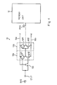
- Fig. 1 shows a typical example of an input circuit 1 incorporated in the dynamic random access memory device, and the input circuit 1 is provided in association with a control signal terminal 2 where a row address strobe signal RAS is applied.
- the input circuit 1 has a first inverting stage 1a implemented by a series combination of a p-channel enhancement type field effect transistor Q1 and an n-channel enhancement type field effect transistor Q2, and the first inverting stage 1a is coupled between an internal power voltage line 3a and a ground line 3b.
- the internal power voltage on the power voltage line 3a is regulated to about 3.3 volts, and an internal row address strobe signal IRAS swings its voltage level between about 3.3 volts and the ground voltage level.
- the internal row address strobe signal IRAS is supplied from the input circuit 1 to a controlling unit 4, and the component field effect transistors of the controlling unit 4 need to withstand 3.3 volts.
- the internal power voltage is produced from an external power voltage level of 5 volts by a built-in step-down circuit 5, and the external power voltage is allowed to fluctuate within 10 %. For this reason, the component field effect transistors of the built-in step-down circuit 5 well withstands 5.5 volts.
- a selected word line is boosted to 5.5 volts, and the boosted word line allows switching field effect transistors to propagate the voltage level on the associated bit lines to storage capacitors without voltage decay. Therefore, the switching transistors of the memory cells are expected to withstand 5.5 volts.
- a semiconductor memory device according to figure 1 is disclosed in US-A-4 984 202.
- the component field effect transistors of input circuits need to withstand the over-shoots, and, for this reason, the input circuits are adapted to withstand 6.5 volts.
- the n-channel enhancement type field effect transistor Q1 has a gate oxide film thick enough to withstand 6.5 volts.
- the component field effect transistors of the 16 megabit dynamic random access memory device operate under various voltage level, and the gate oxide films different in thickness make the process sequence complex. If all of the component field effect transistors are designed to withstand the maximum voltage level of 6.5 volts, the process sequence will become simple. However, the gate oxide films thick enough to withstand 6.5 volts enlarge the component field effect transistors, and the integration density is decreased rather than that produced through the complex process sequence. Thus, there is a trade-off between the Miniaturization of the component field effect transistors and the complexity of the process sequence in the prior art ultra large scaled integration.
- the present invention proposes to cause an external signal to step down before reaching an associated input circuit.
- a semiconductor memory device fabricated on a single semiconductor chip, comprising: a) a plurality of input terminals applied with external signals of a first voltage level; b) external signal input means supplied with the external signals and producing internal signals; c) a memory cell array supplied with the internal signals and other internal signals, and memorizing pieces of data information, the memory cell array being operative to produce a read-out data signal; d) a step-down circuit supplied with an external power voltage and producing an internal power voltage smaller in magnitude than the external power voltage; e) a first voltage line supplied with the internal power voltage; and f) a second voltage line supplied with a constant voltage level different from the internal power voltage, the external signal input means comprising b-1) a logic gate coupled between the first and second voltage lines and responsive to one of the external signals supplied to an input node thereof for producing one of the internal signals of a second voltage level smaller in magnitude than the first voltage level, and b-2) a first field effect transistor coupled between one of the plurality of input terminals applied with external signals of
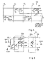
- a dynamic random access memory device embodying the present invention is fabricated on a single semiconductor chip 11, and largely comprises a memory unit 12, input circuits 13, output circuits 14 and a step-down circuit 15.
- the memory unit 12 is further supported by other peripheral circuits and units, they are not illustrated in Fig. 2, because they do not directly concern the gist of the present invention.
- the memory unit 12 has a memory cell array 12a associated with addressing units, data amplifiers and so forth which are controlled by a timing generator.
- the memory cell array 12a is implemented by a plurality of memory cells arranged in rows and columns, and four of the plurality of memory cells are labeled with MC1, MC2, MC3 and MC4 in Fig. 3.
- Each of the memory cells MC1 to MC4 is formed by a series combination of a transfer transistor TR and a storage capacitor CP coupled between an associated bit line BL and a reference voltage line RF, and word lines W1 and W2 are coupled with the gate electrodes of the transfer transistors TR in the associated rows.
- the row addressing unit (not shown) selectively lifts the word lines W1 and W2 to about 5.5 volts, and the transfer transistors TR coupled therewith turn on to conduct the associated bit lines BL to the storage capacitors CP.
- a data bit in the form of either high or low voltage level is written from the associated bit lines BL to the storage capacitors CP, and is read out from the storage capacitor CP to the associated bit line BL.
- the dynamic random access memory device shown in Fig. 2 is operable in a nibble mode, and, accordingly, data bits are transferred from the memory unit 12 through the output circuits 14 to output data terminals OUT1 to OUTn.
- the data write-in sequence and the data read-out sequence are controlled by the timing generator (not shown), and external controlling signals such as a row address strobe signal RAS and a column address strobe signal CAS are supplied from the outside to controlling terminals CTL1 to CTL2, and the input circuits 13 are respectively provided in association with the controlling terminals CTL1 to CTL2.
- the input circuits 13 are responsive to the external controlling signals, and produces internal controlling signals.
- the external controlling signals swing their voltage levels between the ground voltage level and about 5 volts, and over-shoots may take place in the waveforms of the external controlling signals.
- the internal controlling signals swing their voltage levels to a predetermined voltage level lower than 5 volts, because the gate oxide films of most of the component field effect transistors are extremely thin.
- an external power voltage level Vcc of 5 volts steps down at the built-in step-down circuit 15, and an internal power voltage of about 3.3 volts is distributed through an internal power voltage line 15a to the input circuits 13, the memory unit 12 and the output circuits 14.
- the ground voltage level is supplied from a ground terminal GND through a ground voltage line 15b to the input circuits 13, the memory unit 12 and the output circuits 14.
- the output data signals swing their voltage levels between 5 volts and the ground voltage level, and, for this reason, the external power voltage Vcc is directly supplied to the output circuits 14.
- each input circuit 13 is illustrated in Fig. 4, and the input circuit 13 shown in Fig. 4 is assumed to be coupled with the controlling terminal CTL1 for the row address strobe signal RAS.
- the input circuit 13 comprises a plurality of inverting circuits 13a and 13b coupled in cascade, and a step-down transistor 13c coupled between the controlling terminal CTL1 and the first stage of the cascade combination of the inverting circuits 13a and 13b.
- the inverting circuit 13a serves as a logic gate
- the step-down transistor 13c serves as a first field effect transistor.
- Each of the inverting circuits 13a and 13b is implemented by a series combination of a p-channel enhancement type field effect transistor Q11 and an n-channel enhancement type field effect transistor Q12 coupled between the internal power voltage line 15a and the ground voltage line 15b, and the step-down transistor 13c is a n-channel enhancement type field effect transistor.
- the step-down transistor 13c provides a conductive channel between the controlling terminal CTL1 and the gate electrode of the n-channel enhancement type field effect transistor Q12 of the inverting circuit 13a, and the gate electrode of the step-down transistor 13c is coupled with the internal power voltage line 15a.
- the controlling terminal CTL1 is directly coupled with the gate electrode of the p-channel enhancement type field effect transistor Q11 of the inverting circuit 13a, and the output node of each inverting circuit is coupled with the input node of the subsequent stage.
- the input circuit 13 thus arranged is responsive to the row address strobe signal RAS, and produces an internal row address strobe signal IRAS swinging its voltage level between 3.3 volts and the ground voltage level. Since the threshold level of the step-down transistor 13c is regulated to a predetermined value ranging from 0.5 volt to 1.5 volts, a step-down voltage level ranging between 2.3 volts and 2.8 volts is applied to the gate electrode of the n-channel enhancement type field effect transistor Q12.
- the source node of the n-channel enhancement type field effect transistor Q12 is coupled with the ground voltage line 15b, only the step-down voltage level is applied thereto, and the extremely thin gate oxide film is hardly damaged by an over-shoot produced in the row address strobe signal RAS.
- an input circuit 23 incorporated in another dynamic random access memory device embodying the present invention comprises a NOR gate 23a followed by an inverting circuit 23b, and the NOR gate 23a has a series combination of p-channel enhancement type field effect transistors Q21 and Q22, an output node N21 and an n-channel enhancement type field effect transistor Q24 coupled between the internal power voltage line 15a and the ground voltage line 15b, and an n-channel enhancement type field effect transistor Q23 coupled between the output node N21 and the ground voltage line 15b.
- the input circuit 23 is one of a plurality of input circuits corresponding to the input circuits 13, and other component circuits and units are similar to those of the first embodiment.
- the controlling terminal CTL1 is directly coupled with the gate electrode of the p-channel enhancement type field effect transistor Q21 and with the gate electrode of the n-channel enhancement type field effect transistor Q23 through a step-down transistor 23c implemented by an n-channel enhancement type field effect transistor.
- An enable signal ENB is supplied to the gate electrode of the p-channel enhancement type field effect transistor Q22 and the gate electrode of the n-channel enhancement type field effect transistor Q24. Since the step-down transistor 23c decreases the voltage level of the row address strobe signal RAS, the gate oxide film of the n-channel enhancement type field effect transistor is hardly damaged.
- the step-down transistor decreases the voltage level of the row address strobe signal RAS, and the gate oxide film of the n-channel enhancement type field effect transistor is as thin as those of the component field effect transistors applied with the internal power voltage.
- the input circuits can be fabricated from the p-channel enhancement type field effect transistors and only one kind of the n-channel enhancement type field effect transistors.
- the field effect transistors with extremely thin gate oxide films allows decreasing the transistor size, and the integration density is surely improved.
- the present invention is applicable to another type of semiconductor memory device operable with internal signals lower than an external power voltage.
- the step-down transistors may be provided for all of the input circuits or selectively coupled with the input circuits.
Landscapes
- Engineering & Computer Science (AREA)
- Microelectronics & Electronic Packaging (AREA)
- Computer Hardware Design (AREA)
- Dram (AREA)
- Static Random-Access Memory (AREA)
Claims (3)
- Dispositif de mémoire à semi-conducteurs fabriqué sur une puce unique à semi-conducteurs (11), comprenant :a) une pluralité de bornes d'entrée (CTL1 à CTL2) alimentées en signaux externes (RAS/CAS) d'un premier niveau de tension;b) des moyens d'entrée de signaux externes (13/23) alimentés par lesdits signaux externes et produisant des signaux internes;c) un ensemble de cellules de mémoire (MC1 à MC4) alimentées par lesdits signaux internes et en d'autres signaux internes, et des pièces de mémorisation d'informations de données, ledit ensemble de cellules de mémoire étant opérationnel pour produire un signal de données extraites;d) un circuit abaisseur (15) alimenté par une tension électrique externe et produisant une tension électrique interne dont la valeur est inférieure à celle de la tension électrique externe;e) une première ligne de tension (15a) alimentée par ladite tension électrique interne; etf) une deuxième ligne de tension (15b) alimentée par un niveau de tension constant différent de ladite tension électrique interne, lesdits moyens d'entrée de signaux externes comprenantcaractérisé par
b-1) une porte logique (13a/23a) couplée entre lesdites première et deuxième lignes de tension et réagissant à l'un desdits signaux externes pour produire l'un desdits signaux internes d'un deuxième niveau de tension dont la valeur est inférieure audit premier niveau de tension, et
b-2) un premier transistor à effet de champ (13c/23c) couplé entre une borne de ladite pluralité de bornes d'entrée (CTL1) et un noeud d'entrée de ladite porte logique, et ayant une électrode de porte couplée à ladite première ligne de tension de façon à fournir à ladite porte logique un dit signal dudit signal externe de valeur réduite. - Dispositif de mémoire à semi-conducteurs selon la revendication 1, dans lequel ladite porte logique est mise en oeuvre par une combinaison en série (13a) d'un transistor à effet de champ (Q11) du type à enrichissement à canal p et d'un transistor à effet de champ (Q12) du type à enrichissement à canal n, et dans lequel ledit premier transistor à effet de champ fournit un canal conducteur entre ladite borne desdites bornes d'entrée et l'électrode de porte dudit transistor à effet de champ du type à enrichissement à canal n.
- Dispositif de mémoire à semi-conducteurs selon la revendication 1, dans lequel ladite porte logique est mise en oeuvre par une porte NI (23a) ayant des transistors à effet de champ (Q23/Q24) du type à enrichissement à canal n, et dans lequel ledit premier transistor à effet de champ est couplé entre ladite borne desdites bornes d'entrée et l'électrode de porte desdits transistors à effet de champ (Q23) du type à enrichissement à canal n.
Applications Claiming Priority (2)
| Application Number | Priority Date | Filing Date | Title |
|---|---|---|---|
| JP243085/90 | 1990-09-13 | ||
| JP2243085A JPH04123388A (ja) | 1990-09-13 | 1990-09-13 | 半導体メモリ装置 |
Publications (3)
| Publication Number | Publication Date |
|---|---|
| EP0475448A2 EP0475448A2 (fr) | 1992-03-18 |
| EP0475448A3 EP0475448A3 (en) | 1992-10-14 |
| EP0475448B1 true EP0475448B1 (fr) | 1996-08-28 |
Family
ID=17098561
Family Applications (1)
| Application Number | Title | Priority Date | Filing Date |
|---|---|---|---|
| EP91115593A Expired - Lifetime EP0475448B1 (fr) | 1990-09-13 | 1991-09-13 | Dispositif de mémoire à semi-conducteurs ayant un transistor de rabattement pour signal externe |
Country Status (5)
| Country | Link |
|---|---|
| US (1) | US5285412A (fr) |
| EP (1) | EP0475448B1 (fr) |
| JP (1) | JPH04123388A (fr) |
| KR (1) | KR950006420B1 (fr) |
| DE (1) | DE69121657T2 (fr) |
Families Citing this family (2)
| Publication number | Priority date | Publication date | Assignee | Title |
|---|---|---|---|---|
| US5757712A (en) * | 1996-07-12 | 1998-05-26 | International Business Machines Corporation | Memory modules with voltage regulation and level translation |
| JP3804633B2 (ja) * | 2003-05-28 | 2006-08-02 | セイコーエプソン株式会社 | 半導体集積回路 |
Family Cites Families (9)
| Publication number | Priority date | Publication date | Assignee | Title |
|---|---|---|---|---|
| US4216390A (en) * | 1978-10-04 | 1980-08-05 | Rca Corporation | Level shift circuit |
| US4482985A (en) * | 1981-04-17 | 1984-11-13 | Hitachi, Ltd. | Semiconductor integrated circuit |
| JPS5990292A (ja) * | 1982-11-12 | 1984-05-24 | Toshiba Corp | 電圧変換回路 |
| JPS6052112A (ja) * | 1983-08-31 | 1985-03-25 | Toshiba Corp | 論理回路 |
| NL8702800A (nl) * | 1987-11-23 | 1989-06-16 | Philips Nv | Geintegreerde geheugenschakeling met interne voedingsspanningsregeling. |
| US4820941A (en) * | 1988-02-01 | 1989-04-11 | Texas Instruments Incorporated | Decoder driver circuit for programming high-capacitance lines |
| JP2585348B2 (ja) * | 1988-02-22 | 1997-02-26 | 株式会社東芝 | 不揮発性半導体記憶装置 |
| JPH02246516A (ja) * | 1989-03-20 | 1990-10-02 | Hitachi Ltd | 半導体装置 |
| US5084637A (en) * | 1989-05-30 | 1992-01-28 | International Business Machines Corp. | Bidirectional level shifting interface circuit |
-
1990
- 1990-09-13 JP JP2243085A patent/JPH04123388A/ja active Pending
-
1991
- 1991-09-10 KR KR1019910015759A patent/KR950006420B1/ko not_active Expired - Lifetime
- 1991-09-13 EP EP91115593A patent/EP0475448B1/fr not_active Expired - Lifetime
- 1991-09-13 US US07/759,294 patent/US5285412A/en not_active Expired - Lifetime
- 1991-09-13 DE DE69121657T patent/DE69121657T2/de not_active Expired - Lifetime
Also Published As
| Publication number | Publication date |
|---|---|
| JPH04123388A (ja) | 1992-04-23 |
| EP0475448A3 (en) | 1992-10-14 |
| DE69121657T2 (de) | 1997-02-06 |
| DE69121657D1 (de) | 1996-10-02 |
| KR920007172A (ko) | 1992-04-28 |
| EP0475448A2 (fr) | 1992-03-18 |
| KR950006420B1 (ko) | 1995-06-15 |
| US5285412A (en) | 1994-02-08 |
Similar Documents
| Publication | Publication Date | Title |
|---|---|---|
| US7372768B2 (en) | Memory with address management | |
| US5532961A (en) | Semiconductor memory device having extended data out function | |
| US5117426A (en) | Circuit, device, and method to detect voltage leakage | |
| US4644501A (en) | Semiconductor memory device with charging circuit | |
| US5410505A (en) | Semiconductor memory device having a memory cell unit including a plurality of transistors connected in series | |
| US6400593B1 (en) | Ternary CAM cell with DRAM mask circuit | |
| US20040004899A1 (en) | Word line driving circuit | |
| US5307314A (en) | Split read/write dynamic random access memory | |
| EP1614118A2 (fr) | Amplificateur de detection a basse tension et procede associe | |
| US5793692A (en) | Integrated circuit memory with back end mode disable | |
| JPS61160898A (ja) | 半導体記憶装置 | |
| US5493536A (en) | Dual-port random access memory having memory cell controlled by write data lines and read enable line | |
| JP2604276B2 (ja) | 半導体記憶装置 | |
| US4876671A (en) | Semiconductor dynamic memory device with metal-level selection of page mode or nibble mode | |
| US5668485A (en) | Row decoder with level translator | |
| US5818751A (en) | Single-port SRAM with no read/write collisions | |
| US6307793B1 (en) | Memory device, coupling noise eliminator, and coupling noise elimination method | |
| US11282569B2 (en) | Apparatus with latch balancing mechanism and methods for operating the same | |
| EP0062547A2 (fr) | Circuit de mémoire | |
| US4870617A (en) | Semiconductor memory device having data bus reset circuits | |
| US5862072A (en) | Memory array architecture and method for dynamic cell plate sensing | |
| US5999461A (en) | Low voltage bootstrapping circuit | |
| US4779230A (en) | CMOS static ram cell provided with an additional bipolar drive transistor | |
| EP0475448B1 (fr) | Dispositif de mémoire à semi-conducteurs ayant un transistor de rabattement pour signal externe | |
| US5245579A (en) | Semiconductor memory device |
Legal Events
| Date | Code | Title | Description |
|---|---|---|---|
| PUAI | Public reference made under article 153(3) epc to a published international application that has entered the european phase |
Free format text: ORIGINAL CODE: 0009012 |
|
| 17P | Request for examination filed |
Effective date: 19910913 |
|
| AK | Designated contracting states |
Kind code of ref document: A2 Designated state(s): DE FR GB |
|
| PUAL | Search report despatched |
Free format text: ORIGINAL CODE: 0009013 |
|
| AK | Designated contracting states |
Kind code of ref document: A3 Designated state(s): DE FR GB |
|
| 17Q | First examination report despatched |
Effective date: 19951019 |
|
| GRAH | Despatch of communication of intention to grant a patent |
Free format text: ORIGINAL CODE: EPIDOS IGRA |
|
| GRAA | (expected) grant |
Free format text: ORIGINAL CODE: 0009210 |
|
| GRAH | Despatch of communication of intention to grant a patent |
Free format text: ORIGINAL CODE: EPIDOS IGRA |
|
| AK | Designated contracting states |
Kind code of ref document: B1 Designated state(s): DE FR GB |
|
| REF | Corresponds to: |
Ref document number: 69121657 Country of ref document: DE Date of ref document: 19961002 |
|
| ET | Fr: translation filed | ||
| PLBE | No opposition filed within time limit |
Free format text: ORIGINAL CODE: 0009261 |
|
| STAA | Information on the status of an ep patent application or granted ep patent |
Free format text: STATUS: NO OPPOSITION FILED WITHIN TIME LIMIT |
|
| 26N | No opposition filed | ||
| REG | Reference to a national code |
Ref country code: GB Ref legal event code: IF02 |
|
| REG | Reference to a national code |
Ref country code: GB Ref legal event code: 732E |
|
| REG | Reference to a national code |
Ref country code: FR Ref legal event code: TQ |
|
| REG | Reference to a national code |
Ref country code: GB Ref legal event code: 732E |
|
| REG | Reference to a national code |
Ref country code: FR Ref legal event code: TP |
|
| PGFP | Annual fee paid to national office [announced via postgrant information from national office to epo] |
Ref country code: GB Payment date: 20090909 Year of fee payment: 19 |
|
| PGFP | Annual fee paid to national office [announced via postgrant information from national office to epo] |
Ref country code: FR Payment date: 20100921 Year of fee payment: 20 |
|
| PGFP | Annual fee paid to national office [announced via postgrant information from national office to epo] |
Ref country code: DE Payment date: 20100908 Year of fee payment: 20 |
|
| GBPC | Gb: european patent ceased through non-payment of renewal fee |
Effective date: 20100913 |
|
| PG25 | Lapsed in a contracting state [announced via postgrant information from national office to epo] |
Ref country code: GB Free format text: LAPSE BECAUSE OF NON-PAYMENT OF DUE FEES Effective date: 20100913 |
|
| REG | Reference to a national code |
Ref country code: DE Ref legal event code: R071 Ref document number: 69121657 Country of ref document: DE |
|
| REG | Reference to a national code |
Ref country code: DE Ref legal event code: R071 Ref document number: 69121657 Country of ref document: DE |
|
| PG25 | Lapsed in a contracting state [announced via postgrant information from national office to epo] |
Ref country code: DE Free format text: LAPSE BECAUSE OF EXPIRATION OF PROTECTION Effective date: 20110914 |