EP0475764A2 - Circuit décodeur redondant - Google Patents
Circuit décodeur redondant Download PDFInfo
- Publication number
- EP0475764A2 EP0475764A2 EP91308344A EP91308344A EP0475764A2 EP 0475764 A2 EP0475764 A2 EP 0475764A2 EP 91308344 A EP91308344 A EP 91308344A EP 91308344 A EP91308344 A EP 91308344A EP 0475764 A2 EP0475764 A2 EP 0475764A2
- Authority
- EP
- European Patent Office
- Prior art keywords
- redundant
- memory cell
- decoder circuit
- signal
- memory
- Prior art date
- Legal status (The legal status is an assumption and is not a legal conclusion. Google has not performed a legal analysis and makes no representation as to the accuracy of the status listed.)
- Granted
Links
- 239000004065 semiconductor Substances 0.000 description 10
- 238000010586 diagram Methods 0.000 description 6
- 230000003068 static effect Effects 0.000 description 2
- 238000010276 construction Methods 0.000 description 1
- 230000004048 modification Effects 0.000 description 1
- 238000012986 modification Methods 0.000 description 1
Images

Classifications
-
- G—PHYSICS
- G11—INFORMATION STORAGE
- G11C—STATIC STORES
- G11C29/00—Checking stores for correct operation ; Subsequent repair; Testing stores during standby or offline operation
-
- G—PHYSICS
- G11—INFORMATION STORAGE
- G11C—STATIC STORES
- G11C29/00—Checking stores for correct operation ; Subsequent repair; Testing stores during standby or offline operation
- G11C29/70—Masking faults in memories by using spares or by reconfiguring
- G11C29/78—Masking faults in memories by using spares or by reconfiguring using programmable devices
- G11C29/785—Masking faults in memories by using spares or by reconfiguring using programmable devices with redundancy programming schemes
- G11C29/787—Masking faults in memories by using spares or by reconfiguring using programmable devices with redundancy programming schemes using a fuse hierarchy
-
- G—PHYSICS
- G11—INFORMATION STORAGE
- G11C—STATIC STORES
- G11C29/00—Checking stores for correct operation ; Subsequent repair; Testing stores during standby or offline operation
- G11C29/70—Masking faults in memories by using spares or by reconfiguring
- G11C29/78—Masking faults in memories by using spares or by reconfiguring using programmable devices
- G11C29/83—Masking faults in memories by using spares or by reconfiguring using programmable devices with reduced power consumption
- G11C29/832—Masking faults in memories by using spares or by reconfiguring using programmable devices with reduced power consumption with disconnection of faulty elements
Definitions
- This invention relates to a redundant decoder circuit employed in a semiconductor memory device.
- a semiconductor memory device includes a redundant memory which stores a predetermined information instead of a main memory when a memory cell of the main memory is disabled, and a redundant decoder circuit supplies an active signal to the redundant memory in accordance with an address signal.
- a conventional redundant decoder circuit includes a plurality of fuses which are cut to correspond to a content of the address signal.
- this redundant decoder circuit when an address signal corresponding to a normal memory cell of the main memory is applied to the redundant decoder circuit, no signal is applied to the redundant memory in accordance with the address signal, so that the redundant memory becomes inactive state.
- an address signal corresponding to a disabled memory cell of the main memory is applied to the redundant decoder circuit, an active signal is applied to the redundant memory to activate a predetermined redundant memory cell.
- the conventional redundant decoder circuit there is a disadvantage in that if a redundant memory cell selected by the redundant decoder circuit is disabled, a semiconductor memory circuit is not used as a whole, even if there is left a normal redundant memory cell in the redundant memory. As the result, the semiconductor memory device must be replaced by another one to lower a fabricating yield.
- a redundant decoder circuit comprises: means for storing an address to designate a memory cell of a main memory which is disabled; means fore generating a first decode signal, when an address signal coincides with the address stored in the storing means; a memory cell of a redundant memory for storing information, when the first decode signal is generated; and means for restoring the generating means to generate a second decode signal which is an inverted signal of the first decode signal.
- a semiconductor memory device includes a main decoder 10 connected to an address signal generating circuit 12, a main memory 14 connected to the main decoder 10, a detector 15 connected to the address signal generating circuit 12, a redundant decoder 16 connected to the detector 15 and a redundant memory 18 connected to the redundant decoder 16.
- the detector 15 and the redundant decoder 16 provide a redundant decoder circuit 19 in combination.
- An address information of disabled memory cells in the main memory 14 is stored in the detector 15, and the detector 15 detects the disabled address.
- the main decoder circuit 10 when an address signal of n-bits is supplied to the main decoder circuit 10 and the detector 15, the main decoder circuit 10 supplies an active signal to the main memory 14 and the detector 15 compares the received address with the stored disabled address. When the received address does not correspond to the disabled address, the main memory 14 stores a predetermined information in a memory cell corresponding to the address. At this time, an active signal is not supplied from the redundant decoder circuit 16 to the redundant memory 18. On the other hand, if the received address corresponds to the disabled address, an active signal is supplied to the redundant memory 18. As the result, the redundant memory 18 stores a predetermined information instead of the main memory 14.
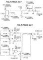
- the first conventional redundant decoder circuit of dynamic type shown in Fig. 2 which corresponds to the redundant decoder circuit 19 of Fig. 1, includes a P-channel transistor 20 connected at a source to a power supply, N-channel transistors N1, N2, ⁇ , Nn each connected at a gate to the address signal generating circuit and at a drain to ground, fuses F1, F2, ⁇ , Fn connected between a common drain of the P-channel transistor 20 connected to a bus line 22 and a corresponding source of the N-channel transistors N1, N2, ⁇ , Nn, two inverters 24 and 26 positioned in series between the bus line 22 and an decode line 30, and a P-channel transistor 31 connected at a source to a power supply at a drain to the bus line 22, and at a gate to an output of the inverter 24.
- the fuse F2 is cut to store an address signal "0
- the redundant decoder circuit which corresponds to the redundant decoder circuit 19 of Fig. 1 includes P-channel transistors P1, P2., ⁇ , Pn each connected at a source to a power supply, fuses F1, F2, ⁇ , Fn respectively connected between a corresponding drain of the P-channel transistors P1, P2, ⁇ , Pn and ground, a P-channel transistor 32 connected at a source to a power supply and at a gate to ground, a fuse 34 connected between a drain of the P-channel transistor 32 and ground, an inverter 36 connected at an input to a node between the P-channel transistor 32 and the fuse 34 and at an output to gates of the P-channel transistors P1, P2, ⁇ , Pn, exclusive NOR gates EX1, EX2, ⁇ , EXn connected at inputs to lines 90 and 91, 92 and 93, and 94 and 95, respectively, a NAND gate 38 connected at inputs
- the lines 90, 92 and 94 are connected to nodes between the P-channel transistor P1 and fuse F1, P2 and F2, and Pn and Fn, respectively.
- Each of the lines 91, 93 and 95 is connected to the address signal generating circuit.
- the fuse F2 is cut, the remaining fuse are not cut.
- the decoder circuit is activated by cutting the fuse 34, so that the P-channel transistors P1, P2, ⁇ , Pn are turned on.
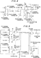
- the redundant decoder circuit of dynamic type includes a P-channel transistor 20 connected at a source to a power supply, N-channel transistors N1, N2, ⁇ , Nn each connected at a gate to the address signal generating circuit and at a drain to ground, fuses F1, F2, ⁇ , Fn connected between a common drain of the P-channel transistor 20 connected to a bus line 22 and a corresponding source of the N-channel transistors N1, N2, ⁇ , Nn, respectively, two inverters 24 and 26 positioned in series between the bus line 22 and an decode line 30, a P-channel transistor 31 connected at a source to a power supply at a drain to the bus line 22, and at a gate to an output of the inverter 24, and a restoration circuit 200.
- the fuse F2 is cut to store an address signal "0, ⁇ , 1, 0".
- the restoration circuit consists of an N-channel transistor 50 connected at a source to a bus line 22 and at a drain to ground, a P-channel transistor 52 connected at a source to a power supply and at a gate to ground, and a fuse 54 connected between a drain of the P-channel transistor 52 and ground.
- the N-channel transistor 50 is connected at a gate to a node 110 between the drain of the P-channel transistor 52 and the fuse 54.
- the fuse 54 is disconnected in the restoration circuit 200. Then, a signal of level "1" is applied to the gate of the N-channel transistor 50 through the node 110, so that a level of the bus line 22 becomes “0", and a level of the decode line 30 becomes “0", as shown in the table by No. 3. Therefore, the addressed memory cell of the redundant memory becomes inactive state.
- the predetermined information is to be stored in another memory cell of the redundant memory instead of the disabled memory cell thereof by cutting a fuse corresponding to the fuse F2.
- the redundant decoder circuit includes P-channel transistors P1, P2, ⁇ , Pn each connected at a source to a power supply, fuses F1, F2, ⁇ , Fn respectively connected between a corresponding drain of the P-channel transistors P1, P2, ⁇ , Pn and ground, a P-channel transistor 32 connected at a source to a power supply and at a gate to ground, a fuse 34 connected between a drain of the P-channel transistor 32 and ground, an inverter 36 connected at an input to a node between the P-channel transistor 32 and the fuse 34 and at an output to gates of the P-channel transistors P1, P2, ⁇ , Pn, exclusive NOR gates EX1, EX2, ⁇ , EXn connected at inputs to lines 90 and 91, 92 and 93, and 94 and 95, respectively, a NAND gate 38 connected at inputs to outputs of the exclusive NOR gates
- the lines 90, 92 and 94 are connected to nodes between the P-channel transistor P1 and fuse F1, P2 and F2, and Pn and Fn, respectively.
- Each of the lines 91, 93 and 95 is connected to the address signal generating circuit.
- the restoration circuit 200 consists of an N-channel transistor 60 connected at a drain to ground and at a gate to a power supply, and a fuse 62 connected between a power supply and a source of the N-channel transistor 60.
- a node 96 between the N-channel transistor 60 and the fuse 62 is connected to one of inputs of the NAND gate 38.
- the decoder circuit is activated by cutting the fuse 34, so that the P-channel transistors P1, P2, ⁇ , Pn are turned on.
- the fuse 62 is disconnected.
- a level of the node 96 becomes “0”, so that a signal of level "0” is applied to one of inputs of the NAND gate 38. Therefore, a level of the output line 39 becomes “0", so that the addressed memory cell of the redundant memory becomes inactive state as shown in the table by No. 3.
- the predetermined information is to be stored in another memory cell of the redundant memory instead of the disabled memory cell thereof by cutting a fuse corresponding to the fuse F2.
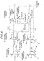
- the redundant decoder circuit includes a first and second decoder circuits and a control circuit 70 connected between the first and second decoder circuits.
- the first decoder circuit includes a P-channel transistor 20 connected at a source to a power supply, N-channel transistors N1, N2, ⁇ , Nn each connected at a gate to the address signal generating circuit and at a drain to ground, fuses F1, F2, ⁇ , Fn connected between a common drain of the P-channel transistor 20 connected to a bus line 22 and a corresponding source of the N-channel transistors N1, N2, ⁇ , Nn, respectively, an inverter 24, and a P-channel transistor 31 connected at a source to a power supply.
- the second decoder circuit has the same structure as the first decoder circuit.
- a P-channel transistor 120 corresponds to the transistor 20
- fuses B1, B2 and Bn corresponds respectively to the fuses F1, F2 and Fn
- N-channel transistors A1, A2 and An correspond respectively to the N-channel transistors N1, N2 and Nn
- a P-channel transistor 131 corresponds to the transistor 31
- an inverter 124 corresponds to the inverter 24.
- the control circuit 70 includes an inverter 72 connected at an input to an output of the first decoder circuit, a NOR gate 74 connected at one of inputs to the output of the first decoder circuit through a node 300 and at an output to a first decode line 76, a NAND gate 78 connected at one of inputs to an output of the inverter 72, a NAND gate 80 connected at inputs to outputs of the NAND gate 78 and the inverter 124 through a line 310 and at an output to a second decode line 82, a P-channel transistor 84 connected at a source to a power supply and at a gate to ground, and a fuse 86 connected between ground and a drain of the P-channel transistor 84 through a node 220.
- a level of the first decode line 76 becomes "0", so that a memory cell of the redundant memory which is to be accessed by the first decode line 76 becomes inactive state.
- the first and second decoder circuits may decode first and second address signal, respectively, to enable the first and second decode lines 76 and 82, so that an information is written into two corresponding redundant memory cells in place of two disabled main memory cells, when the first and second address signals coincide with stored address signals determined by the cut patterns of the fuse F1, F2, ⁇ , Fn and the fuse B1, B2, ⁇ , Bn of the first and second decoder circuits.
Landscapes
- For Increasing The Reliability Of Semiconductor Memories (AREA)
- Dram (AREA)
- Static Random-Access Memory (AREA)
Applications Claiming Priority (2)
| Application Number | Priority Date | Filing Date | Title |
|---|---|---|---|
| JP243086/90 | 1990-09-13 | ||
| JP2243086A JP2778234B2 (ja) | 1990-09-13 | 1990-09-13 | 冗長デコーダ回路 |
Publications (3)
| Publication Number | Publication Date |
|---|---|
| EP0475764A2 true EP0475764A2 (fr) | 1992-03-18 |
| EP0475764A3 EP0475764A3 (en) | 1993-03-17 |
| EP0475764B1 EP0475764B1 (fr) | 1996-05-01 |
Family
ID=17098578
Family Applications (1)
| Application Number | Title | Priority Date | Filing Date |
|---|---|---|---|
| EP91308344A Expired - Lifetime EP0475764B1 (fr) | 1990-09-13 | 1991-09-12 | Circuit décodeur redondant |
Country Status (5)
| Country | Link |
|---|---|
| US (1) | US5311472A (fr) |
| EP (1) | EP0475764B1 (fr) |
| JP (1) | JP2778234B2 (fr) |
| KR (1) | KR960005361B1 (fr) |
| DE (1) | DE69119170T2 (fr) |
Cited By (1)
| Publication number | Priority date | Publication date | Assignee | Title |
|---|---|---|---|---|
| FR2718560A1 (fr) * | 1994-04-11 | 1995-10-13 | Samsung Electronics Co Ltd | Procédé et circuit pour réparer un défaut dans un dispositif de mémoire à semi-conducteur. |
Families Citing this family (17)
| Publication number | Priority date | Publication date | Assignee | Title |
|---|---|---|---|---|
| JPH04192198A (ja) * | 1990-11-27 | 1992-07-10 | Mitsubishi Electric Corp | 冗長回路 |
| US5550776A (en) * | 1994-04-06 | 1996-08-27 | Samsung Electronics Co., Ltd. | Semiconductor memory device capable of driving word lines at high speed |
| EP0646866A3 (fr) * | 1993-09-30 | 1998-05-27 | STMicroelectronics, Inc. | Validation-maítre pour décodeur de rangée redondante |
| US5548225A (en) * | 1994-05-26 | 1996-08-20 | Texas Instruments Incorportated | Block specific spare circuit |
| JPH08111098A (ja) * | 1994-10-12 | 1996-04-30 | Nec Corp | メモリ回路 |
| JPH08212797A (ja) * | 1995-01-31 | 1996-08-20 | Nec Corp | 半導体装置 |
| KR0157344B1 (ko) * | 1995-05-25 | 1998-12-01 | 김광호 | 반도체 메모리 장치의 퓨즈소자 회로 |
| US5612918A (en) * | 1995-12-29 | 1997-03-18 | Sgs-Thomson Microelectronics, Inc. | Redundancy architecture |
| US5841709A (en) * | 1995-12-29 | 1998-11-24 | Stmicroelectronics, Inc. | Memory having and method for testing redundant memory cells |
| US6037799A (en) * | 1995-12-29 | 2000-03-14 | Stmicroelectronics, Inc. | Circuit and method for selecting a signal |
| US5771195A (en) * | 1995-12-29 | 1998-06-23 | Sgs-Thomson Microelectronics, Inc. | Circuit and method for replacing a defective memory cell with a redundant memory cell |
| JPH10123202A (ja) * | 1996-10-21 | 1998-05-15 | Nec Ic Microcomput Syst Ltd | 半導体集積回路装置 |
| US5886940A (en) * | 1997-08-21 | 1999-03-23 | Micron Technology, Inc. | Self-protected circuit for non-selected programmable elements during programming |
| US6868019B2 (en) * | 2003-07-02 | 2005-03-15 | Micron Technology, Inc. | Reduced power redundancy address decoder and comparison circuit |
| US7915916B2 (en) * | 2006-06-01 | 2011-03-29 | Micron Technology, Inc. | Antifuse programming circuit with snapback select transistor |
| US7489180B2 (en) * | 2006-07-28 | 2009-02-10 | Texas Instruments Incorporated | Systems and methods for efuse fusing time reduction |
| JP5650366B2 (ja) * | 2007-10-29 | 2015-01-07 | ピーエスフォー ルクスコ エスエイアールエルPS4 Luxco S.a.r.l. | アンチヒューズ回路及びこれを備える半導体装置、並びに、アンチヒューズ回路へのアドレス書き込み方法 |
Family Cites Families (5)
| Publication number | Priority date | Publication date | Assignee | Title |
|---|---|---|---|---|
| US4577294A (en) * | 1983-04-18 | 1986-03-18 | Advanced Micro Devices, Inc. | Redundant memory circuit and method of programming and verifying the circuit |
| JPH0235699A (ja) * | 1988-07-26 | 1990-02-06 | Nec Corp | 化合物半導体メモリデバイス |
| JPH02116098A (ja) * | 1988-10-24 | 1990-04-27 | Nec Corp | 冗長回路を有する半導体メモリ |
| JPH02310898A (ja) * | 1989-05-25 | 1990-12-26 | Nec Corp | メモリ回路 |
| JPH03104097A (ja) * | 1989-09-18 | 1991-05-01 | Fujitsu Ltd | 半導体記憶装置 |
-
1990
- 1990-09-13 JP JP2243086A patent/JP2778234B2/ja not_active Expired - Lifetime
-
1991
- 1991-09-12 DE DE69119170T patent/DE69119170T2/de not_active Expired - Lifetime
- 1991-09-12 EP EP91308344A patent/EP0475764B1/fr not_active Expired - Lifetime
- 1991-09-12 KR KR1019910015920A patent/KR960005361B1/ko not_active Expired - Lifetime
- 1991-09-13 US US07/759,289 patent/US5311472A/en not_active Expired - Lifetime
Cited By (1)
| Publication number | Priority date | Publication date | Assignee | Title |
|---|---|---|---|---|
| FR2718560A1 (fr) * | 1994-04-11 | 1995-10-13 | Samsung Electronics Co Ltd | Procédé et circuit pour réparer un défaut dans un dispositif de mémoire à semi-conducteur. |
Also Published As
| Publication number | Publication date |
|---|---|
| DE69119170T2 (de) | 1997-01-02 |
| KR960005361B1 (ko) | 1996-04-24 |
| JPH04123399A (ja) | 1992-04-23 |
| US5311472A (en) | 1994-05-10 |
| JP2778234B2 (ja) | 1998-07-23 |
| EP0475764B1 (fr) | 1996-05-01 |
| KR920006995A (ko) | 1992-04-28 |
| DE69119170D1 (de) | 1996-06-05 |
| EP0475764A3 (en) | 1993-03-17 |
Similar Documents
| Publication | Publication Date | Title |
|---|---|---|
| US5311472A (en) | Redundant decoder circuit | |
| US4714839A (en) | Control circuit for disabling or enabling the provision of redundancy | |
| US5349243A (en) | Latch controlled output driver | |
| JPH0877791A (ja) | 半導体メモリ装置のカラム冗長方法及びその回路 | |
| US4614881A (en) | Integrated semiconductor circuit device for generating a switching control signal using a flip-flop circuit including CMOS FET's and flip-flop setting means | |
| EP0376245A2 (fr) | Dispositif de mémoire à semi-conducteurs muni d'un décodeur redondant | |
| EP1288967A2 (fr) | Mémoire à semiconducteurs | |
| JPH0778994B2 (ja) | 半導体記憶装置 | |
| US5257228A (en) | Efficiency improved DRAM row redundancy circuit | |
| KR100302424B1 (ko) | 논리하이브리드메모리용반도체메모리 | |
| US5293561A (en) | Write-in voltage source incorporated in electrically erasable programmable read only memory device with redundant memory cell array | |
| US5892711A (en) | Sector protection circuit for a flash memory device | |
| KR19990011067A (ko) | 리던던시 회로 및 이를 구비하는 반도체장치 | |
| KR100361656B1 (ko) | 반도체 메모리 장치의 고전압 발생회로 | |
| US5801457A (en) | Unit for maintaining information regarding the state of a device during battery power | |
| JP2973419B2 (ja) | 半導体メモリ装置 | |
| JP2894556B2 (ja) | 半導体記憶装置 | |
| US6862231B2 (en) | Repair circuit | |
| KR100224763B1 (ko) | 반도체 메모리 장치의 전원전압 공급회로 | |
| KR100197988B1 (ko) | 반도체 메모리 장치의 리던던시 회로 | |
| KR100311216B1 (ko) | 스탠바이 전류의 흐름을 차단시키기 위한 메모리 소자의 리페어 회로 | |
| KR950003395B1 (ko) | 어드레스 핀을 이용한 상태 제어장치 | |
| KR100378336B1 (ko) | 반도체장치의기억회로 | |
| KR20010029312A (ko) | 리던던시 제어회로 | |
| KR20010041910A (ko) | 전력소모를 최소화하기 위하여 미사용 컨피그레이션비트를 파워다운하는 회로 |
Legal Events
| Date | Code | Title | Description |
|---|---|---|---|
| PUAI | Public reference made under article 153(3) epc to a published international application that has entered the european phase |
Free format text: ORIGINAL CODE: 0009012 |
|
| 17P | Request for examination filed |
Effective date: 19911001 |
|
| AK | Designated contracting states |
Kind code of ref document: A2 Designated state(s): DE FR GB |
|
| PUAL | Search report despatched |
Free format text: ORIGINAL CODE: 0009013 |
|
| AK | Designated contracting states |
Kind code of ref document: A3 Designated state(s): DE FR GB |
|
| 17Q | First examination report despatched |
Effective date: 19950929 |
|
| GRAH | Despatch of communication of intention to grant a patent |
Free format text: ORIGINAL CODE: EPIDOS IGRA |
|
| GRAA | (expected) grant |
Free format text: ORIGINAL CODE: 0009210 |
|
| AK | Designated contracting states |
Kind code of ref document: B1 Designated state(s): DE FR GB |
|
| REF | Corresponds to: |
Ref document number: 69119170 Country of ref document: DE Date of ref document: 19960605 |
|
| ET | Fr: translation filed | ||
| PLBE | No opposition filed within time limit |
Free format text: ORIGINAL CODE: 0009261 |
|
| STAA | Information on the status of an ep patent application or granted ep patent |
Free format text: STATUS: NO OPPOSITION FILED WITHIN TIME LIMIT |
|
| 26N | No opposition filed | ||
| REG | Reference to a national code |
Ref country code: GB Ref legal event code: IF02 |
|
| REG | Reference to a national code |
Ref country code: GB Ref legal event code: 732E |
|
| REG | Reference to a national code |
Ref country code: FR Ref legal event code: TQ |
|
| REG | Reference to a national code |
Ref country code: GB Ref legal event code: 732E |
|
| REG | Reference to a national code |
Ref country code: FR Ref legal event code: TP |
|
| PGFP | Annual fee paid to national office [announced via postgrant information from national office to epo] |
Ref country code: GB Payment date: 20090909 Year of fee payment: 19 |
|
| PGFP | Annual fee paid to national office [announced via postgrant information from national office to epo] |
Ref country code: FR Payment date: 20100921 Year of fee payment: 20 |
|
| PGFP | Annual fee paid to national office [announced via postgrant information from national office to epo] |
Ref country code: DE Payment date: 20100908 Year of fee payment: 20 |
|
| GBPC | Gb: european patent ceased through non-payment of renewal fee |
Effective date: 20100912 |
|
| PG25 | Lapsed in a contracting state [announced via postgrant information from national office to epo] |
Ref country code: GB Free format text: LAPSE BECAUSE OF NON-PAYMENT OF DUE FEES Effective date: 20100912 |
|
| REG | Reference to a national code |
Ref country code: DE Ref legal event code: R071 Ref document number: 69119170 Country of ref document: DE |
|
| REG | Reference to a national code |
Ref country code: DE Ref legal event code: R071 Ref document number: 69119170 Country of ref document: DE |
|
| PG25 | Lapsed in a contracting state [announced via postgrant information from national office to epo] |
Ref country code: DE Free format text: LAPSE BECAUSE OF EXPIRATION OF PROTECTION Effective date: 20110913 |