EP0476581A1 - Vorrichtung zur Erzeugung eines mit der Phase der Leistungsversorgung synchronisierten digitalen Signals - Google Patents
Vorrichtung zur Erzeugung eines mit der Phase der Leistungsversorgung synchronisierten digitalen Signals Download PDFInfo
- Publication number
- EP0476581A1 EP0476581A1 EP91115743A EP91115743A EP0476581A1 EP 0476581 A1 EP0476581 A1 EP 0476581A1 EP 91115743 A EP91115743 A EP 91115743A EP 91115743 A EP91115743 A EP 91115743A EP 0476581 A1 EP0476581 A1 EP 0476581A1
- Authority
- EP
- European Patent Office
- Prior art keywords
- phase
- value
- signal
- difference angle
- signals
- Prior art date
- Legal status (The legal status is an assumption and is not a legal conclusion. Google has not performed a legal analysis and makes no representation as to the accuracy of the status listed.)
- Granted
Links
Images


Classifications
-
- H—ELECTRICITY
- H02—GENERATION; CONVERSION OR DISTRIBUTION OF ELECTRIC POWER
- H02M—APPARATUS FOR CONVERSION BETWEEN AC AND AC, BETWEEN AC AND DC, OR BETWEEN DC AND DC, AND FOR USE WITH MAINS OR SIMILAR POWER SUPPLY SYSTEMS; CONVERSION OF DC OR AC INPUT POWER INTO SURGE OUTPUT POWER; CONTROL OR REGULATION THEREOF
- H02M1/00—Details of apparatus for conversion
- H02M1/08—Circuits specially adapted for the generation of control voltages for semiconductor devices incorporated in static converters
- H02M1/081—Circuits specially adapted for the generation of control voltages for semiconductor devices incorporated in static converters wherein the phase of the control voltage is adjustable with reference to the AC source
- H02M1/082—Circuits specially adapted for the generation of control voltages for semiconductor devices incorporated in static converters wherein the phase of the control voltage is adjustable with reference to the AC source with digital control
-
- H—ELECTRICITY
- H03—ELECTRONIC CIRCUITRY
- H03L—AUTOMATIC CONTROL, STARTING, SYNCHRONISATION OR STABILISATION OF GENERATORS OF ELECTRONIC OSCILLATIONS OR PULSES
- H03L7/00—Automatic control of frequency or phase; Synchronisation
- H03L7/06—Automatic control of frequency or phase; Synchronisation using a reference signal applied to a frequency- or phase-locked loop
- H03L7/08—Details of the phase-locked loop
- H03L7/085—Details of the phase-locked loop concerning mainly the frequency- or phase-detection arrangement including the filtering or amplification of its output signal
- H03L7/091—Details of the phase-locked loop concerning mainly the frequency- or phase-detection arrangement including the filtering or amplification of its output signal the phase or frequency detector using a sampling device
Definitions
- the present invention relates to an apparatus for feeding a digital signal synchronized with a phase of an a.c. power supply.
- a control system for those systems requires a signal synchronized with a phase of the d.c. power supply so that the control system works in synchronization with the phase of an a.c. power supply.
- microcomputers have been widely used in phase control units of thyristors as well as other control units.
- Fig. 1 shows an arrangement of a representative phase locked loop circuit.
- a voltage detector 1 steps down a supply voltage and outputs phase voltage signals U, V, W to a logic detector circuit 2.
- the logic detector circuit 2 serves to transform the voltage signals U, V, W into a logic level “1” or “0” depending on the polarity of each signal and to feed logic signals 2a to 2c to a ROM 3 in which those logic signals 2a to 2c are applied, to lower rank addresses A0 to A2 of the ROM 2.
- the upper rank addresses A3 to A6 of the ROM 3 receive frequency-divided signals 7a to 7d sent from a frequency divider circuit 7.
- the ROM 3 stores pieces of binary voltage information 3a to 3c at the addresses corresponding to those address signals.
- Each binary voltage information 3a to 3c is read from a data output terminal D0 to D2 of the ROM 3 and is added to an adder 4.
- the ROM 3 has the other data output terminal D3 from which a frequency-division clearing signal 3d is read, and is added to the frequency dividing circuit 7. This clearing signal 3d serves to limit the division of an electric angle 180° into 12 partial frequencies.
- the adder 4 serves to add the corresponding voltage signal to each binary voltage information 3a to 3c and add the added signal 4a to a voltage smoothing circuit 5.
- the voltage smoothing circuit 5 serves to smooth the added signal 4a and feed a smoothed voltage signal 5a to a voltage oscillation circuit 6.
- the voltage oscillation circuit 6 transforms the smoothed voltage signal 5a into the corresponding pulse frequency signal 6a, for example, a frequency corresponding to 12-fold power frequency f s .
- the frequency divider circuit 7 divides the pulse signal 6a into divided frequency signals 7a to 7d of 1/16, 1/8, 1/4 and 1/2.
- the ROM 3 specifies each binary data stored at each phase interval 15° (180°/120 to the corresponding address so that the ROM 3 may output a voltage signal 3a of "1" at a first 90° interval (0 to 90°), a signal 3a of "0” at a second 90° interval (90° to 180°), a signal 3a of "1” at a third 90° interval (180° to 270°), and a signal 3a of "0” at a fourth 90° interval (270° to 360°) and voltage signals 3b, 3c for the other two phases (V and W phases) at the data output terminals D0, D1, D2.
- the voltage signals 3b and 3c are respectively shifted by 120° and 240° with respect to the voltage signal 3a of the reference phase.
- the ROM 3 serves to output the voltage signals 3a, 3b, 3c for keeping the output voltage 5a of the voltage smoothing circuit 5 constant.
- the voltage signals 3a, 3b, 3c are shifted by 120° with respect to each signal and have iterative values of "1" and "0" at each 90° interval for each phase.
- the microcomputer works on the output signal 6a of the voltage oscillating circuit 6 used as a fundamental clock of the microcomputer.
- the accuracy of the foregoing power source phase synchronizing apparatus depends on the accuracy of the voltage smoothing circuit 5 and the voltage oscillating circuit 6.
- the voltage oscillating circuit 6 enters into an intermittent oscillating state, resulting in phase-slipping phenomenon. This phenomenon is brought about especially when the power source led to the a.c. bus is changed from a commercial power source to a non-utility generator.
- peripheral components around the voltage smoothing circuit 5 and the voltage oscillating circuit 6 are composed of analog circuits and this is one of the factors for lowering reliability of the overall system.
- the present invention is made to overcome the foregoing disadvantages, and it is an object of the present invention to provide a reliable apparatus for feeding a signal synchronized with a phase of a power supply which is capable of enduring a phase-slipping phenomenon with respect to the slippage of a frequency of a power supply.
- the apparatus for outputting a signal synchronized with a phase of a power supply includes a voltage detector for detecting a voltage of each phase of an a.c. bus; a logic detector circuit for transforming the detected voltage signals into logic signals synchronized with the detected voltage signals; a decoder circuit for detecting a leading edge and a trailing edge of each of the logic signals; operating means for comparing a predetermined phase difference angle command value with the resulting phase-synchronized signal for obtaining a deviation between them and feeding a phase difference angle modifying value allowing the deviation to be reduced to zero; an integrating circuit for integrating the phase difference angle modifying value and clearing the value and re-starting the integral operation each time the integrated value reaches a predetermined value; and a latch circuit for latching an integrated value obtained by the integrating circuit at the leading edge and the trailing edge of each of the logic signal and feeding the latched value as a phase-synchronized signal.
- this apparatus takes the steps of transforming each phase voltage of an a.c. bus into a binary logic signal, reads phase difference angle data at the leading edge and the trailing edge of the logic signal by using the microcomputer, compares the phase difference angular data with a pre-set phase angle command value, performs proportional plus integral operation of the compared deviation, and supplies the phase difference angle modifying data to a repetitive type of integrating circuit for constantly reducing the resulting deviation to zero.
- the output of the integrating circuit is latched at the leading edge and the trailing edge of the logic signal and the resulting signal is used as phase difference angle data.
- the microcomputer operates to allow the read phase difference angle to come closer to the phase difference angle command value.
- the phase signal obtained by latching an output signal of the integrating circuit by using a latch circuit is synchronized with a phase of a voltage on the a.c. bus and the phase difference angle command value.
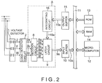
- Fig. 2 is a block diagram showing an apparatus for outputting a signal synchronized with a phase of a power supply according to an embodiment of the invention.
- a voltage detector 1 steps down the voltage on an a.c. bus 17 and outputs the phase voltage signals U, V, W to a logic detector 2.
- the logic detector 2 transforms the voltage signals U, V and W into the corresponding logic level "1" or "0" depending on the polarity of those signals.
- the resulting logic signals 2a to 3c are sent to a decoder circuit 8.
- the decoder circuit 8 serves to decode the logic signals 2a to 2c and output the decoded signals 8a to 8f synchronized with the voltage signals U, V and W.
- Those decoded signals 8a to 8f are sent from the decoder circuit 8 to a latch circuit 9.
- the latch circuit 9 receives the decoded signals 8a to 8f and latches a phase difference angle data 16a output from an integrating circuit 16 at the leading edge and the trailing edge of each of the logic signals 2a to 2c. Then, the latch signal 9 feeds the latched signal as a phase-synchronized signal 9a.
- the latch circuit 9 is connected to an input buffer 10 in which the phase-synchronized signal 9a is temporarily stored as data 10a.
- the data 10a is read by the microcomputer 12 through a bus line 11.
- This microcomputer 12 includes a ROM 13 for storing an operation program and a RAM 14 for storing an operational result processed by the program.
- the microcomputer 12 sends the operational result as the phase difference angle modifying data 15a to the integrating circuit 16 through an output buffer 15.
- This integrating circuit 16 adds (that is, integrates) the phase difference angle modifying data 15 at constant intervals and re-start the integral operation each time the integrated value reaches a predetermined value VC.
- the integrating circuit 16 then sends out the phase difference angle data 16a obtained as an integrated value signal to the latch circuit 9.
- the present embodiment provides a decoder circuit 8, a latch circuit and an integrating circuit 16 enclosed by a dotted line A in place of the ROM 3, the adder 4, the voltage smoothing circuit 5, a voltage oscillating circuit 6, and a frequency dividing circuit 7 provided in the prior art as shown in Fig. 1.
- a voltage detector 1 detects each phase voltage on the a.c. bus 17 and feed the voltage signals U, V, W as shown in a part (a) of Fig. 3.
- the logic detector circuit 2 transforms those voltage signals U, V, W into the logic level “1" or “0” depending on the polarity of each signal and feeds the logic signals as shown in a part (b) of Fig. 3 to a decoder circuit 8.
- the decoder circuit 8 generates pulse signals 8a, 8b, 8c at the leading edges of the logic signals 2a, 2b, 2c and pulse signals 8d, 8e, 8f at the trailing edges of the logic signals 2a, 2b, 2c, respectively.
- the latch circuit 9 latches phase difference angle data 16a (see a part (c) of Fig. 3) sent from the integrating circuit 16 in synchronization with the signals 8a to 8a sent from the decoder circuit 8 (therefore, the leading edges and the trailing edges of the signals 2a to 2c) and then feeds phase-synchronized signals ⁇ u , ⁇ v , ⁇ w , ⁇ x , ⁇ y , ⁇ z as shown in a part (d) of Fig. 3,
- a signal 9a indicates a collection of those signals.
- Those phase-synchronized signals ⁇ u to ⁇ z are respectively allocated to respective addresses of the microcomputer 12.
- the microcomputer 12 can individually read the phase-synchronized signals ⁇ u to ⁇ z through an input buffer 10.
- the microcomputer 12 compares a value of the signal ⁇ u with a phase difference angle command value pre-set in the ROM 13 and performs a proportional plus integral operation of the resulting deviation. Then, the microcomputer 12 obtains such a phase difference angle modifying data as constantly reducing the deviation to zero and feeds the obtained data to the integrating circuit 16 through the output buffer 15 so that the obtained data is added as the phase difference angle modifying data 15a to the integrating circuit 16.
- the deviation is positive.
- the steps are taken of magnifying the phase difference angle modifying data 15a to be input to the integrating circuit 16, reducing a period T of the signal 16a, and thereby sharpening an inclination of the leading edge of the signal 16a.
- the deviation is negative.
- the operation reverse to the above is carried out, resulting in the phase difference angle data ⁇ u being made smaller.
- the microcomputer 12 works to process the other phase-synchronized signals ⁇ u , ⁇ v , ⁇ w , ⁇ x , ⁇ y , ⁇ z in the similar manner.
- the phase-synchronized signals ⁇ u , ⁇ v , ⁇ w , ⁇ x , ⁇ y , ⁇ z are individually corrected. It will be easily understood from the skilled persons in this art that the present invention is not merely limited to this embodiment but may apply to the arrangement which takes the steps of adding those signals and processing the averaged value.
Landscapes
- Engineering & Computer Science (AREA)
- Power Engineering (AREA)
- Stabilization Of Oscillater, Synchronisation, Frequency Synthesizers (AREA)
- Stand-By Power Supply Arrangements (AREA)
- Supply And Distribution Of Alternating Current (AREA)
- Power Conversion In General (AREA)
- Inverter Devices (AREA)
- Control Of Eletrric Generators (AREA)
- Rectifiers (AREA)
Applications Claiming Priority (2)
| Application Number | Priority Date | Filing Date | Title |
|---|---|---|---|
| JP246444/90 | 1990-09-17 | ||
| JP2246444A JP2758258B2 (ja) | 1990-09-17 | 1990-09-17 | 電源同期位相固定装置 |
Publications (2)
| Publication Number | Publication Date |
|---|---|
| EP0476581A1 true EP0476581A1 (de) | 1992-03-25 |
| EP0476581B1 EP0476581B1 (de) | 1993-12-29 |
Family
ID=17148544
Family Applications (1)
| Application Number | Title | Priority Date | Filing Date |
|---|---|---|---|
| EP91115743A Expired - Lifetime EP0476581B1 (de) | 1990-09-17 | 1991-09-17 | Vorrichtung zur Erzeugung eines mit der Phase der Leistungsversorgung synchronisierten digitalen Signals |
Country Status (6)
| Country | Link |
|---|---|
| US (1) | US5285374A (de) |
| EP (1) | EP0476581B1 (de) |
| JP (1) | JP2758258B2 (de) |
| KR (1) | KR950013802B1 (de) |
| DE (1) | DE69100890T2 (de) |
| HK (1) | HK144094A (de) |
Cited By (2)
| Publication number | Priority date | Publication date | Assignee | Title |
|---|---|---|---|---|
| CN109521238A (zh) * | 2018-11-09 | 2019-03-26 | 中电科仪器仪表有限公司 | 一种示波器平台高速总线的解码、触发和分析系统及方法 |
| US20230052260A1 (en) * | 2016-05-05 | 2023-02-16 | Fox Head, Inc. | In-molded helmet chinbar |
Families Citing this family (3)
| Publication number | Priority date | Publication date | Assignee | Title |
|---|---|---|---|---|
| JP3011489B2 (ja) | 1991-06-25 | 2000-02-21 | 株式会社東芝 | 電源同期位相固定装置 |
| US5473533A (en) * | 1993-12-02 | 1995-12-05 | Best Power Technology, Incorporated | Method and apparatus for efficient phase and frequency coherence locking optimized for digital systems |
| CN104579514B (zh) * | 2014-12-10 | 2016-10-05 | 中国航空工业集团公司北京长城计量测试技术研究所 | 一种平衡接口方式下串行数据总线信号的仿真方法 |
Citations (3)
| Publication number | Priority date | Publication date | Assignee | Title |
|---|---|---|---|---|
| DE2941287A1 (de) * | 1979-10-11 | 1981-04-30 | Siemens AG, 1000 Berlin und 8000 München | Digitale zuendsteuervorrichtung fuer stromrichterventile |
| EP0143405A2 (de) * | 1983-11-25 | 1985-06-05 | Kabushiki Kaisha Toshiba | Anordnung zum Ermitteln einer Phase |
| WO1989005065A1 (en) * | 1987-11-18 | 1989-06-01 | Bell Communications Research, Inc. | Digital phase locked loop with bounded jitter |
Family Cites Families (4)
| Publication number | Priority date | Publication date | Assignee | Title |
|---|---|---|---|---|
| US3657732A (en) * | 1968-11-29 | 1972-04-18 | Burroughs Corp | Phase synchronizing system |
| US4484152A (en) * | 1982-05-19 | 1984-11-20 | Westinghouse Electric Corp. | Phase-locked loop having improved locking capabilities |
| DE3719582C2 (de) * | 1987-06-12 | 1999-01-28 | Philips Broadcast Television S | Schaltungsanordnung zur Erzeugung eines Phasenreferenzsignals |
| EP0310088B1 (de) * | 1987-10-01 | 1996-06-05 | Sharp Kabushiki Kaisha | Digitale Phasenregelschleifen-Anordnung |
-
1990
- 1990-09-17 JP JP2246444A patent/JP2758258B2/ja not_active Expired - Lifetime
-
1991
- 1991-09-16 KR KR1019910016123A patent/KR950013802B1/ko not_active Expired - Fee Related
- 1991-09-16 US US07/760,361 patent/US5285374A/en not_active Expired - Lifetime
- 1991-09-17 EP EP91115743A patent/EP0476581B1/de not_active Expired - Lifetime
- 1991-09-17 DE DE69100890T patent/DE69100890T2/de not_active Expired - Fee Related
-
1994
- 1994-12-15 HK HK144094A patent/HK144094A/en not_active IP Right Cessation
Patent Citations (3)
| Publication number | Priority date | Publication date | Assignee | Title |
|---|---|---|---|---|
| DE2941287A1 (de) * | 1979-10-11 | 1981-04-30 | Siemens AG, 1000 Berlin und 8000 München | Digitale zuendsteuervorrichtung fuer stromrichterventile |
| EP0143405A2 (de) * | 1983-11-25 | 1985-06-05 | Kabushiki Kaisha Toshiba | Anordnung zum Ermitteln einer Phase |
| WO1989005065A1 (en) * | 1987-11-18 | 1989-06-01 | Bell Communications Research, Inc. | Digital phase locked loop with bounded jitter |
Cited By (2)
| Publication number | Priority date | Publication date | Assignee | Title |
|---|---|---|---|---|
| US20230052260A1 (en) * | 2016-05-05 | 2023-02-16 | Fox Head, Inc. | In-molded helmet chinbar |
| CN109521238A (zh) * | 2018-11-09 | 2019-03-26 | 中电科仪器仪表有限公司 | 一种示波器平台高速总线的解码、触发和分析系统及方法 |
Also Published As
| Publication number | Publication date |
|---|---|
| JP2758258B2 (ja) | 1998-05-28 |
| US5285374A (en) | 1994-02-08 |
| HK144094A (en) | 1994-12-23 |
| DE69100890T2 (de) | 1994-05-26 |
| KR950013802B1 (ko) | 1995-11-16 |
| DE69100890D1 (de) | 1994-02-10 |
| EP0476581B1 (de) | 1993-12-29 |
| JPH04125032A (ja) | 1992-04-24 |
| KR920007354A (ko) | 1992-04-28 |
Similar Documents
| Publication | Publication Date | Title |
|---|---|---|
| US5410572A (en) | Phase locked loop circuit | |
| EP0428869B1 (de) | Phasendetektor für eine Phasenregelschleife | |
| US5285374A (en) | Apparatus for generating digital signal synchronized with phase of power supply | |
| EP0731564A2 (de) | Verfahren und Vorrichtung zur Bestimmung der Teilerverhältnisses in einem digitalen Phasenregelkreis | |
| US6757349B1 (en) | PLL frequency synthesizer with lock detection circuit | |
| EP0164785A1 (de) | Elektrische Schaltungsanordnung, die eine Phasenkontrollschaltung enthält | |
| US4686482A (en) | Clock signal arrangement for regenerating a clock signal | |
| GB2242796A (en) | Automatic frequency synchronizer | |
| JP2000037079A (ja) | Pwm回路 | |
| JP2736702B2 (ja) | 非同期検出回路 | |
| JPS6236944A (ja) | 搬送波再生方式 | |
| JP3115115B2 (ja) | 自励式インバータ | |
| JPH09146654A (ja) | クロック信号発生装置 | |
| KR0164554B1 (ko) | 수평동기신호를 이용한 비데오 동기신호 검출회로 | |
| US6566965B2 (en) | PLL circuit including a DC power source alarm | |
| JP2853817B2 (ja) | フェイズロックループ | |
| JP2513253B2 (ja) | Pwm方式インバ―タの制御回路 | |
| JPS6359008A (ja) | Fm変調回路 | |
| KR200188170Y1 (ko) | 클럭 발생기 | |
| JP3011489B2 (ja) | 電源同期位相固定装置 | |
| JPH0669912A (ja) | 位相同期発振器 | |
| JPH05211778A (ja) | インバータの位相制御方法並びにインバータの位相制御装置 | |
| JPH04154220A (ja) | 位相同期回路 | |
| JPH06261224A (ja) | Pll回路 | |
| JPS62217862A (ja) | インバ−タ装置 |
Legal Events
| Date | Code | Title | Description |
|---|---|---|---|
| PUAI | Public reference made under article 153(3) epc to a published international application that has entered the european phase |
Free format text: ORIGINAL CODE: 0009012 |
|
| 17P | Request for examination filed |
Effective date: 19910917 |
|
| AK | Designated contracting states |
Kind code of ref document: A1 Designated state(s): DE FR GB |
|
| 17Q | First examination report despatched |
Effective date: 19930302 |
|
| GRAA | (expected) grant |
Free format text: ORIGINAL CODE: 0009210 |
|
| AK | Designated contracting states |
Kind code of ref document: B1 Designated state(s): DE FR GB |
|
| REF | Corresponds to: |
Ref document number: 69100890 Country of ref document: DE Date of ref document: 19940210 |
|
| ET | Fr: translation filed | ||
| PLBE | No opposition filed within time limit |
Free format text: ORIGINAL CODE: 0009261 |
|
| STAA | Information on the status of an ep patent application or granted ep patent |
Free format text: STATUS: NO OPPOSITION FILED WITHIN TIME LIMIT |
|
| 26N | No opposition filed | ||
| PGFP | Annual fee paid to national office [announced via postgrant information from national office to epo] |
Ref country code: FR Payment date: 19960910 Year of fee payment: 6 |
|
| PG25 | Lapsed in a contracting state [announced via postgrant information from national office to epo] |
Ref country code: FR Free format text: THE PATENT HAS BEEN ANNULLED BY A DECISION OF A NATIONAL AUTHORITY Effective date: 19970930 |
|
| REG | Reference to a national code |
Ref country code: FR Ref legal event code: ST |
|
| REG | Reference to a national code |
Ref country code: GB Ref legal event code: 746 Effective date: 19981103 |
|
| REG | Reference to a national code |
Ref country code: GB Ref legal event code: IF02 |
|
| PGFP | Annual fee paid to national office [announced via postgrant information from national office to epo] |
Ref country code: GB Payment date: 20060913 Year of fee payment: 16 |
|
| PGFP | Annual fee paid to national office [announced via postgrant information from national office to epo] |
Ref country code: DE Payment date: 20060914 Year of fee payment: 16 |
|
| GBPC | Gb: european patent ceased through non-payment of renewal fee |
Effective date: 20070917 |
|
| PG25 | Lapsed in a contracting state [announced via postgrant information from national office to epo] |
Ref country code: DE Free format text: LAPSE BECAUSE OF NON-PAYMENT OF DUE FEES Effective date: 20080401 |
|
| PG25 | Lapsed in a contracting state [announced via postgrant information from national office to epo] |
Ref country code: GB Free format text: LAPSE BECAUSE OF NON-PAYMENT OF DUE FEES Effective date: 20070917 |