EP0477367A1 - Vorrichtung zur verhinderung des einschaltstromes in elektrische apparate - Google Patents
Vorrichtung zur verhinderung des einschaltstromes in elektrische apparate Download PDFInfo
- Publication number
- EP0477367A1 EP0477367A1 EP19900903945 EP90903945A EP0477367A1 EP 0477367 A1 EP0477367 A1 EP 0477367A1 EP 19900903945 EP19900903945 EP 19900903945 EP 90903945 A EP90903945 A EP 90903945A EP 0477367 A1 EP0477367 A1 EP 0477367A1
- Authority
- EP
- European Patent Office
- Prior art keywords
- power source
- rectifier circuit
- voltage
- capacitor
- power
- Prior art date
- Legal status (The legal status is an assumption and is not a legal conclusion. Google has not performed a legal analysis and makes no representation as to the accuracy of the status listed.)
- Granted
Links
Images


Classifications
-
- H—ELECTRICITY
- H02—GENERATION; CONVERSION OR DISTRIBUTION OF ELECTRIC POWER
- H02H—EMERGENCY PROTECTIVE CIRCUIT ARRANGEMENTS
- H02H9/00—Emergency protective circuit arrangements for limiting excess current or voltage without disconnection
- H02H9/001—Emergency protective circuit arrangements for limiting excess current or voltage without disconnection limiting speed of change of electric quantities, e.g. soft switching on or off
Definitions
- the present invention relates to an apparatus for preventing a rush current in various types of electrical devices provided with an alternating current power source, and more particularly, to a rush current preventing apparatus provided in a motor driving device and capable of eliminating an occurrence of a rush current at recovery from an instantaneous stoppage of power supply, to thereby protect the component parts in the circuitry of the motor driving device.
- a.c. power source for example, a motor driving device
- a rectifier circuit connected to the a.c. power source
- an inverter supplied with d.c. power from the rectifier circuit, and are so arranged as to control the load of the various electrical devices, e.g., the current supplied to the motor, by means of the inverter.
- electric power is supplied to the inverter from an electrolytic capacitor which is provided in the rectifier circuit and functions as a smoothing capacitor, and thereafter the voltage across the electrolytic capacitor is gradually reduced. Then, when the power source recovers from the interrupted state, an excessive charging current (rush current) flows through the electrolytic capacitor, which may result in the breakdown of the components in the circuitry of the electrical devices, such as the inverter.
- An object of the present invention is to provide a rush current preventing apparatus which can eliminate the occurrence of a rush current at recovery from an instantaneous stoppage of power supply and thereby protect the component parts in the circuitry of electrical devices equipped with an a.c. power source.
- a rush current preventing apparatus for an electrical device having an a.c. power source and a rectifier circuit connected to the a.c. power source, which comprises a main switch provided between the a.c. power source and the rectifier circuit, series circuit means composed of a current-limiting resistor and an auxiliary switch and provided between the a.c. power source and the rectifier circuit, detecting means for detecting an output voltage of the rectifier circuit and producing a detection output representing a result of comparison between the detected output voltage and a preset voltage, and switch control means responsive to the detection output from the detecting means to turn on one of the main switch and the auxiliary switch and turn off the other of these switches.
- one of the main switch and the auxiliary switch of the series circuit is turned on and the other of the two is turned off in accordance with the result of the comparison between the output voltage of the rectifier circuit and the preset voltage. Accordingly, when the a.c. power source recovers from an instantaneously interrupted state, the a.c. power source can be connected to the rectifier circuit through the current-limiting resistor of the series circuit means, by turning on the auxiliary switch, and thereafter the main switch is turned on, to thereby connect the a.c. power source to the rectifier circuit through the main switch. Therefore, a rush current can be prevented from occurring at the recovery from an instantaneous interruption of the power supply, thereby preventing the breakdown of the component parts in the circuitry of the electrical device equipped with an a.c. power source.
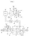
- a motor driving device provided with a rush current preventing apparatus comprises a three-phase alternating current power source 10 having U-, V- and W-phase output terminals, and a three-phase full-wave rectifier circuit 12 having U-, V- and W-phase input terminals.
- a.c. power source 10 and the rectifier circuit 12 are provided between the a.c. power source 10 and the rectifier circuit 12 .
- an electromagnetic contactor MCC and a relay RL2 which respectively serve as a main switch and an auxiliary switch and are connected in parallel to each other.
- the electromagnetic contactor MCC has three relay contacts interposed between the U-, V- and W-phase output terminals of the a.c. power source 10 and the U-, V- and W-phase input terminals of the full-wave rectifier circuit 12, and a relay RL1 for driving these relay contacts.
- the relay RL2 has two relay contacts r12, which are respectively connected at their one ends to the U- and V-phase output terminals of the a.c. power source 10, and connected at the other ends thereof to respective one ends of two current-limiting resistors R and R having other ends thereof respectively connected to the U- and V-phase input terminals of the rectifier circuit 12.
- the motor driving device further comprises a power transistor regenerative circuit 14, an electrolytic capacitor 16 for smoothing the output voltage of the rectifier circuit 12, and an inverter circuit 18 supplied with direct current power from the electrolytic capacitor for controlling a motor 20.
- the rush current preventing apparatus further comprises a latch circuit 28 connected to the processor 26, a first transistor T1 connected to a first output terminal of the latch circuit 28 for switching on and off the relay RL2, and a second transistor T2 connected to a second output terminal of the latch circuit 28 for switching on and off a relay RL3.
- the relay RL3 has a relay contact r13 interposed between the V- and W-phase output terminals of the a.c. power source 10.
- the aforementioned elements 22, 24, 26, 28, RL2, RL3, T1 and T2 are connected to an operating power source provided separately from the a.c. power source 10.
- the processor 26 of the rush current preventing apparatus periodically executes the switch control process shown in Fig. 2.
- the processor 26 first reads the digital output of the A/D converter 24 representing the DC link voltage VDC (step S1), and determines whether or not the DC link voltage VDC is smaller than a preset voltage VS (step S2).
- the voltage VS is previously set to a value smaller than the DC link voltage that can be produced in a normal state. Therefore, as far as the DC link voltage is normal, the determination result in step S2 is negative (NO), and thus the flow proceeds to step S3, wherein the processor 26 sends a first control output to the latch circuit 28.
- the latch circuit 28 delivers a low-level output and a high-level output respectively from the first and second output terminals thereof.
- the first transistor T1 is rendered nonconductive, whereby the relay RL2 is rendered inoperative with the two relay contacts r12 thereof open.
- the second transistor T2 is rendered conductive, and thus the relay RL3 is made operative with the relay contact r13 thereof closed.
- the relay RL1 of the electromagnetic contactor MCC is rendered operative with the three associated relay contacts closed, whereby the output terminals associated with the individual phases of the a.c. power source 10 are connected respectively to the input terminals of the individual phases of the rectifier circuit 12 via the relay contacts (main switch) of the electromagnetic contactor MCC.
- a.c. power supplied from the a.c. power source 10 is rectified into d.c. power in the rectifier circuit 12, and the electrolytic capacitor 16 is charged with the d.c. power.
- the d.c. power smoothed by the electrolytic capacitor 16 is supplied to the inverter 18, which then drives the motor 20.
- step S2 If an instantaneous interruption of power supply occurs in the a.c. power source 10 during motor operation and thus the output voltage of the a.c. power source 10 drops to zero, as shown in Fig. 3, the electrolytic capacitor 16 is discharged and the DC link voltage VDC is gradually reduced.
- the processor 26 sends a second control output to the latch circuit 28 (step S4).
- the latch circuit 28 delivers a high-level output and a low-level output respectively from its first and second output terminals.
- the first transistor T1 is rendered conductive, and the relay RL2 is rendered operative with the two relay contacts r12 thereof closed, whereby the U- and V-phase output terminals of the a.c. power source 10 are connected respectively to the U- and V-phase input terminals of the rectifier circuit 12 via the relay contacts r12 and the current-limiting resistors R and R.
- the second transistor T2 is rendered nonconductive, and thus the relay RL3 is made inoperative with the relay contact r13 thereof opened.
- the relay RL1 of the electromagnetic contactor MCC is rendered inoperative with the three relay contacts thereof open.
- the electrolytic capacitor 16 is charged with the output power of the a.c. power source 10 supplied through the relay contacts (auxiliary switch) r12 associated with the relay RL2, the current-limiting resistors R and R, and the rectifier circuit 12.
- the electric current I supplied from the a.c. power source 10 to the electrolytic capacitor 16 to charge the same is limited by the current-limiting resistors R and R. Accordingly, even at the time of recovery from a power-supply interrupted state in which the DC link voltage VDC is reduced to a low level, an overcurrent I0 (indicated by dashed line in Fig.
- step S3 When the DC link voltage VDC becomes higher than the preset voltage VS, this is detected in the immediately following detection period (step S2), and step S3 is entered.
- step S3 as mentioned above, the first transistor T1 is rendered nonconductive and the relay contacts r12 associated with the relay RL2 are opened, while the second transistor T2 is rendered conductive and thus the relay contact r13 of the relay RL3 is closed, whereby a.c. power is supplied from the a.c. power source 10 directly to the rectifier circuit 12, not by way of the current-limiting resistors R and R, and the electrolytic capacitor 16 is charged with the d.c. power supplied from the rectifier circuit 12.
- the voltage VDC across the electrolytic capacitor 16 is already increased to a considerably high level, and accordingly, no overcurrent is produced even though the electrolytic capacitor 16 is charged with the power which is not passed through the current-limiting resistors R and R.
- the rush current preventing apparatus of the present invention is applied to a motor driving device
- the invention may be applied to various types of electrical devices equipped with an a.c. power source.
- the occurrence of a rush current at recovery from an interrupted state of the a.c. power source of the various electrical devices can be prevented, as in the embodiment, and therefore, the component parts of the circuitry in the various electrical devices can be protected.
Landscapes
- Inverter Devices (AREA)
- Rectifiers (AREA)
- Emergency Protection Circuit Devices (AREA)
Applications Claiming Priority (3)
| Application Number | Priority Date | Filing Date | Title |
|---|---|---|---|
| JP48481/89 | 1989-03-02 | ||
| JP4848189A JPH02231922A (ja) | 1989-03-02 | 1989-03-02 | モータ駆動装置における瞬時停電回復時の突入電流防止制御方式 |
| PCT/JP1990/000277 WO1990010333A1 (fr) | 1989-03-02 | 1990-03-02 | Dispositif pour empecher la penetration de courants de demarrage dans des appareils electriques |
Publications (3)
| Publication Number | Publication Date |
|---|---|
| EP0477367A1 true EP0477367A1 (de) | 1992-04-01 |
| EP0477367A4 EP0477367A4 (en) | 1992-08-05 |
| EP0477367B1 EP0477367B1 (de) | 1994-10-12 |
Family
ID=12804578
Family Applications (1)
| Application Number | Title | Priority Date | Filing Date |
|---|---|---|---|
| EP90903945A Expired - Lifetime EP0477367B1 (de) | 1989-03-02 | 1990-03-02 | Vorrichtung zur verhinderung des einschaltstromes in elektrische apparate |
Country Status (4)
| Country | Link |
|---|---|
| EP (1) | EP0477367B1 (de) |
| JP (1) | JPH02231922A (de) |
| DE (1) | DE69013346T2 (de) |
| WO (1) | WO1990010333A1 (de) |
Cited By (10)
| Publication number | Priority date | Publication date | Assignee | Title |
|---|---|---|---|---|
| WO1996010862A1 (en) * | 1994-09-30 | 1996-04-11 | Telefonaktiebolaget Lm Ericsson | Rectifier bridge apparatus |
| EP0892480A1 (de) * | 1997-07-15 | 1999-01-20 | Ascom Energy Systems AG | AC/DC Spannungsumrichter |
| FR2771863A1 (fr) * | 1997-12-01 | 1999-06-04 | Renault | Dispositif de precharge d'un reseau electrique de puissance |
| EP1101265B1 (de) * | 1998-07-24 | 2002-10-30 | Siemens Aktiengesellschaft | Schaltungsanordnung zur einschaltstrombegrenzung einer kapazitiven last |
| EP1755209A1 (de) * | 2005-08-18 | 2007-02-21 | Samsung Electronics Co., Ltd. | Dreiphasengleichrichter mit Einschaltstrombegrenzungsschaltung |
| FR2907983A1 (fr) * | 2006-10-31 | 2008-05-02 | Airbus France Sas | Dispositif de commande de precharge d'un convertisseur a decoupage, ensemble et aeronef le comportant |
| EP1592105A3 (de) * | 2004-04-26 | 2009-02-25 | Dr. Johannes Heidenhain GmbH | Schutzschaltung für einen Umrichter |
| EP2001096A4 (de) * | 2006-03-29 | 2015-08-12 | Daikin Ind Ltd | Steuerung |
| CN110022053A (zh) * | 2019-03-29 | 2019-07-16 | 合肥华耀电子工业有限公司 | 一种带输入浪涌电流抑制功能的三相整流保护电路 |
| EP4050781A4 (de) * | 2019-11-22 | 2022-12-21 | Huawei Digital Power Technologies Co., Ltd. | Vorladeschaltung, wechselrichter und stromerzeugungssystem |
Families Citing this family (5)
| Publication number | Priority date | Publication date | Assignee | Title |
|---|---|---|---|---|
| DE10018372C2 (de) * | 2000-04-13 | 2003-12-04 | Siemens Ag | Schaltungsanordnung zur Einschaltstrombegrenzung für eine Stromversorgung |
| KR100403964B1 (ko) * | 2001-09-19 | 2003-10-30 | 서장흠 | 모터의 절연저항 측정장치 |
| DE10255012B4 (de) * | 2002-11-25 | 2021-08-05 | Siemens Schweiz Ag | Schaltung zur Begrenzung der beim Schalten von kapazitiven/induktiven Lastkomponenten auftretenden Stromspitzen |
| JP4797700B2 (ja) * | 2006-03-01 | 2011-10-19 | パナソニック株式会社 | モータ制御装置 |
| RU2554795C2 (ru) * | 2009-09-21 | 2015-06-27 | Мериал Лимитед | Водная суспензия длительного хранения на основе дицикланила и составы из неводной суспензии для применения путем промывания и опрыскивания, пригодные для профилактики и лечения заражения насекомыми у животных |
Family Cites Families (5)
| Publication number | Priority date | Publication date | Assignee | Title |
|---|---|---|---|---|
| US4397455A (en) * | 1977-02-04 | 1983-08-09 | Docutel Corporation | Document dispenser with escrow system |
| DE3122835C2 (de) * | 1981-06-09 | 1987-03-26 | Siemens AG, 1000 Berlin und 8000 München | Schaltungsanordnung zur Einschaltstrombegrenzung |
| JPS6024195U (ja) * | 1983-07-20 | 1985-02-19 | 松下電工株式会社 | インバ−タ装置 |
| JPS60156225A (ja) * | 1984-01-25 | 1985-08-16 | 松下電工株式会社 | 電源回路 |
| US4573113A (en) * | 1984-01-26 | 1986-02-25 | Borg-Warner Corporation | Surge protection system for a d-c power supply during power-up |
-
1989
- 1989-03-02 JP JP4848189A patent/JPH02231922A/ja active Pending
-
1990
- 1990-03-02 DE DE69013346T patent/DE69013346T2/de not_active Expired - Fee Related
- 1990-03-02 WO PCT/JP1990/000277 patent/WO1990010333A1/ja not_active Ceased
- 1990-03-02 EP EP90903945A patent/EP0477367B1/de not_active Expired - Lifetime
Cited By (16)
| Publication number | Priority date | Publication date | Assignee | Title |
|---|---|---|---|---|
| US5687069A (en) * | 1994-09-30 | 1997-11-11 | Telefonaktiebolaget Lm Ericsson | Rectifier bridge apparatus |
| CN1047041C (zh) * | 1994-09-30 | 1999-12-01 | 艾利森电话股份有限公司 | 整流电桥装置 |
| WO1996010862A1 (en) * | 1994-09-30 | 1996-04-11 | Telefonaktiebolaget Lm Ericsson | Rectifier bridge apparatus |
| EP0892480A1 (de) * | 1997-07-15 | 1999-01-20 | Ascom Energy Systems AG | AC/DC Spannungsumrichter |
| FR2771863A1 (fr) * | 1997-12-01 | 1999-06-04 | Renault | Dispositif de precharge d'un reseau electrique de puissance |
| WO1999029007A1 (fr) * | 1997-12-01 | 1999-06-10 | Renault | Dispositif de precharge d'un reseau electrique de puissance |
| EP1101265B1 (de) * | 1998-07-24 | 2002-10-30 | Siemens Aktiengesellschaft | Schaltungsanordnung zur einschaltstrombegrenzung einer kapazitiven last |
| EP1592105A3 (de) * | 2004-04-26 | 2009-02-25 | Dr. Johannes Heidenhain GmbH | Schutzschaltung für einen Umrichter |
| US7529068B2 (en) | 2004-04-26 | 2009-05-05 | Dr. Johannes Heidenhain Gmbh | Protective circuit for a frequency converter |
| EP1755209A1 (de) * | 2005-08-18 | 2007-02-21 | Samsung Electronics Co., Ltd. | Dreiphasengleichrichter mit Einschaltstrombegrenzungsschaltung |
| EP2001096A4 (de) * | 2006-03-29 | 2015-08-12 | Daikin Ind Ltd | Steuerung |
| FR2907983A1 (fr) * | 2006-10-31 | 2008-05-02 | Airbus France Sas | Dispositif de commande de precharge d'un convertisseur a decoupage, ensemble et aeronef le comportant |
| CN110022053A (zh) * | 2019-03-29 | 2019-07-16 | 合肥华耀电子工业有限公司 | 一种带输入浪涌电流抑制功能的三相整流保护电路 |
| CN110022053B (zh) * | 2019-03-29 | 2024-03-29 | 合肥华耀电子工业有限公司 | 一种带输入浪涌电流抑制功能的三相整流保护电路 |
| EP4050781A4 (de) * | 2019-11-22 | 2022-12-21 | Huawei Digital Power Technologies Co., Ltd. | Vorladeschaltung, wechselrichter und stromerzeugungssystem |
| US11722001B2 (en) | 2019-11-22 | 2023-08-08 | Huawei Digital Power Technologies Co., Ltd. | Pre-charging circuit, inverter, and power generation system |
Also Published As
| Publication number | Publication date |
|---|---|
| JPH02231922A (ja) | 1990-09-13 |
| DE69013346T2 (de) | 1995-02-16 |
| WO1990010333A1 (fr) | 1990-09-07 |
| DE69013346D1 (de) | 1994-11-17 |
| EP0477367A4 (en) | 1992-08-05 |
| EP0477367B1 (de) | 1994-10-12 |
Similar Documents
| Publication | Publication Date | Title |
|---|---|---|
| JP2903863B2 (ja) | インバータ装置 | |
| EP0488240B1 (de) | Wechselrichter versehen mit einem Kreis zur Regelung der elektrischen Entladung eines Gleichstrom-Glättungskondensators und Verfahren zur Regelung desselben | |
| EP0477367B1 (de) | Vorrichtung zur verhinderung des einschaltstromes in elektrische apparate | |
| EP0739075B1 (de) | Stromversorgungssystem | |
| JP3428242B2 (ja) | 無停電電源装置 | |
| JP2004112929A (ja) | 交流−直流変換装置 | |
| JPH06245485A (ja) | インバータ装置 | |
| JP2839638B2 (ja) | エレベータの制御装置 | |
| JP3713429B2 (ja) | オフラインupsシステム | |
| JPH07288979A (ja) | コンバータ回路および電動射出成形機 | |
| JPH0531788Y2 (de) | ||
| JPS60176467A (ja) | 電力変換装置 | |
| JP3336086B2 (ja) | インバータの入力欠相保護装置 | |
| JPS62250876A (ja) | 電圧形インバ−タ装置 | |
| JPH03212167A (ja) | インバータの過電圧検出装置 | |
| JPS63124766A (ja) | 突入電流制限回路 | |
| JP2638982B2 (ja) | 初期充電方法 | |
| JPS5915263Y2 (ja) | 周波数変換器 | |
| JPH0510020B2 (de) | ||
| JPH1023740A (ja) | 電力変換装置 | |
| JPH0947030A (ja) | インバータ装置 | |
| JP3267427B2 (ja) | 起動回路を有する電源装置 | |
| SU1494094A2 (ru) | Устройство дл автоматического повторного включени асинхронного электродвигател | |
| JP3601255B2 (ja) | インバータ装置の負荷短絡検出方法 | |
| JPH1052051A (ja) | パルス幅変調コンバータ装置 |
Legal Events
| Date | Code | Title | Description |
|---|---|---|---|
| PUAI | Public reference made under article 153(3) epc to a published international application that has entered the european phase |
Free format text: ORIGINAL CODE: 0009012 |
|
| 17P | Request for examination filed |
Effective date: 19901116 |
|
| AK | Designated contracting states |
Kind code of ref document: A1 Designated state(s): CH DE GB LI |
|
| A4 | Supplementary search report drawn up and despatched |
Effective date: 19920615 |
|
| AK | Designated contracting states |
Kind code of ref document: A4 Designated state(s): CH DE GB LI |
|
| RIN1 | Information on inventor provided before grant (corrected) |
Inventor name: SASUGA, EIICHI Inventor name: KONO, SHINICHI, ROOM 7-203 FANUC MANSHONHARIMOMI |
|
| 17Q | First examination report despatched |
Effective date: 19930826 |
|
| GRAA | (expected) grant |
Free format text: ORIGINAL CODE: 0009210 |
|
| AK | Designated contracting states |
Kind code of ref document: B1 Designated state(s): CH DE GB LI |
|
| PG25 | Lapsed in a contracting state [announced via postgrant information from national office to epo] |
Ref country code: LI Effective date: 19941012 Ref country code: CH Effective date: 19941012 |
|
| REF | Corresponds to: |
Ref document number: 69013346 Country of ref document: DE Date of ref document: 19941117 |
|
| REG | Reference to a national code |
Ref country code: CH Ref legal event code: PL |
|
| PG25 | Lapsed in a contracting state [announced via postgrant information from national office to epo] |
Ref country code: GB Effective date: 19950302 |
|
| PLBE | No opposition filed within time limit |
Free format text: ORIGINAL CODE: 0009261 |
|
| 26N | No opposition filed | ||
| GBPC | Gb: european patent ceased through non-payment of renewal fee |
Effective date: 19950302 |
|
| PGFP | Annual fee paid to national office [announced via postgrant information from national office to epo] |
Ref country code: DE Payment date: 19960313 Year of fee payment: 7 |
|
| PG25 | Lapsed in a contracting state [announced via postgrant information from national office to epo] |
Ref country code: DE Effective date: 19971202 |