EP0477594A1 - Thyristor à passage à l'ouverture - Google Patents
Thyristor à passage à l'ouverture Download PDFInfo
- Publication number
- EP0477594A1 EP0477594A1 EP91114768A EP91114768A EP0477594A1 EP 0477594 A1 EP0477594 A1 EP 0477594A1 EP 91114768 A EP91114768 A EP 91114768A EP 91114768 A EP91114768 A EP 91114768A EP 0477594 A1 EP0477594 A1 EP 0477594A1
- Authority
- EP
- European Patent Office
- Prior art keywords
- conductivity type
- emitter
- base
- connection
- thyristor
- Prior art date
- Legal status (The legal status is an assumption and is not a legal conclusion. Google has not performed a legal analysis and makes no representation as to the accuracy of the status listed.)
- Granted
Links
- 239000004065 semiconductor Substances 0.000 claims abstract description 21
- 230000005669 field effect Effects 0.000 claims abstract description 13
- 239000010409 thin film Substances 0.000 claims abstract description 4
- 238000002513 implantation Methods 0.000 description 3
- 239000000463 material Substances 0.000 description 3
- XKRFYHLGVUSROY-UHFFFAOYSA-N Argon Chemical compound [Ar] XKRFYHLGVUSROY-UHFFFAOYSA-N 0.000 description 2
- IJGRMHOSHXDMSA-UHFFFAOYSA-N Atomic nitrogen Chemical compound N#N IJGRMHOSHXDMSA-UHFFFAOYSA-N 0.000 description 2
- 238000011161 development Methods 0.000 description 2
- 230000018109 developmental process Effects 0.000 description 2
- 238000009413 insulation Methods 0.000 description 2
- 150000002500 ions Chemical class 0.000 description 2
- ZOXJGFHDIHLPTG-UHFFFAOYSA-N Boron Chemical compound [B] ZOXJGFHDIHLPTG-UHFFFAOYSA-N 0.000 description 1
- 229910052786 argon Inorganic materials 0.000 description 1
- 229910052796 boron Inorganic materials 0.000 description 1
- 239000013078 crystal Substances 0.000 description 1
- 230000006378 damage Effects 0.000 description 1
- 230000001066 destructive effect Effects 0.000 description 1
- 239000002019 doping agent Substances 0.000 description 1
- 239000001307 helium Substances 0.000 description 1
- 229910052734 helium Inorganic materials 0.000 description 1
- SWQJXJOGLNCZEY-UHFFFAOYSA-N helium atom Chemical compound [He] SWQJXJOGLNCZEY-UHFFFAOYSA-N 0.000 description 1
- 229910052757 nitrogen Inorganic materials 0.000 description 1
- 229910052710 silicon Inorganic materials 0.000 description 1
- 239000010703 silicon Substances 0.000 description 1
- 239000000126 substance Substances 0.000 description 1
Images
Classifications
-
- H—ELECTRICITY
- H10—SEMICONDUCTOR DEVICES; ELECTRIC SOLID-STATE DEVICES NOT OTHERWISE PROVIDED FOR
- H10D—INORGANIC ELECTRIC SEMICONDUCTOR DEVICES
- H10D18/00—Thyristors
- H10D18/60—Gate-turn-off devices
- H10D18/65—Gate-turn-off devices with turn-off by field effect
- H10D18/655—Gate-turn-off devices with turn-off by field effect produced by insulated gate structures
-
- H—ELECTRICITY
- H10—SEMICONDUCTOR DEVICES; ELECTRIC SOLID-STATE DEVICES NOT OTHERWISE PROVIDED FOR
- H10D—INORGANIC ELECTRIC SEMICONDUCTOR DEVICES
- H10D62/00—Semiconductor bodies, or regions thereof, of devices having potential barriers
- H10D62/10—Shapes, relative sizes or dispositions of the regions of the semiconductor bodies; Shapes of the semiconductor bodies
- H10D62/113—Isolations within a component, i.e. internal isolations
- H10D62/115—Dielectric isolations, e.g. air gaps
-
- H—ELECTRICITY
- H10—SEMICONDUCTOR DEVICES; ELECTRIC SOLID-STATE DEVICES NOT OTHERWISE PROVIDED FOR
- H10D—INORGANIC ELECTRIC SEMICONDUCTOR DEVICES
- H10D62/00—Semiconductor bodies, or regions thereof, of devices having potential barriers
- H10D62/10—Shapes, relative sizes or dispositions of the regions of the semiconductor bodies; Shapes of the semiconductor bodies
- H10D62/17—Semiconductor regions connected to electrodes not carrying current to be rectified, amplified or switched, e.g. channel regions
- H10D62/192—Base regions of thyristors
- H10D62/206—Cathode base regions of thyristors
-
- H—ELECTRICITY
- H10—SEMICONDUCTOR DEVICES; ELECTRIC SOLID-STATE DEVICES NOT OTHERWISE PROVIDED FOR
- H10D—INORGANIC ELECTRIC SEMICONDUCTOR DEVICES
- H10D62/00—Semiconductor bodies, or regions thereof, of devices having potential barriers
- H10D62/50—Physical imperfections
- H10D62/53—Physical imperfections the imperfections being within the semiconductor body
Definitions
- the invention relates to a thyristor that can be switched off in accordance with the same generic terms of claims 1 and 2.
- each emitter region is connected to the first main connection via an individually assigned resistance element and in which the resistance element is in particular formed as a covering made of resistive material, which is formed on a the first main surface covering, electrically insulating layer is applied.
- the resistance element is in particular formed as a covering made of resistive material, which is formed on a the first main surface covering, electrically insulating layer is applied.
- the invention has for its object to provide a thyristor of the type mentioned, in which thermal destruction when switching off is safely avoided without the resistance elements used to increase the voltage drop across the thyristor in the on state. This is achieved according to the invention by training according to the characterizing parts of claims 1 or 2.
- the advantage that can be achieved with the invention is, in particular, that the resistance elements integrated in the emitter structures of the thyristor, designed as switchable field-effect transistors, cause only a very small voltage drop in the on state of the thyristor, while when the thyristor is switched off they each connect the emitter regions to the first main connection interrupt completely.
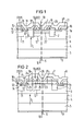
- FIG. 1 schematically shows part of a thyristor that can be switched off and has a semiconductor body 1 consisting of doped semiconductor material, for example silicon, in section.
- the part shown contains an n-type emitter region 2, which is inserted into a p-type layer 3, which forms the p-base.
- An underlying n-type layer represents the n-base 4, while the lowest, p-type layer forms the p-emitter 5 of the thyristor.
- the emitter region 2, which starts from the upper main surface 1 of the thyristor, has, for example, a self-contained, approximately hollow cylindrical shape that is symmetrical about a vertical axis 6.
- This area could, for example, be that of a rectangular or square frame oriented in the lateral direction.
- a further cross section which is placed through the axis 6 perpendicular to the image plane of FIG. 1, would be congruent with the previously described cross section of FIG. 1.
- the switchable thyristor is composed of many parts designed in accordance with FIG are arranged one behind the other. Layers 3 to 5 are designed as layers running over the entire thyristor cross section, while emitter region 2, together with the corresponding emitter regions of the other parts, forms the top, n-conducting layer of the thyristor and thus the n-emitter of the same.
- the n-emitter region 2 is connected via a resistance element to be described later with a conductive assignment 7, which is connected to a main connection 8 on the cathode side.
- the p-emitter 5 is provided with an anode-side electrode 9, which is connected to a second, anode-side main connection 10.
- the conductive assignment 7 connects the n-emitter regions of all thyristor parts to the first main connection 8, while the anode-side electrode 9 is common to all thyristor parts.
- an electrode 11 assigned to it is provided, which consists of part of the conductive assignment 7 and is thus also conductively connected to the main connection 8.
- the electrode 11 contacts a p-type semiconductor zone 12, which is inserted into a lateral extension 13 of the n-emitter region 2.
- Zone 12 forms a first field effect transistor T1, which connects the p-base 3 with the conductive assignment 7 and further to the main terminal 8.
- This connection represents a switch-off current path for the thyristor part shown.
- the gate electrode 16 is connected to the corresponding gate electrodes of the other thyristor parts at a common gate connection 17.
- the resistance element which connects the n-emitter region 2 to the conductive assignment 7, consists of a second field effect transistor T2.
- This comprises an edge-side part of the n-emitter region 2, an n- inserted into the p-base 3 conductive semiconductor region 18 and a part of the p-base 3 lying between 2 and 18 and adjoining the main surface 1 and which is covered by a gate electrode 19.
- This is separated from the main surface 1 by a thin, electrically insulating layer 20.
- the gate electrode 19 has a connection 19a. With 21, the parts 16 and 19 from the conductive covering 7 separating intermediate insulation layer, for example made of Si0 2 , is designated.
- a part I L of the load current which is attributable to the thyristor part shown flows from the main connection 10 via the electrode 9 to the n-emitter region 2 and from there via the transistor T2, by means of a positive voltage supplied to the connection 19a U2 is switched to assignment 7 and via this to main terminal 8.
- T1 is blocked by supplying a positive voltage U1 to terminal 17.
- T1 When the thyristor is switched off, T1 is now turned on by supplying a negative voltage U1 to connection 17, while T2 is blocked by supplying a negative voltage U2 to connection 19a.
- the load current component L is thus no longer supplied to the n-emitter region 2, but rather via the switched-off cut-off current path 3, 14, 12 and 11 of the assignment 7 and thus the main connection 8, so that the thyristor is extinguished.
- a considerable voltage drops across the blocked transistor T2, which is also supplied to the semiconductor zone 12 via the conductive assignment 7, so that the deflection of the load current component I L shown on the switch-off current path is reliably accomplished.
- an insulating layer 22 is inserted into the p-base 3 below the n-conducting semiconductor 18 in order to make the cut-off current path 3, 14, 12, 11, 8 clearly different from the load current path in the current-carrying operating state of the thyristor to distinguish.
- the insulating layer 22 can be produced by deep implantation of 0 2 ions into the semiconductor body 1.
- a possible alternative to this is to form the layer 22 not as an insulating layer, but as a layer with a greatly reduced carrier life. This is preferably achieved by deep implantation of ions of a substance such as argon, helium or nitrogen, which destroys the crystal lattice of the semiconductor body within the layer 22.
- the layer 22 can also be formed as a highly doped p-zone, which can be carried out by deep implantation of the dopant used for doping the p-base 3, for example boron.
- the exemplary embodiment of the invention shown in FIG. 2 has the same structure within the semiconductor body 1 as the exemplary embodiment according to FIG. 1. Only the semiconductor region 18 is omitted.
- the field effect transistor T2 which represents the resistance element, is implemented here using thin-film technology.
- a thin, electrically insulating layer 23 is applied in the area of the n-emitter region 2 on the main surface 1 a.
- a layer of doped semiconductor material is then epitaxially grown on the layer 23 and has a first, n - doped connection region 24, a second, n ⁇ - doped connection region 26 and an intermediate p-doped channel region 27.
- connection region 24 contacts the n-emitter region 2 in a contact hole 25 of the insulating layer 23.
- the channel region 27 is covered by an insulating layer 28, on which the gate electrode 19 of T2 is then applied. With 29 an intermediate insulation layer is designated, which electrically isolates the gate electrodes 16 and 19 from the conductive assignment 7.
- the mode of operation of the exemplary embodiment according to FIG. 2 corresponds to that of the exemplary embodiment according to FIG. 1.
Landscapes
- Thyristors (AREA)
Applications Claiming Priority (2)
| Application Number | Priority Date | Filing Date | Title |
|---|---|---|---|
| DE4030299 | 1990-09-25 | ||
| DE4030299 | 1990-09-25 |
Publications (2)
| Publication Number | Publication Date |
|---|---|
| EP0477594A1 true EP0477594A1 (fr) | 1992-04-01 |
| EP0477594B1 EP0477594B1 (fr) | 1996-01-17 |
Family
ID=6414932
Family Applications (1)
| Application Number | Title | Priority Date | Filing Date |
|---|---|---|---|
| EP91114768A Expired - Lifetime EP0477594B1 (fr) | 1990-09-25 | 1991-09-02 | Thyristor à passage à l'ouverture |
Country Status (4)
| Country | Link |
|---|---|
| US (1) | US5291040A (fr) |
| EP (1) | EP0477594B1 (fr) |
| JP (1) | JP3165480B2 (fr) |
| DE (1) | DE59107276D1 (fr) |
Cited By (4)
| Publication number | Priority date | Publication date | Assignee | Title |
|---|---|---|---|---|
| WO1992012541A1 (fr) * | 1991-01-09 | 1992-07-23 | Fraunhofer-Gesellschaft zur Förderung der angewandten Forschung e.V. | Structure integree d'un interrupteur de puissance |
| FR2688631A1 (fr) * | 1992-03-16 | 1993-09-17 | Mitsubishi Electric Corp | Dispositif semi-conducteur ayant un courant maximum controlable important et procede pour sa fabrication. |
| EP0555047A3 (en) * | 1992-02-03 | 1993-10-13 | Fuji Electric Co., Ltd. | Semiconductor gated switching device |
| WO1995021461A1 (fr) * | 1994-02-01 | 1995-08-10 | Daimler-Benz Aktiengesellschaft | Composant de puissance a semi-conducteur interruptible |
Families Citing this family (11)
| Publication number | Priority date | Publication date | Assignee | Title |
|---|---|---|---|---|
| JP3541958B2 (ja) * | 1993-12-16 | 2004-07-14 | 株式会社東芝 | 不揮発性半導体記憶装置 |
| JP3424579B2 (ja) * | 1998-02-27 | 2003-07-07 | 株式会社豊田中央研究所 | 半導体装置 |
| US6481874B2 (en) | 2001-03-29 | 2002-11-19 | Gelcore Llc | Heat dissipation system for high power LED lighting system |
| US8148748B2 (en) | 2007-09-26 | 2012-04-03 | Stmicroelectronics N.V. | Adjustable field effect rectifier |
| US8633521B2 (en) | 2007-09-26 | 2014-01-21 | Stmicroelectronics N.V. | Self-bootstrapping field effect diode structures and methods |
| EP2232559B1 (fr) | 2007-09-26 | 2019-05-15 | STMicroelectronics N.V. | Redresseur à effet de champ ajustable |
| CN104508827B (zh) * | 2012-06-28 | 2018-11-09 | 天工方案公司 | 高电阻率基底上的双极型晶体管 |
| US9761700B2 (en) * | 2012-06-28 | 2017-09-12 | Skyworks Solutions, Inc. | Bipolar transistor on high-resistivity substrate |
| US9048284B2 (en) | 2012-06-28 | 2015-06-02 | Skyworks Solutions, Inc. | Integrated RF front end system |
| CN103545363B (zh) * | 2012-07-09 | 2016-04-13 | 上海华虹宏力半导体制造有限公司 | P型ldmos器件及其制造方法 |
| CN105531826A (zh) * | 2013-09-20 | 2016-04-27 | Abb技术有限公司 | 功率半导体装置 |
Citations (2)
| Publication number | Priority date | Publication date | Assignee | Title |
|---|---|---|---|---|
| EP0329992A2 (fr) * | 1988-02-25 | 1989-08-30 | Siemens Aktiengesellschaft | Thyristor à extinction et faible puissance de commande |
| EP0389862A2 (fr) * | 1989-03-29 | 1990-10-03 | Siemens Aktiengesellschaft | Thyristor à extinction |
Family Cites Families (6)
| Publication number | Priority date | Publication date | Assignee | Title |
|---|---|---|---|---|
| DE3112942A1 (de) * | 1981-03-31 | 1982-10-07 | Siemens AG, 1000 Berlin und 8000 München | Thyristor und verfahren zu seinem betrieb |
| DE3112940A1 (de) * | 1981-03-31 | 1982-10-07 | Siemens AG, 1000 Berlin und 8000 München | Thyristor mit anschaltbarer innerer stromverstaerkerung und verfahren zu seinem betrieb |
| US4604638A (en) * | 1983-05-17 | 1986-08-05 | Kabushiki Kaisha Toshiba | Five layer semiconductor device with separate insulated turn-on and turn-off gates |
| US4646117A (en) * | 1984-12-05 | 1987-02-24 | General Electric Company | Power semiconductor devices with increased turn-off current ratings and limited current density in peripheral portions |
| EP0226021A1 (fr) * | 1985-12-12 | 1987-06-24 | BBC Brown Boveri AG | Thyristor à court circuit d'émetteur commutable |
| US4753896A (en) * | 1986-11-21 | 1988-06-28 | Texas Instruments Incorporated | Sidewall channel stop process |
-
1991
- 1991-09-02 EP EP91114768A patent/EP0477594B1/fr not_active Expired - Lifetime
- 1991-09-02 DE DE59107276T patent/DE59107276D1/de not_active Expired - Fee Related
- 1991-09-13 US US07/759,668 patent/US5291040A/en not_active Expired - Lifetime
- 1991-09-17 JP JP26533991A patent/JP3165480B2/ja not_active Expired - Fee Related
Patent Citations (2)
| Publication number | Priority date | Publication date | Assignee | Title |
|---|---|---|---|---|
| EP0329992A2 (fr) * | 1988-02-25 | 1989-08-30 | Siemens Aktiengesellschaft | Thyristor à extinction et faible puissance de commande |
| EP0389862A2 (fr) * | 1989-03-29 | 1990-10-03 | Siemens Aktiengesellschaft | Thyristor à extinction |
Cited By (7)
| Publication number | Priority date | Publication date | Assignee | Title |
|---|---|---|---|---|
| WO1992012541A1 (fr) * | 1991-01-09 | 1992-07-23 | Fraunhofer-Gesellschaft zur Förderung der angewandten Forschung e.V. | Structure integree d'un interrupteur de puissance |
| US5413313A (en) * | 1991-01-09 | 1995-05-09 | Fraunhofer-Gesellschaft Zur Forderung Der Angewandten Forschung E.V. | Integrated power switch structure having a vertical thyristor controlled by a lateral MOS transistor |
| EP0555047A3 (en) * | 1992-02-03 | 1993-10-13 | Fuji Electric Co., Ltd. | Semiconductor gated switching device |
| FR2688631A1 (fr) * | 1992-03-16 | 1993-09-17 | Mitsubishi Electric Corp | Dispositif semi-conducteur ayant un courant maximum controlable important et procede pour sa fabrication. |
| US5389801A (en) * | 1992-03-16 | 1995-02-14 | Mitsubishi Denki Kabushiki Kaisha | Semiconductor device having increased current capacity |
| WO1995021461A1 (fr) * | 1994-02-01 | 1995-08-10 | Daimler-Benz Aktiengesellschaft | Composant de puissance a semi-conducteur interruptible |
| US5731605A (en) * | 1994-02-01 | 1998-03-24 | Daimler-Benz Aktiengesellschaft | Turn-off power semiconductor component with a particular ballast resistor structure |
Also Published As
| Publication number | Publication date |
|---|---|
| JPH04312976A (ja) | 1992-11-04 |
| US5291040A (en) | 1994-03-01 |
| JP3165480B2 (ja) | 2001-05-14 |
| DE59107276D1 (de) | 1996-02-29 |
| EP0477594B1 (fr) | 1996-01-17 |
Similar Documents
| Publication | Publication Date | Title |
|---|---|---|
| DE3135269C2 (de) | Halbleiteranordnung mit herabgesetzter Oberflächenfeldstärke | |
| EP0566639B1 (fr) | Structure integree d'un interrupteur de puissance | |
| DE69414311T2 (de) | Halbleiteranordnung mit einer Bipolarfeldeffektanordnung mit isoliertem Gate | |
| DE69305909T2 (de) | Leistungsanordnung mit isoliertem Gate-Kontakt-Gebiet | |
| EP0043009B1 (fr) | Commutateur commandé par semiconducteur | |
| DE3707867C2 (fr) | ||
| EP0477594B1 (fr) | Thyristor à passage à l'ouverture | |
| EP0360036A2 (fr) | Jonction pn plane à tenue en tension élévée | |
| DE3821459A1 (de) | Mit mos-gate abschaltbarer thyristor | |
| DE3628857A1 (de) | Halbleitereinrichtung | |
| DE69302244T2 (de) | Halbleiter-Schutzkomponente | |
| EP0011879A1 (fr) | Transistor à effet de champ | |
| DE68904343T2 (de) | Bipolarer transistor mit isolierter steuerelektrode. | |
| DE2945366C2 (fr) | ||
| DE3785483T2 (de) | Halbleiteranordnung mit einem Bipolartransistor und Feldeffekttransistoren. | |
| DE2234973A1 (de) | Mis-halbleitervorrichtung | |
| DE4310606C2 (de) | GTO-Thyristoren | |
| EP0021086A1 (fr) | Dispositif à commande optique | |
| DE69122902T2 (de) | Halbleiteranordnung mit einem Thyristor | |
| DE2913536C2 (de) | Halbleiteranordnung | |
| EP0098496A1 (fr) | IGFET avec zone d'injection | |
| DE2149039C2 (de) | Halbleiterbauelement | |
| EP0487869A1 (fr) | Dispositif semi-conducteur de puissance, à extinction | |
| DE69418109T2 (de) | Aus einem Bipolartransistor und einem Feldeffekt-Transistor bestehende integrierte Anordnung | |
| EP0104390A1 (fr) | Thyristor commutable à l'état non conducteur |
Legal Events
| Date | Code | Title | Description |
|---|---|---|---|
| PUAI | Public reference made under article 153(3) epc to a published international application that has entered the european phase |
Free format text: ORIGINAL CODE: 0009012 |
|
| AK | Designated contracting states |
Kind code of ref document: A1 Designated state(s): CH DE FR GB LI SE |
|
| 17P | Request for examination filed |
Effective date: 19920925 |
|
| 17Q | First examination report despatched |
Effective date: 19940314 |
|
| GRAA | (expected) grant |
Free format text: ORIGINAL CODE: 0009210 |
|
| AK | Designated contracting states |
Kind code of ref document: B1 Designated state(s): CH DE FR GB LI SE |
|
| REF | Corresponds to: |
Ref document number: 59107276 Country of ref document: DE Date of ref document: 19960229 |
|
| ET | Fr: translation filed | ||
| REG | Reference to a national code |
Ref country code: CH Ref legal event code: NV Representative=s name: SIEMENS-ALBIS AKTIENGESELLSCHAFT |
|
| GBT | Gb: translation of ep patent filed (gb section 77(6)(a)/1977) |
Effective date: 19960326 |
|
| PLBE | No opposition filed within time limit |
Free format text: ORIGINAL CODE: 0009261 |
|
| STAA | Information on the status of an ep patent application or granted ep patent |
Free format text: STATUS: NO OPPOSITION FILED WITHIN TIME LIMIT |
|
| 26N | No opposition filed | ||
| PGFP | Annual fee paid to national office [announced via postgrant information from national office to epo] |
Ref country code: SE Payment date: 19970911 Year of fee payment: 7 |
|
| PGFP | Annual fee paid to national office [announced via postgrant information from national office to epo] |
Ref country code: CH Payment date: 19971217 Year of fee payment: 7 |
|
| PG25 | Lapsed in a contracting state [announced via postgrant information from national office to epo] |
Ref country code: SE Free format text: LAPSE BECAUSE OF NON-PAYMENT OF DUE FEES Effective date: 19980903 |
|
| PG25 | Lapsed in a contracting state [announced via postgrant information from national office to epo] |
Ref country code: CH Free format text: LAPSE BECAUSE OF NON-PAYMENT OF DUE FEES Effective date: 19980930 Ref country code: LI Free format text: LAPSE BECAUSE OF NON-PAYMENT OF DUE FEES Effective date: 19980930 |
|
| REG | Reference to a national code |
Ref country code: CH Ref legal event code: PL |
|
| EUG | Se: european patent has lapsed |
Ref document number: 91114768.4 |
|
| REG | Reference to a national code |
Ref country code: GB Ref legal event code: IF02 |
|
| PGFP | Annual fee paid to national office [announced via postgrant information from national office to epo] |
Ref country code: GB Payment date: 20060921 Year of fee payment: 16 |
|
| PGFP | Annual fee paid to national office [announced via postgrant information from national office to epo] |
Ref country code: FR Payment date: 20060922 Year of fee payment: 16 |
|
| PGFP | Annual fee paid to national office [announced via postgrant information from national office to epo] |
Ref country code: DE Payment date: 20061114 Year of fee payment: 16 |
|
| GBPC | Gb: european patent ceased through non-payment of renewal fee |
Effective date: 20070902 |
|
| PG25 | Lapsed in a contracting state [announced via postgrant information from national office to epo] |
Ref country code: DE Free format text: LAPSE BECAUSE OF NON-PAYMENT OF DUE FEES Effective date: 20080401 |
|
| REG | Reference to a national code |
Ref country code: FR Ref legal event code: ST Effective date: 20080531 |
|
| PG25 | Lapsed in a contracting state [announced via postgrant information from national office to epo] |
Ref country code: FR Free format text: LAPSE BECAUSE OF NON-PAYMENT OF DUE FEES Effective date: 20071001 |
|
| PG25 | Lapsed in a contracting state [announced via postgrant information from national office to epo] |
Ref country code: GB Free format text: LAPSE BECAUSE OF NON-PAYMENT OF DUE FEES Effective date: 20070902 |