EP0479327A2 - Tintenstrahlaufzeichnungskopf - Google Patents
Tintenstrahlaufzeichnungskopf Download PDFInfo
- Publication number
- EP0479327A2 EP0479327A2 EP91117050A EP91117050A EP0479327A2 EP 0479327 A2 EP0479327 A2 EP 0479327A2 EP 91117050 A EP91117050 A EP 91117050A EP 91117050 A EP91117050 A EP 91117050A EP 0479327 A2 EP0479327 A2 EP 0479327A2
- Authority
- EP
- European Patent Office
- Prior art keywords
- ink
- electrodes
- piezoelectric body
- recording head
- jet recording
- Prior art date
- Legal status (The legal status is an assumption and is not a legal conclusion. Google has not performed a legal analysis and makes no representation as to the accuracy of the status listed.)
- Withdrawn
Links
Images










Classifications
-
- B—PERFORMING OPERATIONS; TRANSPORTING
- B41—PRINTING; LINING MACHINES; TYPEWRITERS; STAMPS
- B41J—TYPEWRITERS; SELECTIVE PRINTING MECHANISMS, i.e. MECHANISMS PRINTING OTHERWISE THAN FROM A FORME; CORRECTION OF TYPOGRAPHICAL ERRORS
- B41J2/00—Typewriters or selective printing mechanisms characterised by the printing or marking process for which they are designed
- B41J2/005—Typewriters or selective printing mechanisms characterised by the printing or marking process for which they are designed characterised by bringing liquid or particles selectively into contact with a printing material
- B41J2/01—Ink jet
- B41J2/015—Ink jet characterised by the jet generation process
- B41J2/04—Ink jet characterised by the jet generation process generating single droplets or particles on demand
- B41J2/045—Ink jet characterised by the jet generation process generating single droplets or particles on demand by pressure, e.g. electromechanical transducers
- B41J2/04501—Control methods or devices therefor, e.g. driver circuits, control circuits
- B41J2/0452—Control methods or devices therefor, e.g. driver circuits, control circuits reducing demand in current or voltage
-
- B—PERFORMING OPERATIONS; TRANSPORTING
- B41—PRINTING; LINING MACHINES; TYPEWRITERS; STAMPS
- B41J—TYPEWRITERS; SELECTIVE PRINTING MECHANISMS, i.e. MECHANISMS PRINTING OTHERWISE THAN FROM A FORME; CORRECTION OF TYPOGRAPHICAL ERRORS
- B41J2/00—Typewriters or selective printing mechanisms characterised by the printing or marking process for which they are designed
- B41J2/005—Typewriters or selective printing mechanisms characterised by the printing or marking process for which they are designed characterised by bringing liquid or particles selectively into contact with a printing material
- B41J2/01—Ink jet
- B41J2/015—Ink jet characterised by the jet generation process
- B41J2/04—Ink jet characterised by the jet generation process generating single droplets or particles on demand
- B41J2/045—Ink jet characterised by the jet generation process generating single droplets or particles on demand by pressure, e.g. electromechanical transducers
- B41J2/04501—Control methods or devices therefor, e.g. driver circuits, control circuits
- B41J2/04525—Control methods or devices therefor, e.g. driver circuits, control circuits reducing occurrence of cross talk
-
- B—PERFORMING OPERATIONS; TRANSPORTING
- B41—PRINTING; LINING MACHINES; TYPEWRITERS; STAMPS
- B41J—TYPEWRITERS; SELECTIVE PRINTING MECHANISMS, i.e. MECHANISMS PRINTING OTHERWISE THAN FROM A FORME; CORRECTION OF TYPOGRAPHICAL ERRORS
- B41J2/00—Typewriters or selective printing mechanisms characterised by the printing or marking process for which they are designed
- B41J2/005—Typewriters or selective printing mechanisms characterised by the printing or marking process for which they are designed characterised by bringing liquid or particles selectively into contact with a printing material
- B41J2/01—Ink jet
- B41J2/015—Ink jet characterised by the jet generation process
- B41J2/04—Ink jet characterised by the jet generation process generating single droplets or particles on demand
- B41J2/045—Ink jet characterised by the jet generation process generating single droplets or particles on demand by pressure, e.g. electromechanical transducers
- B41J2/04501—Control methods or devices therefor, e.g. driver circuits, control circuits
- B41J2/04551—Control methods or devices therefor, e.g. driver circuits, control circuits using several operating modes
-
- B—PERFORMING OPERATIONS; TRANSPORTING
- B41—PRINTING; LINING MACHINES; TYPEWRITERS; STAMPS
- B41J—TYPEWRITERS; SELECTIVE PRINTING MECHANISMS, i.e. MECHANISMS PRINTING OTHERWISE THAN FROM A FORME; CORRECTION OF TYPOGRAPHICAL ERRORS
- B41J2/00—Typewriters or selective printing mechanisms characterised by the printing or marking process for which they are designed
- B41J2/005—Typewriters or selective printing mechanisms characterised by the printing or marking process for which they are designed characterised by bringing liquid or particles selectively into contact with a printing material
- B41J2/01—Ink jet
- B41J2/015—Ink jet characterised by the jet generation process
- B41J2/04—Ink jet characterised by the jet generation process generating single droplets or particles on demand
- B41J2/045—Ink jet characterised by the jet generation process generating single droplets or particles on demand by pressure, e.g. electromechanical transducers
- B41J2/04501—Control methods or devices therefor, e.g. driver circuits, control circuits
- B41J2/04581—Control methods or devices therefor, e.g. driver circuits, control circuits controlling heads based on piezoelectric elements
-
- B—PERFORMING OPERATIONS; TRANSPORTING
- B41—PRINTING; LINING MACHINES; TYPEWRITERS; STAMPS
- B41J—TYPEWRITERS; SELECTIVE PRINTING MECHANISMS, i.e. MECHANISMS PRINTING OTHERWISE THAN FROM A FORME; CORRECTION OF TYPOGRAPHICAL ERRORS
- B41J2/00—Typewriters or selective printing mechanisms characterised by the printing or marking process for which they are designed
- B41J2/005—Typewriters or selective printing mechanisms characterised by the printing or marking process for which they are designed characterised by bringing liquid or particles selectively into contact with a printing material
- B41J2/01—Ink jet
- B41J2/015—Ink jet characterised by the jet generation process
- B41J2/04—Ink jet characterised by the jet generation process generating single droplets or particles on demand
- B41J2/045—Ink jet characterised by the jet generation process generating single droplets or particles on demand by pressure, e.g. electromechanical transducers
- B41J2/04501—Control methods or devices therefor, e.g. driver circuits, control circuits
- B41J2/04588—Control methods or devices therefor, e.g. driver circuits, control circuits using a specific waveform
-
- B—PERFORMING OPERATIONS; TRANSPORTING
- B41—PRINTING; LINING MACHINES; TYPEWRITERS; STAMPS
- B41J—TYPEWRITERS; SELECTIVE PRINTING MECHANISMS, i.e. MECHANISMS PRINTING OTHERWISE THAN FROM A FORME; CORRECTION OF TYPOGRAPHICAL ERRORS
- B41J2/00—Typewriters or selective printing mechanisms characterised by the printing or marking process for which they are designed
- B41J2/005—Typewriters or selective printing mechanisms characterised by the printing or marking process for which they are designed characterised by bringing liquid or particles selectively into contact with a printing material
- B41J2/01—Ink jet
- B41J2/015—Ink jet characterised by the jet generation process
- B41J2/04—Ink jet characterised by the jet generation process generating single droplets or particles on demand
- B41J2/045—Ink jet characterised by the jet generation process generating single droplets or particles on demand by pressure, e.g. electromechanical transducers
- B41J2/04501—Control methods or devices therefor, e.g. driver circuits, control circuits
- B41J2/04593—Dot-size modulation by changing the size of the drop
-
- B—PERFORMING OPERATIONS; TRANSPORTING
- B41—PRINTING; LINING MACHINES; TYPEWRITERS; STAMPS
- B41J—TYPEWRITERS; SELECTIVE PRINTING MECHANISMS, i.e. MECHANISMS PRINTING OTHERWISE THAN FROM A FORME; CORRECTION OF TYPOGRAPHICAL ERRORS
- B41J2/00—Typewriters or selective printing mechanisms characterised by the printing or marking process for which they are designed
- B41J2/005—Typewriters or selective printing mechanisms characterised by the printing or marking process for which they are designed characterised by bringing liquid or particles selectively into contact with a printing material
- B41J2/01—Ink jet
- B41J2/135—Nozzles
- B41J2/14—Structure thereof only for on-demand ink jet heads
- B41J2/14201—Structure of print heads with piezoelectric elements
- B41J2/14282—Structure of print heads with piezoelectric elements of cantilever type
-
- B—PERFORMING OPERATIONS; TRANSPORTING
- B41—PRINTING; LINING MACHINES; TYPEWRITERS; STAMPS
- B41J—TYPEWRITERS; SELECTIVE PRINTING MECHANISMS, i.e. MECHANISMS PRINTING OTHERWISE THAN FROM A FORME; CORRECTION OF TYPOGRAPHICAL ERRORS
- B41J2/00—Typewriters or selective printing mechanisms characterised by the printing or marking process for which they are designed
- B41J2/005—Typewriters or selective printing mechanisms characterised by the printing or marking process for which they are designed characterised by bringing liquid or particles selectively into contact with a printing material
- B41J2/01—Ink jet
- B41J2/135—Nozzles
- B41J2/14—Structure thereof only for on-demand ink jet heads
- B41J2002/14379—Edge shooter
Definitions
- This invention relates to an ink jet recording head that records dots on a recording medium by splashing ink in the form of droplets, utilizing mechanical energy produced by a piezoelectric element.
- an ink jet head that makes a recording by jetting ink is, as disclosed in United States Patent No. 3946398, constructed so that the ink is attracted by changing the volume of an ink chamber while vibrating a piezoelectric element at a first timing, and splashed onto a recording sheet in the form of droplets by applying a pressure at a second timing.
- a heating element is contained in an extremely small nozzle-forming member; that bubbles are instantaneously produced in such nozzle-forming member by heat energy derived from the heating element; and that ink is jetted out by the expanding force of bubbles.
- the recording heads utilizing the principle of a pump produce the minimum size of an ink droplet which is in the order of 100 to 200 ⁇ m, thereby implementing a recording density of 150 to 300 DPI.
- This can ensure practically applicable high-quality recording of binary data such as character data, data including different levels of dot data such as photographs and pictures cannot be reproduced on a dot basis.
- a single pixel which is a unit of image data, consist of a plurality of dots and that a density level be expressed by increasing or decreasing the number of dots.
- this further requires that an area for a plurality of dots be provided to print a single pixel and that the document image data be sampled at an appropriate density to form the print data.
- the number of pixels in the printed document becomes smaller than that in the document image, thereby reducing the resolution.
- a recording head such that a supersonic vibrating element having an acoustic lens is immersed in ink and that ink droplets are jetted by a supersonic beam converged at a single point
- Japanese Patent Unexamined Publication No. 166547/1988 Japanese Patent Unexamined Publication No. 166547/1988.
- the amount of ink to be applied to a recording sheet is proportional to the operating time of the supersonic vibrating element.
- the optical density of a dot can be adjusted freely by controlling the operating time and this allows image data to be recorded without reducing their recording density.
- the vibrational energy utilization efficiency being low demands a large supersonic vibrating element, which not only makes the recording head larger in structure, but also imposes a restriction in the installing direction of the recording head from the requirement that the surface of the ink be exposed.
- This nozzleless ink jet recording head includes: a propagating body that has a propagating surface for propagating a surface elastic wave to an edge portion that is supplied with the ink; and means for producing the surface elastic wave to this propagating body.
- This head can provide a sufficient splashing force irrespective of the size of ink particles, thereby not only controlling the size of a printable dot, but also contributing to simplifying the structure and improving the durability by eliminating the ink pressure chamber.
- a propagating path suitable for producing a surface wave is required since the head utilizes the surface elastic wave, and this demands not only a vibrating substrate of a proper size, but also a high level of drive frequency and complicated signal processing circuits.
- the object of the invention is to provide a down-sizable, novel nozzleless ink jet recording head.
- Such a nozzleless ink jet recording head includes a pair of confronting electrodes on both surfaces of a piezoelectric body substrate at an edge portion thereof and a member for forming a gap suitable for producing ink mist on one of the surfaces of the piezoelectric body substrate.
- the piezoelectric body substrate is caused to vibrate in an edge mode with the ink retained in the gap, thereby producing ink mist and causing the produced mist to splash outside. Since the amount of ink mist is proportional to the time for which an alternate voltage is applied, the adjustment of the alternate voltage application time allows the density of a dot to be adjusted.
- the recording head can be operated with a relatively low drive frequency.
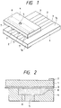
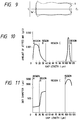
- Figures 1 and 2 show an ink jet recording head, which is a first embodiment of the invention.
- reference numeral 1 designates a piezoelectric body substrate, which is prepared by molding a PZT ceramic ("Nepeck N21 manufactured by Tokin) into a thickness of 600 ⁇ m and polarizing it thicknesswise so that it can vibrate in an edge mode.
- the edge-mode vibration is a state of vibration in which vibrational energy concentrates at end portions of a piezoelectric plate, and exhibits the feature that a higher degree of kinetic energy can be given to a substance that is in contact with the end portions with a small amount of drive energy.
- a common electrode 2 arranged by forming an electroconductive film that extends in parallel to an end surface 1a.
- each segment electrode 3 and common electrode 2 are prepared by sputtering two metal layers, one made of NiCr and the other made of Au, and then forming them into predetermined dimensions by, e.g., photolithography.
- the width of each segment electrode 3 and common electrode 2 is 150 ⁇ m, and the segment electrodes 3 are arrayed at an interval of about 254 ⁇ m.
- Reference numeral 4 designates an ink supply member.
- On a side confronting the piezoelectric body substrate when the ink supply member 4 is assembled into the piezoelectric body substrate 1 as a recording head is an ink tank 6 that serves to supply the ink from an ink supply inlet 5 to the segment electrodes 3, uniformly.
- the ink supply member 4 is also secured to the piezoelectric body substrate 1 so that ink mist jetting outlets 8 are formed at a portion confronting the end surface 1a of the piezoelectric body substrate 1 through spacers 7 that are disposed between the electrodes.
- Each ink mist jetting outlets 8 is formed so that a distance of about 5 to 30 ⁇ m is kept with respect to the corresponding segment electrode 3.
- Each space 7 is formed by sputtering an aluminum film of about 10 ⁇ m in thickness on a surface of a glass substrate of about 1 mm in thickness and then etching the aluminum thin film into a predetermined profile by photolithography, or the spacer is formed by coating microbead which has a diameter similar to that of the gap to be formed and which is mixed with an adhesive.
- the common electrode 2 is grounded and a segment electrode in a region to which the ink is jetted is selected, and an alternate voltage whose frequency is about 2 to 7 MHz is applied across the electrodes 2, 3.
- An alternate electric field acts only on a small region of the piezoelectric body substrate 1 interposed between the selected segment electrode 3 and the common electrode 2 to which drive signals have been applied.
- the region of the piezoelectric body substrate 1 on which the electric field acts i.e., only its edge portion, vibrates in synchronism with the frequency of the drive signal.
- the thus initiated vibration is such that its energy concentrates on an end portion at which the common electrode 2 of the piezoelectric body substrate 1 is formed; i.e., a so-called thickness edge-mode vibration produced by applying a predetermined drive signal frequency that is determined by the thickness of the piezoelectric body substrate 1 and a frequency coefficient for a thickness edge mode.
- the vibrational energy is transmitted to the ink that has been introduced to the ink mist jetting outlet 8 from the ink supply member 4 by capillary action.
- the vibration propagated to the ink is then converted into a surface wave at the interface with the air.
- the ink When the energy of the surface wave takes a value larger than a predetermined level, the ink is separated into small particles, misted and splashed a distance of about several millimeters in a predetermined direction, eventually forming a dot by adhering to a recording sheet arranged in front of the jetting outlet.
- Figure 3 shows dots formed by changing the time for which a drive alternate voltage is applied on a 100-microsecond basis between 100 and 500 microseconds using the head in the form of microphotography.
- the diffusion area of the ink mist is constant and its integrated amount is proportional to the time. Thus, it is understood that only the density of the dot is increased in proportion to the application time without changing the area.
- Figure 4 plots measurements of the optical density of a dot formed by extending the alternate voltage application time to 1 millisecond. It is found from these measurements that the optical density can be varied by the alternate voltage application time without changing the dot forming area over such a wide density range from about 0.1 to 1.8.
- the optical density of a dot can be changed minutely with such a simple operation as adjusting the drive voltage application time without changing the dot forming area. Therefore, a faithful recording of data including the tone data such as image data can be implemented without reducing the resolution.
- the sample used is a 600 ⁇ m-thick PZT ceramics (Nepeck N21 manufactured by Tokin) having such a vibrational characteristic as shown in Table 1.
- the PZT ceramics was similarly subjected to a polarization process in the direction of thickness and had the common electrode 2 and the segment electrodes 3 formed.
- a bias voltage Vb of 200 V is applied to the thus prepared sample, or the piezoelectric body substrate 1, in the direction of polarization so that the polarization is not inverted.
- Effective power to be supplied between the common electrode 2 and segment electrodes 3 of the piezoelectric vibrating body 1 was maintained at a constant value, only changing the frequency thereof.
- Figure 5 shows the results of the analysis.
- the curve designated by reference character a indicates a characteristic in the case where a sinusoidal wave such as shown in Figure 6 was used
- the curve designated by reference character b indicates a characteristic in the case where a rectangular wave such as shown in Figure 7 was used.
- the frequency coefficient in the case of jetting the ink is 1300 Hz - m when calculated from the thickness of the piezoelectric body substrate and the resonance frequency based on the results of the above analysis.
- the mode of vibration produced by the sample is either the longitudinal mode or the thickness edge mode, referencing the frequency constants classified by the vibrating mode in Table 1.
- the vibration produced by the sample is one of the aforesaid two modes, the maximum displacement observed on a segment electrode when a 600 ⁇ m-thick piezoelectric body substrate was driven at a frequency of 2.2 MHz was measured using a displacement gauge (Optical Probe manufactured by BMI). The obtained results are as shown in Figure 8.
- the horizontal axis in Figure 8 expresses the distance toward the segment electrode 3 on a ⁇ m basis with the end portion of the piezoelectric body substrate having the common electrode 2 as its origin, while the vertical axis expresses the amount of displacement at the small region at respective positions.
- the amplitude in the thickness direction becomes maximum at the edge portion, while the displacement at the center of the piezoelectric body substrate is significantly reduced.
- the piezoelectric body substrate vibrates in the thickness edge mode, in which, as shown in Figure 9, the edge portion 1a' vibrates with the maximum amplitude that is symmetrical about the centerline C-C, the edge portion 1a being in a region where the electrodes are formed.
- region A the gap length ranging from 5 to 20 ⁇ m is hereinafter referred to as "region A"
- region B the gap length raging from 20 to 40 ⁇ m
- region C the gap length raging from 40 to 100 ⁇ m is hereinafter referred to as "region C"
- region D the gap length ranging from 110 to 115 ⁇ m
- the relationship between the gap length and the diameter of a dot formed on a recording sheet was analyzed.
- the diameter of the dot formed on the recording sheet was about 200 ⁇ m with the size of the ink particles forming the mist being uniform.
- the diameter of the dot formed on the recording sheet exceeded 500 ⁇ m and the size of the individual ink particles became extremely inconsistent.
- the region D not only the diameter of the dot formed on the recording sheet became so large as 3000 to 5000 ⁇ m, but also the size of the individual ink particles increased, producing spots which make its optical density locally nonuniform.
- Figure 12 schematically shows these phenomena.
- the ink particles are produced at the ink mist jetting outlet in a predetermined direction, converged while maintaining this direction, and splashed onto a recording sheet.
- the ink particles are produced at the ink mist jetting outlet in a diverging direction and splashed while maintaining the diverging direction. In this case, some ink portions that are not sufficiently misted, i.e., ink droplets, are additionally produced, this making the diameter of the individual ink particles inconsistent.
- the ink at the ink mist jetting outlet is not misted although it is being vibrated.
- the ink while behaving as it does in the region C, is misted, producing some insufficiently misted particles, or ink droplets.
- the ink droplets are splashed while diverging at a large angle.
- the aforesaid piezoelectric body substrate produces optimal ink mist when the gap length of the ink mist jetting outlet is in the range of 5 to 20 ⁇ m, because with such gap length, the individual ink particles forming the ink mist have a consistent size and are splashed in a predetermined direction, allowing a small dot to be formed.
- the piezoelectric body substrate used in the above analyses was 600 ⁇ m in thickness. Similar analyses were made using a 200 ⁇ m-thick PZT ceramic piezoelectric body substrate. This piezoelectric body substrate initiated an edge-mode vibration at 6.6 MHz. The modes of the ink mist similarly produced by changing the gap length of the ink mist jetting outlet were studied.
- the obtained results indicate that a phenomenon similar to that in the region A was observed when the gap length of the ink mist jetting outlet was 7 ⁇ m or less; that the phenomenon in the region B was observed when the gap length ranged from 7 to 13 ⁇ m; and that the phenomenon in the region C was observed when the gap length ranged from 34 to 40 ⁇ m. That is, the same phenomena were observed with the gap length of the ink mist jetting outlet which was reduced by 1/3, in proportion to the 1/3 reduction in the thickness of the piezoelectric body substrate.
- Such a phenomenon will be further analyzed in relation to the wavelength of a vibration propagated to ink. Since aqueous ink is used in this analysis, the wavelength of a vibration produced in the ink present in the gap was 680 ⁇ m when the 600 ⁇ m-thick piezoelectric body substrate was used, and 230 ⁇ m when the 200 ⁇ m-thick piezoelectric body substrate was used (assuming that the sound speed of water is 1500 m/s).
- the phenomenon in the region A i.e., the phenomenon that the ink mist produced is converged, that the size of a dot formed is small, and in addition, that the size of the individual ink particles is small and consistent, occurs when the gap length of the edge portion of the piezoelectric body substrate is about 1/30 or less the wavelength of a vibration produced in the ink.
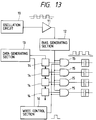
- Figure 13 shows an exemplary drive circuit suitable for operating an ink jet recording head of the invention.
- the drive circuit is constructed as follows.
- a 2.2-MHz signal from an oscillation circuit 10 is amplified to a power level appropriate for producing ink mist by an amplifier 11 and is biased to a polarizing voltage by a bias generating section 12.
- signals generated by a data generating section 13 are sequentially stored by shift registers 14 in correspondence with the positions of the segment electrodes 3.
- These two types of signals are inputted to AND gate circuits 15 and outputted to the segment electrodes 3 in synchronism with the input timing of a timing signal from a write control section 16.
- the drive signals are simultaneously applied to the respective segment electrodes at a plurality of dot forming regions in the above example. If the segment electrodes are arranged closer to one another to improve the resolution, then so-called crosstalk may, in some case, occur, the crosstalk being the phenomenon that a vibration is propagated between two adjacent segment electrodes and that dots are thereby formed on wrong positions.
- the segment electrodes may be divided into two rows, odd and even, and printing is performed by doubling a single dot forming time interval to Tb, with the first half time interval Tb/2 being used by the odd row and the latter half time interval Tb/2 being used by the even row.
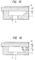
- segment electrodes 3 are arranged so as to come in contact with the ink in the above embodiment, it may be so arranged that the ink comes in contact with a common electrode 20 by inverting a piezoelectric body substrate 22 inside out as shown in Figure 15 and that a segment electrode 21 becomes the upper surface, whereby not only the width of the piezoelectric body substrate 22 can be set to a value closer to the width of the ink supply member compared with the above embodiment, but also the interconnections between the segment electrodes and the drive signal circuit can be simplified.
- Figure 16 shows another embodiment of the invention.
- reference numeral 25 designates a piezoelectric body substrate that is disposed so as to confront an electrode 20 arranged on an ink mist jetting outlet 8, e.g., the common electrode 20, while interposing a gap therebetween.
- the substrate 25 is so long as to cover the entire ink mist forming region.
- electrodes 25a and 25b formed to exert an alternate electric field on itself for driving.
- a drive signal is normally applied across the electrodes 25a, 25b of the piezoelectric body substrate 25, the drive signal being at a level low enough to jet no ink mist, so that the entire part of the piezoelectric body substrate 25 is being vibrated, whereby a surface wave having energy obtained immediately before producing ink mist to the ink at the ink mist jetting outlet is generated.
- a drive signal to a segment electrode with which to form a dot under this condition, the ink present in such segment electrode region is easily misted in response to the surface wave whose energy is extremely small.
- the energy required to mist the ink can be divided into two piezoelectric body substrates, thereby contributing to reducing the voltage level of a drive signal to be applied to a piezoelectric body substrate and thus allowing inexpensive, low voltage withstanding circuit parts to be used in the drive circuit.
- the signal to be applied to the piezoelectric body substrate 25 be a signal having such a frequency that the piezoelectric body substrate 25 initiates an edge-mode vibration.
- Figure 17 shows another exemplary ink mist jetting outlet.
- reference numeral 30 designates a slit that opens at one edge portion 31a of a piezoelectric body substrate 31.
- the slit 30 is about 10 ⁇ m wide and is subjected to a cutting process using a dicing saw so that it is deep enough to retain a sufficient amount of ink for misting, with a gap holding member 32 being inserted if necessary.
- the slit 30 communicates with ink supply inlets 33 bored on one of the surfaces of the piezoelectric body substrate 31, so that the ink can be supplied therefrom.
- a common electrode 34 is formed on the other surface of the piezoelectric body substrate 31 so as to interpose the slit 30, while segment electrodes 35 are formed so as to intersect the common electrode 34 while interposing the substrate 31 therebetween.
- the aforesaid ink holding member can be dispensed with, allowing the entire head to be made very thin.
- recording with a higher degree of density can be possible by laminating the dot forming regions of the respective piezoelectric body substrates while shifting by a predetermined pitch.
- the recording head can be down-sized.
- segment electrodes in the above embodiment is formed so as to be independent of one another by sputtering or photolithography, it may be so formed that as shown in Figure 18, an electroconductive layer is formed on one entire surface of a piezoelectric body substrate 40 by sputtering and is separated by grooves 41 so as to arrange segment electrodes 42.
- the grooves are formed using a dicing saw at such a pitch as to allow each projection to function as a segment electrode, each groove having a depth half the thickness of the piezoelectric body substrate 40 and extending to both edge portions thereof.
- a common electrode 43 is formed on one end of the thus prepared piezoelectric body substrate and an ink mist jetting outlet is formed on the common electrode 43 side. By supplying the ink to the ink mist jetting outlet, a recording head is completed.
- each of the segment electrodes 42 are separated by the grooves 41 so that propagation of a vibration produced at adjacent segment electrodes can be damped by the grooves.
- this not only allows the segment electrodes to be arrayed at a smaller pitch so that a recording head with a higher degree of density can be obtained, but also enables restriction of each vibrating region to be released by each groove 41 so that an adequate amount of ink mist can be produced even at a voltage that is lower compared with that applied when the segment electrodes are formed by patterning.
- interference in the vibration due to drive signals being out-of-phase with one another can be reduced, one of the drive signals being applied to adjacent segment electrodes simultaneously.
- the recording head can be safeguarded against breakage.
- a groove 47 is arranged on a surface opposite to the surface on which grooves 45, each separating segment electrodes 44 arranged on a piezoelectric body substrate 43a, are formed, i.e., on a surface on which a common electrode 46 is formed.
- the groove 47 intersects the grooves 45 for separating the segment electrodes 44 and is deep enough to be connected thereto. As a result, the grooves 45 communicate with the groove 47 at regions 48 where they overlap one upon the other.
- a slit plate 49 is arranged on the side of the segment electrodes 44 of the thus constructed piezoelectric body substrate 43a, the slit plate serving to form an ink mist jetting outlet. And when ink is supplied from the common electrode 46 side, the ink introduced into the groove 47 flows into the segment electrode 44 side from the region 48 where the groove 45 and the groove 47 intersect and is retained in a gap formed between the slit plate 49 and the segment electrode 44. Upon application of a drive signal to the segment electrode 44 under this condition, an edge-mode vibration is produced at the edge portion of the piezoelectric body substrate 43a hence misting the ink.
- Figure 20 shows still another embodiment of the invention.
- reference numeral 50 designates a piezoelectric body substrate, on both surfaces of which are segment electrodes 51 and a common electrode 53 formed, respectively.
- Reference numeral 52 designates an ink mist jetting outlet forming member disposed so as to confront the segment electrodes 51 of the piezoelectric body substrate 50.
- projections 51a At its regions confronting the segment electrodes 51 are projections 51a arranged to form intervals, each being so long as to produce ink mist, while at its regions confronting the portions between the segment electrodes are recesses arranged to form such gaps as not to produce the ink mist.
- Figure 21 shows another embodiment of the invention.
- reference numeral 55 designates a piezoelectric body substrate, on both surfaces of which are common electrodes 56, 57 formed so as to cover dot forming regions.
- Reference numerals 59 designate piezoelectric body substrates, each of which produces an edge-mode vibration. These substrates 59 are disposed so as to position at dot forming regions and maintain electroconductivity with one of the common electrodes 56 of the piezoelectric body substrate 55, while on the other surfaces of the substrates 59 are segment electrodes 60 formed.
- Reference numeral 58 designates an ink mist jetting outlet forming member disposed so as to maintain an appropriate ink mist forming interval with respect to the segment electrodes 60 of the piezoelectric body substrates 59.
- the vibration is propagated to the piezoelectric body substrates 59 so as to be imparted to the ink present between the segment electrodes 60 and the ink mist jetting outlet forming member 58.
- the piezoelectric body substrate 59 produces an edge-mode vibration, so that this vibrational energy is superposed on the ink that is receiving the vibrational energy from the piezoelectric body substrate 55.
- the ink at this region is misted and splashed toward a recording sheet.
- the piezoelectric body substrates 59 are disposed on the piezoelectric body substrate 55 at a pitch. Since the gap of a dot non-forming region is made larger than the gap of a dot forming region, there is no likelihood that the ink present in the former gap is misted, thereby preventing crosstalk from being caused.
- Figure 22 shows an exemplary ink mist jetting outlet forming member.
- reference numeral 62 designates an ink mist jetting outlet forming member disposed so as to confront a common electrode 64 that is formed at an edge portion of a piezoelectric body substrate 63.
- an ink mist forming region i.e., a region at which the common electrode 64 and segment electrodes 65 intersect, are V-shaped notches 62a formed, the notches having a maximum width W s and a depth of D t0 .
- the ink retained in the notches 62a by surface tension generates a surface wave while receiving the edge-mode vibration produced by the piezoelectric body substrate 63, thereby misting the ink.
- the splashing direction of the misted ink is restricted by the notches 62a of the ink mist jetting outlet forming member 62 which limit the opening to the air such as windows.
- the ink mist is in no other way than being splashed in an direction guided by the notches 62a.
- the presence of the notches 62a contributes to reducing the diffusion of the splashing ink mist compared with the case where they are absent, thereby allowing smaller dots to be printed.
- this embodiment can block splashing of the ink mist produced at dot non-forming regions, thereby allowing a high quality recording to be made.
- Figure 23 shows another exemplary ink mist jetting outlet forming member.
- reference numeral 66 designates an ink mist jetting outlet forming member disposed so as to confront the piezoelectric body substrate 63.
- Triangular projections 66a are formed in a region at an edge portion of the piezoelectric body substrate 63 at which the common electrode 64 and the segment electrodes 65 intersect, each projection having a width of W t1 and a depth of D t1 .
- the ink present between the ink mist jetting outlet forming member 66 and the piezoelectric body substrate 63 moves only toward the farther region at which the common electrode 64 and the segment electrodes 65 intersect by surface tension relative to the triangular projections 66a.
- an edge-mode vibration produced at this region acts upon the ink retained in the triangular projections 66a, thereby misting the ink.
- no ink is misted from the triangular projections 66a, because no is present in the triangular projections, thereby totally preventing crosstalk.
- Figure 24 shows another exemplary ink mist jetting outlet.
- reference numeral 68 designates a first regulating member, one end of which is disposed so as to position at a region at which the common electrode 64 and the segment electrodes 65 formed on the piezoelectric body substrate 63 intersect
- reference numeral 69 designates a second regulating member, one end of which is disposed in a vibrating region W c while keeping a gap D t2 that forms a desired diameter of a dot with respect to the first regulating member 68.
- the ink when ink is supplied to the first regulating member 68 that serves both as an ink supply member, the ink is retained at an edge portion of the first regulating member 68 by capillary action generated between the piezoelectric body substrate 63 and the first regulating member 68.
- the ink retained at the edge of the first regulating member is misted and is about to be splashed outside.
- the second regulating member 69 is blocking the opening for splashing, part of the produced mist cannot splash. As a result, a dot whose diameter is appropriate for printing can be formed.
- Figures 25 (a) and (b) show the structure of a common electrode at an ink mist forming region.
- reference numeral 70 designates a hornlike projection formed at a vibrating region at which a common electrode 71 and segment electrodes 72 intersect. This projection is formed by thick-film printing using a type of paint which exhibits a high degree of density when dried, such as silver paste whose viscosity is reduced by a solvent.
- the edge-mode vibration produced at a piezoelectric body substrate 73 since the edge-mode vibration produced at a piezoelectric body substrate 73 has an extremely short wavelength, its vibrational energy concentrates at the apex of the hornlike projection 70. As a result, the ink retained between the piezoelectric body substrate 73 and a not shown ink mist jetting outlet forming member receives a high level of energy from such a limited region as the apex of the hornlike projection 70, causing ink particles, each having an extremely small diameter, to splash at a high velocity in the form of mist. As a result, a dot whose diameter is small can be formed on a recording sheet.
- hornlike projection 70 is prepared by the silver paste in this embodiment
- a hornlike projection 75 having a similar function may be used, the projecting 75 being formed by superposing circular metal films 74a, 74b, 74c, 74d, ..., whose diameters are gradually reduced, respectively, on upon the other by sputtering, as shown in Figures 26 (a) and (b).
- Figure 27 shows another exemplary common electrode 71 at an ink mist forming region.
- reference numeral 76 designates a recess formed on a surface of the common electrode 71.
- the recess is formed by laminating a plurality of layers consisting of annular metal patterns 77a, 77b, 77c, 77d, ..., whose holes in the center are gradually increased, respectively, by sputtering.
- the ink transferred from a not shown ink supply member to the common electrode 71 enters the recess 76 by surface tension.
- a drive signal to the segment electrode 72 with which to form a dot under this condition an edge-mode vibration is produced at the piezoelectric body substrate 73, and this vibration is converged toward the center of the recess 76 by the surrounding wall surface of the recess 76, imparting a high degree of vibrational energy to the ink retained there.
- the ink is misted in response to the high level of vibrational energy, splashing outside with its splashing direction being restricted by the wall surface of the recess 76.
- a dot whose diameter is small can be printed on a recording sheet.
- the recess is constructed by forming the annular metal patterns on the surface of the common electrode 71 in this embodiment, it goes without saying that a similar function may be obtained by a recess 78 formed on the piezoelectric body substrate 73 while, e.g, etching the recesses 77a, 77b, 77c, 77d, ... whose radii are gradually reduced, respectively.
- the mass of the vibrating region does not change, thereby allowing the edge-mode vibration to be produced stably.
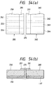
- Figures 29 (a) and (b) show a exemplary structure of the common electrode and segment electrodes forming a piezoelectric body substrate that has been developed to meet the aforesaid requirements.
- reference numeral 80 designates a piezoelectric body substrate appropriate for producing an edge-mode vibration, whose thickness h is, e.g., about 200 to 600 ⁇ m.
- Reference numeral 81 designates a common electrode formed on an edge portion on one of the surfaces of the piezoelectric body substrate 80. Its width W is set to a value one half the thickness h of the piezoelectric body substrate 80.
- Reference numerals 82 designate segment electrodes formed on the edge portion of the other surface of the piezoelectric body substrate 80.
- the segment electrodes confronting the common electrode 81 is formed into a width W' that is, in a similar manner, one half the thickness h of the piezoelectric body substrate 80 and is arrayed at such a pitch as to coincide with a single dot length.
- One end of lead patterns 82a is connected to the segment electrodes 82, respectively, the width of each lead pattern being set to a value extremely smaller than that of the segment electrode.
- drive signals applied from an external drive circuit act on the segment electrodes 82 via the lead patterns 82a, causing an electric field to exert on an area h/2 from the edge portion of the piezoelectric body substrate 80.
- This causes the piezoelectric body substrate 80 to vibrate in the edge mode only at the region 1/2 its thickness from its edge, allowing the power applied to the electrodes 81, 82 to be effectively utilized to produce ink mist.
- the lead patterns 82a are narrow and that the common electrode 81 opposite to them is not present. Thus, there is no likelihood of consuming power uselessly at this region.
- the widths W, W' of the common electrode 81 and the segment electrode 82 can initiate no vibration adequate to produce ink mist at the edge portion of the piezoelectric body substrate 80, while the widths W, W' taking values 70% or more can produce vibrations even at regions not having to do with ink mist production, thereby not only wasting power but also making it likely to increase crosstalk. Therefore, the optimal widths of the common electrode 81 and the segment electrode 82 range from 30 to 70% the thickness h of the piezoelectric body substrate 80 from the standpoint of ink mist producing efficiency, power utilization, and crosstalk prevention.
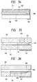
- Figure 31 (a) shows an embodiment contrived to prevent the formation of water drops.
- reference numerals 91, 92 designate films formed on respective edge portions of the piezoelectric body substrate 85 and the ink mist jetting outlet forming member 86 which form the ink mist jetting outlet 93.
- a lipophilic material is selected, while in the case of water-color ink, a hydrophilic material is selected.
- the films are formed by coating or the like.
- reference numeral 98 designates a common electrode ; and 99 designate segment electrodes, both formed on the piezoelectric body substrate 85.
- the ink mist jetting outlet 93 that is formed between the piezoelectric body substrate 85 and the ink mist jetting outlet forming member 86 which also serves for ink supply, becomes stagnant due to stoppage of printing, the ink tends to form a water drop over the front end of the jetting outlet 93 by surface tension.
- the lipophilic or hydrophilic films 91, 92 formed on the respective surfaces of the piezoelectric body substrate 85 and the ink mist jetting outlet forming member 86 causes the ink to be diffused in the formed of layers 94, 95 along the films 91, 92 as shown in Figure 31 (b), thereby allowing no water drop to be formed.
- the ink mist is produced stably.
- the ink mist jetting outlet 93 being kept moistened at all times by the solvent of the ink absorbed by the porous bodies 96, 97, is protected from being dried as much as possible, thereby allowing printing to be performed smoothly. While it is both the piezoelectric body substrate 85 and the ink mist jetting outlet forming member 86 that are coated or provided with the porous bodies in the above embodiments, it goes without saying that it may instead be only one of them that is coated or provided to obtain a similar effect.
- the magnetic ink retained at the ink mist jetting outlet 101 receives an edge-mode vibration from a piezoelectric body substrate 104 and the superfine magnetic particles forming the ink are misted together with the solvent and splashed toward the recording sheet 102.
- the misted superfine magnetic particles reach the recording sheet 102 while accelerated in response to the magnetically attracting force from the magnet 103 in the course of splash. Accordingly, the ink particles, once misted, are no longer diffused, reach and adhere to the recording sheet without fail. Further, since the ink, once misted, splashes toward the recording sheet by the magnetically attracting force, it needs only few splashing energy from the piezoelectric body substrate.
- the drive power to be supplied to the piezoelectric body substrate 104 can be reduced, which in turn contributes to low-voltage drive of the drive circuit.
- the ink is accommodated in a space formed between the ink supply member and the piezoelectric body substrate in the above embodiments, it may be so arranged that the ink is retained at the ink retaining member formed, e.g., by a porous body and that the ink is supplied therefrom to the ink misting region.
- Figure 34 shows an exemplary recording head using a porous body as an ink retaining member.
- reference numeral 105 designates a piezoelectric body substrate, at the edge portion of which are not only segment electrodes 106 and a common electrode 107, but also an ink mist jetting outlet 109 formed by a case 108.
- Reference numeral 110 designates a porous body accommodated within the case 108, the porous body serving to absorb and retain ink from an ink supply inlet 111.
- the ink introduced from the ink supply inlet 111 is temporarily absorbed by the porous body 110 and retained by its surface tension.
- the piezoelectric body 105 produces an edge-mode vibration.
- the ink absorbed by the porous body 110 is oozed into the ink mist jetting outlet 109 in response to the vibration, misted at the outlet 109, and splashed outside.
- the vibration is no longer exerted on the porous body 110 as the drive signal stops, the ink that is no longer misted and remains at the ink mist jetting outlet 109 is absorbed by the porous body 110 again.
- the formation of a water drop over the surface of the ink mist jetting outlet 109 by the ink during stoppage can be prevented, allowing stable printing to be implemented.
- Figure 35 shows another embodiment of the invention.
- reference numeral 115 designates a piezoelectric body substrate having a common electrode 116 and segment electrodes 117 and being polarized thicknesswise. On one of its surfaces is an ink retaining member 119 provided through a space 118, forming an ink mist jetting outlet 120 at an edge portion of the piezoelectric body 115.
- Reference numeral 121 designates a wedge member provided either on the piezoelectric body substrate 115 or the ink retaining member 119; it is provided on the ink mist jetting outlet side of the ink retaining member 119 in this embodiment. It is arranged so as to come in resilient contact with the segment electrode 117 at all times to such an extent that the flow of the ink into the ink mist jetting outlet 120 is prevented.
- the ink introduced from an ink supply inlet 122 is retained in a space formed between the ink retaining member 119 and the piezoelectric body substrate 115 with its flow into the ink mist jetting outlet 120 being blocked by the wedge member 121.
- the piezoelectric body substrate 115 Upon application of a drive signal to the segment electrode 117 with which to form a dot under this condition, the piezoelectric body substrate 115 produces an edge-mode vibration.
- the vibration causes a gap to be formed intermittently between the wedge member 121 and the segment electrode 117, and the ink retained in the space between the ink retaining member 119 and the piezoelectric body substrate 115 moves to the ink mist jetting outlet 120 while following this gap.
- the ink that has reached the gap is misted in response to the edge-mode vibration from the piezoelectric body substrate 115 and splashed toward a recording sheet.
- the wedge member 121 blocks the flow path of the ink to the ink mist jetting outlet 120 while brought into resilient contact with the segment electrode 117.
- the ink solvent is no longer dried nor clogs the outlet because of its being shielded from the air by the wedge member 121.
- Figure 36 shows another embodiment using a principle similar to that shown in Figure 35.
- reference numeral 125 designates a piezoelectric body substrate having a groove 127 that extends to a position immediately before an ink mist jetting outlet 126. Segment electrodes 128 are formed so as to extend to a position appropriate to be connected to an external drive circuit via this groove 127 from the ink mist jetting outlet 126.
- Reference numeral 129 designates a spacer member which not only has a thickness appropriate for forming the ink mist jetting outlet 126 at an edge portion of the piezoelectric body substrate 125, but also is secured to both the piezoelectric body substrate 125 and an ink mist jetting outlet forming member 130 only at a position on the rear end side (at "left” in Figure 36) so that the ink mist jetting outlet 126 comes in resilient contact with the front end of the groove 127 of the piezoelectric body substrate 125.
- the ink supplied from an ink supply inlet 131 moves toward the vicinity of the ink mist jetting outlet 126 via the groove 127 that is formed on the piezoelectric body substrate 125. Since the spacer member 129 closes the front end portion of the groove 127 when no drive signal is applied to the piezoelectric body substrate, the ink is not admitted to the ink mist jetting outlet 126. Upon application of a drive signal under this condition, the piezoelectric body substrate 125 produces an edge-mode vibration. As a result, a gap is formed intermittently between the spacer member 129 and the segment electrode 128, causing the ink to follow the gap to move into the ink mist jetting outlet 126. The ink that has reached the ink mist jetting outlet 126 is misted in response to the edge-mode vibration from the piezoelectric body substrate 125 and splashed toward a recording sheet.
- the spacer member 129 closes the front end portion of the groove 127 formed on the piezoelectric body substrate 125 so that the application of the ink supplied to the ink mist is stopped.
- the ink is no longer misted uselessly with crosstalk from the adjacent segment electrodes, but also the ink solvent is not clogged.
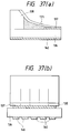
- Figures 37 (a) and (b) show another embodiment of the invention.
- reference numeral 135 designates an ink mist jetting outlet forming member made of a plate spring member. It is arranged on a piezoelectric body substrate 136 through a fixing member 138 so that one end of the member 135 comes in resilient contact with a common electrode 137 of the piezoelectric body substrate 136.
- Reference numerals 140 designate segment electrodes disposed on the piezoelectric body substrate 136.
- the ink when ink is loaded to a space 139 formed between the piezoelectric body substrate 136 and the ink mist jetting outlet forming member 135, the ink moves to a front end gap formed between the common electrode 137 and the ink mist jetting outlet forming member 135 by surface tension. Since the ink is shielded from the air by the ink mist jetting outlet forming member 135 under this condition, evaporation of the solvent composing the ink is suppressed, thereby preventing clogging of the gap.
- the piezoelectric body substrate 136 Upon application of a drive voltage to the segment electrode 140 with which to form a dot under this condition, the piezoelectric body substrate 136 produces an edge-mode vibration, forming the gap between the common electrode 137 and the ink mist jetting outlet forming member 135. As a result, the ink flowing into the gap generates a surface wave in response to the edge-mode vibration from the piezoelectric body substrate 136, the ink further being misted and splashed outside.
- cuts may be provided by the dot forming region as indicated by the one dot chain lines in Figure 37 (b), so that crosstalk from adjacent segment electrodes can be prevented.
- ink mist jetting outlet forming member is arranged so as to come in contact with the common electrode in this embodiment, it goes without saying that a similar effect may be obtained by causing the ink mist jetting outlet forming member to come in contact with the segment electrodes.
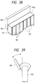
- Figure 38 shows an exemplary piezoelectric body substrate of the invention.
- reference numeral 145 designates a piezoelectric body substrate for producing an edge-mode vibration. On one of its surfaces is a common electrode 146, while on the other surface are segment electrodes 147 formed. The substrate 145 is also polarized thicknesswise.
- Reference numeral 148 designates a vibration amplifying plate, which is a thin plate secured to the piezoelectric body substrate 145 by protruding from an edge portion 145a of the piezoelectric body substrate 145, the thin plate being extremely thin compared with the thickness of the piezoelectric body substrate 145.
- an ink mist jetting outlet forming member is disposed so as to confront the vibration amplifying plate 148 as described before, and a drive signal is applied to the segment electrode 147 with the ink retained by a gap formed between the vibration amplifying plate 148 and the ink mist jetting outlet forming member.
- the piezoelectric body substrate 145 similarly produces an edge-mode vibration. Since the vibration produced by the piezoelectric body substrate 145 exhibits the maximum amplitude at the edge, the vibration amplifying plate 148 is subjected to rotational vibration around a single point as shown in Figure 39, and the amplitude of the front end of the vibration amplifying plate 148 becomes larger than that of the end portion of the piezoelectric body substrate 145.
- the ink present between the ink mist jetting outlet forming member and the vibrating amplifying plate 148 receives a vibration whose amplitude is larger than that produced by the piezoelectric body substrate 145, thereby being misted at a higher efficiency.
- Figure 40 shows another exemplary vibration amplifying plate
- reference numeral 150 designates a vibration amplifying plate similarly secured to the edge portion 145a of the piezoelectric body substrate 145.
- V-shaped recesses 150a formed at positions confronting the segment electrodes 147.
- the ink mist jetting outlet forming member is similarly disposed so as to confront the vibration amplifying plate 148, and when ink is loaded to a gap formed therebetween, the ink enters the recesses 150a by surface tension and retained there.
- the piezoelectric body substrate 145 Upon application of a drive signal to the segment electrode 147 with which to form a dot under this condition, the piezoelectric body substrate 145 produces an edge-mode vibration. Since the vibration causes the front end of the vibration amplifying plate 148 to vibrate at a maximum amplitude, the ink retained at the recesses 150a are misted.
- the ink receiving the vibration is limited only to that retained at the recesses 150a, thus preventing the ink mist from being diffused.
- Figure 41 shows another exemplary vibration amplifying plate.
- reference numeral 153 designates a piezoelectric body substrate
- a vibration amplifying section 153a is formed on a front end of piezoelectric body substrate 153 by providing a step 153b by, e.g., etching.
- a common electrode 154 formed, while on the other surface thereof are segment electrodes 155 formed, so that an edge-mode vibration is induced close to the step 153b.
- an ink mist jetting outlet forming member is similarly disposed so as to confront the vibration amplifying section 153a, and ink is retained at a gap formed therebetween.
- an edge-mode vibration is produced close to the step 153b. Since this vibration is propagated to the vibration amplifying section 153a arranged at the front end of the piezoelectric body substrate 153 and has its amplitude amplified, thereby the ink is caused to be misted at a higher efficiency.
- the work of assembling the amplifying plate into the piezoelectric body substrate can be dispensed with, thereby contributing not only to streamlining the fabrication process but also to forming the amplifying plate without substantially increasing the mass of the vibrating region.
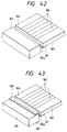
- reference numeral 160 designates a piezoelectric body substrate, on one surface of which is a common electrode 161, while on the other surface of which are segment electrodes 162 so as to intersect the common electrode 161.
- the substrate 160 is polarized thicknesswise.
- a gap forming member 164 On its front end portion 160a is a gap forming member 164 arranged so that a gap 163 appropriate for producing ink mist is provided.
- ink is supplied by a not shown ink supply member to the gap 163 formed between the front end portion 160a of the piezoelectric body substrate 160 and the gap forming member 164 and is retained in the gap 163 by capillary action.
- a drive signal to the segment electrode 162 with which to form a dot under this condition, an edge-mode vibration produced at the front end portion 160a of the piezoelectric body substrate 160 is transmitted to the ink, thereby generating a surface wave at the interface between the ink and the air, misting the ink, and splashing the misted ink in a predetermined direction.
- the front end portion 160a of the piezoelectric body substrate 160 and a piezoelectric body substrate 165 that can vibrate in an edge mode are disposed so as to form a gap 166 appropriate for producing ink mist, and electrodes 167, 168 are formed on both surfaces of the substrate 165 so as to be on the side of the gap 166.
- a vibration that is not large enough to mist the ink retained in the gap is similarly applied to the piezoelectric body substrate 165 at all times, whereby upon application of a comparatively small drive signal to the segment electrode 162, the ink can be misted selectively.
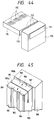
- Figure 44 shows another embodiment of the invention.
- reference numeral 170 designates a piezoelectric body substrate.
- On a front end portion of one of its surfaces is a common electrode 171 formed, while on the other surface are segment electrodes 172.
- the substrate 170 is also polarized thicknesswise.
- on one of its surfaces i.e., the surface having the segment electrodes 172 is a piezoelectric body substrate 174 formed.
- the substrate 174 is arranged adjacent to the front end portion while providing a gap 173 appropriate for producing ink mist therefrom.
- On a surface of the piezoelectric body substrate 174 are comb-like electrodes 175 arranged so as to confront the segment electrodes 172.
- ink is supplied to the gap 173 from a not shown ink supply member and the ascending level of the ink is limited to the lower end of the gap 173.
- an alternate signal is applied, the alternate signal having such a frequency that the piezoelectric body substrate 174 produces a surface wave to the comb-like electrode 175 confronting the segment electrode 172 with which to form a dot, and the frequency being, e.g., about 20 MHz. Accordingly, the surface wave moving from the comb-like electrode 175 to the segment electrode 172 is produced, causing the ink at the lower end of the gap 173 to ascend to the surface of the segment electrode 172.
- the edge portion of the piezoelectric body substrate 170 produces an edge-mode vibration, and the vibration, acting on the ink ascending along the segment electrode 172, mists the ink.
- the ink ascending along the segment electrode 172 descends to the lower end of the gap 173.
- Figure 45 shows another embodiment of the invention.
- reference numeral 180 designates a piezoelectric body substrate having a slit formed at the center thicknesswise.
- the slit has a depth equal to the width of a common electrode that is necessary to initiate an edge-mode vibration from the front end surface of an edge portion of the piezoelectric body substrate 180.
- a common electrode 181 is formed by embedding a conductor in this slit.
- the piezoelectric body substrate 180 is divided into two layers 180a, 180b demarcated by the common electrode 181. These layers 180a, 180b are polarized so as to oppose each other as indicated by the arrow in Figure 45.
- On both surfaces of the piezoelectric body substrate 180 are segment electrodes 182, 183, 184, ..., and segment electrodes 185, 186, 187, ... so as to confront one another.
- an ink mist jetting outlet forming member 188 is disposed on the segment electrodes 185, 186, 187, ... side so as to confront the piezoelectric body substrate 180 to form a gap appropriate for producing ink mist and retain the ink in this gap.
- the layers 180a, 180b of the piezoelectric body substrate 180 Upon application of a drive signal across the segment electrodes 183, 186 at the dot forming position and the common electrode 181, the layers 180a, 180b of the piezoelectric body substrate 180 produce an edge-mode vibration as if the electrodes were arranged on both surfaces of a single piezoelectric body substrate because a region interposed between the segment electrode 183 and the common electrode 181 and a region interposed between the segment electrode 186 and the common electrode 181 are subjected to alternate electric fields whose phases are opposite to each other. The thus produced vibration is transmitted to the ink retained in the gap and causes the ink to be misted.
- the piezoelectric body substrate 180 receives the electric fields by dividing itself into two portions thicknesswise, the voltage level to be applied to the common electrode 181 and the segment electrodes 182 to 187 can be reduced to 1/2 to obtain an electric field intensity necessary for producing ink mist. This contributes to implementing an inexpensive drive circuit.
- Figures 46 (a) and (b) show another exemplary piezoelectric body substrate of the invention.
- reference numerals 190 designate throughholes, each having a rectangular section, bored in a piezoelectric body substrate 191 in correspondence with each dot forming position.
- the throughholes are arranged at an equal interval in a row and a plurality of rows of throughholes are staggered from one to the other at an appropriate pitch, e.g., by half of the interval.
- the staggered pitch provides the advantage that the distance between dots to be printed can be reduced.
- Each of partitions 192 partitioning two adjacent throughholes 190 has its thickness selected so that an edge-mode vibration is induced, and it is polarized thicknesswise.
- On the surfaces of each partition 192 are electrodes formed as shown in Figure 46 (b) so that each partition 192 can produce an edge-mode vibration.
- Figure 47 shows another exemplary piezoelectric body substrate suitable for use in an ink jet recording head of the invention.
- reference numeral 195 designates a piezoelectric body block cut into a prism.
- On one surface thereof are equidistantly arranged grooves 196 to form a plurality of comb-like projections 197.
- the thickness of each projection 197 is so selected as to produce an edge-mode vibration.
- Each projection 197 is subjected to a polarization process in the direction of the adjacent recess.
- electrodes 198, 199 formed by, e.g., electroless plating.
- the ink When the thus constructed vibrating element block is immersed into a container or the like containing ink, the ink is retained in the grooves.
- the electrodes 198, 199 formed on both surfaces of the projection with which to form a dot the projection produces an edge-mode vibration, misting the ink retained in the groove and splashing the misted ink outside.
- Figure 48 shows another exemplary vibrating element assembly.
- reference numerals 200 designate piezoelectric body substrates, each being suitable for producing an edge-mode vibration and polarized thicknesswise.
- electrodes 201, 202 On both surfaces of each substrate 200 are electrodes 201, 202 arranged to form a vibrating element 203.
- These vibrating elements 203 are formed into a vibrating element assembly so that a plurality of vibrating elements 203 are adhesively fixed in a row at one end through spacers 205 interposed therebetween, respectively, each spacer providing a gap 204 appropriate for misting the ink.
- the piezoelectric body substrate 200 produces an edge-mode vibration, thereby misting the ink in the gap 204 and splashing the misted ink outside.
- Figures 49 (a) and (b) show another exemplary ink jet recording head of the invention.
- reference numeral 210 designates a piezoelectric body substrate that is polarized thicknesswise. On one of its surfaces are a plurality of parallelly extending recesses 212 formed while divided by partitions 211. Each recess 212 has an opening at one end. The thickness of a part of the piezoelectric body substrate having these recesses formed is selected to be a value appropriate to vibrate in an edge mode. On the other surface of the piezoelectric body substrate 210 are recesses for depositing the ink so as to load these recesses 212 with the ink.
- segment electrodes 215 formed while arranging electroconductive layers by sputtering, electroless plating, or the like.
- a common electrode 216 extending adjacent to the opening of each recess 212.
- reference numeral 218 designates an ink supply inlet.
- the ink moves from a recess 213 to the recesses 212 by surface tension, reaching their opening.
- a drive signal to the segment electrode 215 with which to form a dot under this condition Upon application of a drive signal to the segment electrode 215 with which to form a dot under this condition, a part of the piezoelectric body substrate constituting the bottom of the recess 212 vibrates in an edge-mode, misting the ink retained at the recess 212 above and splashing the misted ink outside.
- the whole body including the recess for depositing the ink is made up of the piezoelectric body substrate in this embodiment, it goes without saying that a similar effect may be obtained by forming only the common electrode and the segment electrodes on the piezoelectric body substrate while forming other portions including the ink depositing recess with a polymer, and by adhesively integrating these two parts.
- each segment electrode is formed in each recess 212 of the piezoelectric body substrate 210 in this embodiment, it goes without saying that a similar effect may be obtained by forming a common electrode 220 so as to traverse the recesses 212 and the partitions 211 as shown in Figure 50, and by arranging segment electrodes 221 on the other surface of the piezoelectric body substrate 210 so as to confront the recesses 212.
- Figures 51 (a) and (b) show another embodiment of the invention.
- reference numeral 225 designates a piezoelectric body substrate, on one surface of which are recesses 226 formed so as to correspond to dot forming regions, extending from one end to the other at a single depth as shown in Figure 51 (b). Pairs of segment electrodes 227a, 227b are formed so as to interpose the respective recesses therebetween.
- These drive electrodes may also be arranged by first forming a continuous electroconductive pattern that can cover an area to form the recesses, and then forming grooves in the middle thereof using a dicing saw.
- a common electrode 228 At one edge portion on the other surface of the piezoelectric body substrate 225 is a common electrode 228 formed.
- reference numeral 229 designates a member for forming an ink deposit at the other edge portion of the piezoelectric body substrate 225.
- This member is formed by, e.g., injection-molding a synthetic resin material and fixed using an adhesive.
- a substrate is fixed on the opening side of the recesses 226 and the ink deposit 229 on the piezoelectric body substrate 225 so that the opening can be sealed, and the ink is loaded to the ink deposit.
- the region at which the segment electrodes 227a, 227b are formed produces an edge-mode vibration.
- the vibration that is produced so as to interpose the recess 226 is propagated to the recess and causes the ink retained in the recess to be misted and splashed outside.
- a boat-like groove whose depth becomes shallower toward the ink mist producing side 230 as shown in Figure 51 (c) may be formed so as to prevent diffusion of the ink mist.
- Figure 52 shows another exemplary piezoelectric body substrate suitable for use in an ink jet recording head of the invention.
- reference numeral 235 designates a piezoelectric body substrate, on one edge portion of which is a front end portion 235a that is the deepest portion and on the other edge portion of which are recesses 236 connected to the surface of the substrate 235, each recess being formed so as to correspond a dot forming region.
- the thickness of the piezoelectric body substrate 235 at its front end is set to a value appropriate to vibrate in an edge-mode.
- On the bottom of each recess 236 is a segment electrode 237 formed as shown in Figure 53, which electrode in extended by a lead 238 to a position so as to be properly connected to an external signal source.
- reference numeral 239 designates a substrate for sealing the opening of each recess 236.
- a groove 240 formed, the groove having a length extending from a position confronting a part of the recess 236 to a position appropriate to supply ink so that the ink can be supplied from an ink supply inlet 241 to the recess 236.
- reference numeral 242 designates a common electrode formed so as to confront the recess 236 of the piezoelectric body substrate 235.
- the ink supplied from the ink supply inlet 241 in this embodiment flows into the recess 236 of the piezoelectric body substrate 235 via the groove 240 of the substrate 239, and retained by surface tension in the recess 236.
- the bottom surface of the recess 236 vibrates in an edge mode. This vibration is propagated to the ink retained in the recess 236, misting the ink there and splashing the misted ink outside.
- edge-mode vibrating elements 255, 265 are so arranged that on one surfaces of piezoelectric body substrates 250, 260 are common electrodes 251, 261 formed, respectively, while on the other surfaces thereof are segment electrodes 252, 253, 254, ... and 262, 263, 264, ... formed, respectively.
- a recording head is constructed by disposing such edge-mode vibrating elements 255, 265 so that their front end surfaces carrying the common electrodes 251, 261 confront each other to form a gap 270 appropriate for producing ink mist.
- each vibrating element e.g., the surface carrying the drive electrode
- the ink is retained in the gap 270 by surface tension.
- drive signals that are 180°-out-of-phase to each other but have the same level are applied to the segment electrodes 252, 253, 254, ... and 262, 263, 264, ... of the respective vibrating elements 255, 265.
- the edge-mode vibrations produced at the front end portions of the confronting vibrating elements 255, 265, being 180°-out-of-phase to each other under this condition, cancel each other out, thereby not misting the ink.
- the phase of the drive signal applied to one of these segment electrodes 253, 263, e.g., the segment electrode 253, is inverted. Accordingly, these electrodes 253, 263 receive the drive signals whose phases are the same, and this allows the piezoelectric body substrates 250, 260 at the regions of the electrodes 253, 263 to produce edge-mode structural vibrations of the same phase, thereby misting the ink retained at these regions and splashing the misted ink outside.
- the ink retained at regions adjacent to these electrodes 253, 263 and not contributing to forming the dot still receives the vibrations that are 180°-out-of-phase to each other from the piezoelectric body substrates 250, 260, thereby cancelling each vibrational energy out and not misting the ink.
- the vibrational energy from the two vibrating elements 255, 265 can be given to the ink retained in the gap 270 while superposed at the time the dot is being formed.
- the vibrational energy required for each vibrating element for misting the ink may be about half that of the aforesaid constructions with a single vibrating element, thereby contributing to implementing an inexpensive drive signal generating circuit.
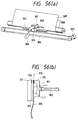
- Figures 55 (a) and (b) show another exemplary recording head having the aforesaid valve mechanism.
- reference numeral 280 designates a vibrating element in which electrodes 282, 283 are formed on both surfaces of a piezoelectric body substrate and this vibrating element produces an edge-mode vibration.
- the vibrating element 280 is secured to the opening of an ink tank 284 so that one side thereof confronts a recording sheet and the other side thereof comes in contact with ink 285 in the ink tank 284.
- Reference numeral 286 designates a slit forming member disposed at an end portion of the opening of the ink tank 284 so as to form a gap 287 appropriate for misting the ink by the vibrating element 280 interposed between the electrodes 283.
- Reference numeral 288 designates a bimorph piezoelectric element, one end of which gets curved by the application of a voltage. Its free end 288a is in resilient contact with the gap 287 at all times and the other end 288b is secured to the tank 284 so that the ink is blocked from entering into the gap 287.
- the vibrating element 280 receives an alternate voltage whose frequency is appropriate for producing an edge-mode vibration at all times. Since the gap 287 is closed by the end portion 288a of the bimorph piezoelectric element 288 when no drive signal is received, the ink is not admitted to the gap 287, thereby producing no ink mist.
- the end portion 288a of the bimorph piezoelectric element 288 gets curved toward the tank side to cause the gap 287 to communicate with the ink tank 284 ( Figure 55 (b)), thereby allowing the ink to be admitted to the gap 287.
- the ink introduced into the gap 287 is misted and splashed outside in response to the edge-mode vibration from the vibrating element 280 to form a dot on a recording sheet.
- the drive voltage is applied to the vibrating element 280 at all times and to apply a signal whose voltage level is large enough to drive the bimorph piezoelectric element 288 only when a dot is being formed.
- the drive signal having a high frequency and a comparatively high voltage, thereby not only allowing the drive circuit to be simplified in structure, but also preventing the clogging of the gap by keeping the ink solvent from evaporating while shutting the gap, which is an ink mist jetting outlet, from the ink in the ink tank by the bimorph piezoelectric element when no printing is performed.
- the piezoelectric body substrate is made of a PZT ceramic in the above embodiments. If lithium niobate (LiNbO3) or the like whose polarization breakage voltage is high is used, no bias voltage is necessary, thereby contributing to simplifying the drive circuit. It goes without saying that piezoelectric materials made of polymers, such as polyvinylidene fluoride film (PVDF), may be used.
- PVDF polyvinylidene fluoride film
- a piezoelectric body substrate having a shape suitable for producing ink mist can be fabricated by injection molding, thereby not only contributing to streamlining the fabrication process, but also improving the reliability of a recording head since such piezoelectric body substrate is highly resistant to brittle fracture.
- Figure 56 (a) and (b) shows one example of an ink jet printer including a ink jet recording head as modified to the ink jet recording head shown in Fig 1.
- a recording paper 309 supported by a platen 308 moves in a longitudinal direction.
- the ink jet recording head 301 is disposed on a carriage 303 fixed on the carriage conveyance belt 305 which is driven by the carriage conveyance motor 307, and the carriage 303 is slidably engaged with a carriage guide 304.
- the ink jet recording head is derived in the horizontal direction.
- the ink jet recording head 301 includes a piezoelectric body substrate 312 having electrodes 314 and 315, which is supported by a support substrate 311, an ink supply member 313 communicated with the ink supply tube 302, a flexible circuit 306 connected to the electrode 315 which is disposed to confront the ink supply member 313, and a ink mist 310 formed between an end portion of the ink supply member 313 and the electrode 315.
Landscapes
- Particle Formation And Scattering Control In Inkjet Printers (AREA)
- Ink Jet (AREA)
Applications Claiming Priority (12)
| Application Number | Priority Date | Filing Date | Title |
|---|---|---|---|
| JP267624/90 | 1990-10-05 | ||
| JP26762490 | 1990-10-05 | ||
| JP290418/90 | 1990-10-26 | ||
| JP29041890 | 1990-10-26 | ||
| JP29768090 | 1990-11-02 | ||
| JP297680/90 | 1990-11-02 | ||
| JP310514/90 | 1990-11-16 | ||
| JP31051490 | 1990-11-16 | ||
| JP31546790 | 1990-11-20 | ||
| JP315467/90 | 1990-11-20 | ||
| JP27342891A JP3185804B2 (ja) | 1990-10-05 | 1991-09-25 | インクジェット式記録ヘッド |
| JP273428/91 | 1991-09-25 |
Publications (2)
| Publication Number | Publication Date |
|---|---|
| EP0479327A2 true EP0479327A2 (de) | 1992-04-08 |
| EP0479327A3 EP0479327A3 (en) | 1993-01-27 |
Family
ID=27554329
Family Applications (1)
| Application Number | Title | Priority Date | Filing Date |
|---|---|---|---|
| EP19910117050 Withdrawn EP0479327A3 (en) | 1990-10-05 | 1991-10-07 | Ink jet recording head |
Country Status (2)
| Country | Link |
|---|---|
| US (1) | US5363131A (de) |
| EP (1) | EP0479327A3 (de) |
Cited By (1)
| Publication number | Priority date | Publication date | Assignee | Title |
|---|---|---|---|---|
| WO1994005503A1 (en) * | 1992-08-27 | 1994-03-17 | Compaq Computer Corporation | Ink jet print head |
Families Citing this family (21)
| Publication number | Priority date | Publication date | Assignee | Title |
|---|---|---|---|---|
| JPH08192513A (ja) * | 1995-01-18 | 1996-07-30 | Fujitsu Ltd | 圧電式インクジェットプリンタヘッド |
| US6203139B1 (en) * | 1997-12-05 | 2001-03-20 | Hewlett-Packard Company | Carriage random vibration |
| US6511149B1 (en) | 1998-09-30 | 2003-01-28 | Xerox Corporation | Ballistic aerosol marking apparatus for marking a substrate |
| US6523928B2 (en) | 1998-09-30 | 2003-02-25 | Xerox Corporation | Method of treating a substrate employing a ballistic aerosol marking apparatus |
| US6454384B1 (en) | 1998-09-30 | 2002-09-24 | Xerox Corporation | Method for marking with a liquid material using a ballistic aerosol marking apparatus |
| US6416156B1 (en) | 1998-09-30 | 2002-07-09 | Xerox Corporation | Kinetic fusing of a marking material |
| US6328409B1 (en) | 1998-09-30 | 2001-12-11 | Xerox Corporation | Ballistic aerosol making apparatus for marking with a liquid material |
| US6340216B1 (en) * | 1998-09-30 | 2002-01-22 | Xerox Corporation | Ballistic aerosol marking apparatus for treating a substrate |
| US6265050B1 (en) | 1998-09-30 | 2001-07-24 | Xerox Corporation | Organic overcoat for electrode grid |
| US6291088B1 (en) | 1998-09-30 | 2001-09-18 | Xerox Corporation | Inorganic overcoat for particulate transport electrode grid |
| US6290342B1 (en) | 1998-09-30 | 2001-09-18 | Xerox Corporation | Particulate marking material transport apparatus utilizing traveling electrostatic waves |
| US6416157B1 (en) | 1998-09-30 | 2002-07-09 | Xerox Corporation | Method of marking a substrate employing a ballistic aerosol marking apparatus |
| US6751865B1 (en) | 1998-09-30 | 2004-06-22 | Xerox Corporation | Method of making a print head for use in a ballistic aerosol marking apparatus |
| US6467862B1 (en) | 1998-09-30 | 2002-10-22 | Xerox Corporation | Cartridge for use in a ballistic aerosol marking apparatus |
| US6328436B1 (en) | 1999-09-30 | 2001-12-11 | Xerox Corporation | Electro-static particulate source, circulation, and valving system for ballistic aerosol marking |
| US6293659B1 (en) | 1999-09-30 | 2001-09-25 | Xerox Corporation | Particulate source, circulation, and valving system for ballistic aerosol marking |
| US7273270B2 (en) * | 2005-09-16 | 2007-09-25 | Eastman Kodak Company | Ink jet printing device with improved drop selection control |
| TWI258392B (en) * | 2005-11-30 | 2006-07-21 | Benq Corp | Droplet generators |
| KR101460156B1 (ko) * | 2008-01-25 | 2014-11-10 | 삼성전자주식회사 | 압전 방식 전압 발생기를 구비한 액적 토출 장치, 및 이를이용한 액적 토출 방법 |
| JP5709368B2 (ja) * | 2009-11-04 | 2015-04-30 | キヤノン株式会社 | 生体情報取得装置 |
| JP2020127922A (ja) * | 2019-02-08 | 2020-08-27 | キオクシア株式会社 | 液体吐出部材、液体吐出装置および半導体装置の製造方法 |
Family Cites Families (11)
| Publication number | Priority date | Publication date | Assignee | Title |
|---|---|---|---|---|
| US3946398A (en) * | 1970-06-29 | 1976-03-23 | Silonics, Inc. | Method and apparatus for recording with writing fluids and drop projection means therefor |
| US4308547A (en) * | 1978-04-13 | 1981-12-29 | Recognition Equipment Incorporated | Liquid drop emitter |
| US4216477A (en) * | 1978-05-10 | 1980-08-05 | Hitachi, Ltd. | Nozzle head of an ink-jet printing apparatus with built-in fluid diodes |
| JPS5569473A (en) * | 1978-11-17 | 1980-05-26 | Seiko Epson Corp | Ink jet recording head |
| JPS55158979A (en) * | 1979-05-29 | 1980-12-10 | Seiko Epson Corp | Ink jet recording head |
| JPS56167470A (en) * | 1980-05-30 | 1981-12-23 | Nippon Telegr & Teleph Corp <Ntt> | Ink recording head |
| EP0094078B1 (de) * | 1982-05-11 | 1988-11-02 | Nec Corporation | Elektrostriktives Vielschichtelement welches wiederholter Pulsanwendung widersteht |
| DE3645017C2 (de) * | 1985-09-06 | 1990-07-12 | Fuji Electric Co., Ltd., Kawasaki, Kanagawa, Jp | |
| DE3751183T2 (de) * | 1986-09-29 | 1995-11-16 | Mitsubishi Chem Corp | Piezoelektrischer Antrieb. |
| US4825227A (en) * | 1988-02-29 | 1989-04-25 | Spectra, Inc. | Shear mode transducer for ink jet systems |
| JPH02269058A (ja) * | 1989-03-14 | 1990-11-02 | Seiko Epson Corp | レーリーモード弾性表面波による液滴ジェット装置 |
-
1991
- 1991-10-04 US US07/770,814 patent/US5363131A/en not_active Expired - Lifetime
- 1991-10-07 EP EP19910117050 patent/EP0479327A3/en not_active Withdrawn
Cited By (2)
| Publication number | Priority date | Publication date | Assignee | Title |
|---|---|---|---|---|
| WO1994005503A1 (en) * | 1992-08-27 | 1994-03-17 | Compaq Computer Corporation | Ink jet print head |
| US5373314A (en) * | 1992-08-27 | 1994-12-13 | Compaq Computer Corporation | Ink jet print head |
Also Published As
| Publication number | Publication date |
|---|---|
| EP0479327A3 (en) | 1993-01-27 |
| US5363131A (en) | 1994-11-08 |
Similar Documents
| Publication | Publication Date | Title |
|---|---|---|
| US5363131A (en) | Ink jet recording head | |
| EP1071559B1 (de) | Flüssigkeitsausstossvorrichtung | |
| JP3472030B2 (ja) | 液体吐出ヘッドの製造方法並びに液体吐出ヘッド、該液体吐出ヘッドを用いたヘッドカートリッジ、液体吐出装置及びヘッドキット | |
| JPS62263062A (ja) | インクジエツトプリンタ用プリンタヘツド | |
| US4980703A (en) | Print head for ink-jet printing apparatus | |
| KR19980033257A (ko) | 잉크제트 기록장치와 그 제조방법 | |
| US20030067513A1 (en) | Liquid drop jet head and ink jet recording apparatus | |
| US5204689A (en) | Ink jet recording head formed by cutting process | |
| JP2004082544A (ja) | インクジェットヘッド及びインクジェット式記録装置 | |
| US6183068B1 (en) | Liquid discharging head, head cartridge, liquid discharging device, recording system, head kit, and fabrication process of liquid discharging head | |
| US4631553A (en) | Printer head of an ink-jet printer | |
| US6199972B1 (en) | Liquid discharging method, liquid discharging head, and head cartridge and liquid discharging apparatus using said liquid discharging head | |
| JP2000015820A (ja) | オリフィスプレートおよび液体吐出ヘッドの製造方法 | |
| US8157366B2 (en) | Liquid ejecting head and liquid ejecting apparatus incorporating the same | |
| US6592196B2 (en) | Drive method for ink jet head | |
| JP3257140B2 (ja) | インクジェット記録装置 | |
| JPH0414455A (ja) | ノズルレスプリントヘッド | |
| JP3185804B2 (ja) | インクジェット式記録ヘッド | |
| JP2003311952A (ja) | インクジェットヘッド | |
| JPH02297445A (ja) | インクジェットプリンタのインク吐出装置 | |
| JPH02103152A (ja) | ノズルレスインクジェット記録装置 | |
| JPH10109422A (ja) | インクジェットヘッドおよびそれを備えるインクジェット記録装置 | |
| JPS62253456A (ja) | インクジエツト記録装置 | |
| JPH03219959A (ja) | インクジェット記録装置 | |
| JPH03187757A (ja) | 液滴噴出装置 |
Legal Events
| Date | Code | Title | Description |
|---|---|---|---|
| PUAI | Public reference made under article 153(3) epc to a published international application that has entered the european phase |
Free format text: ORIGINAL CODE: 0009012 |
|
| AK | Designated contracting states |
Kind code of ref document: A2 Designated state(s): DE FR GB IT NL SE |
|
| PUAL | Search report despatched |
Free format text: ORIGINAL CODE: 0009013 |
|
| AK | Designated contracting states |
Kind code of ref document: A3 Designated state(s): DE FR GB IT NL SE |
|
| STAA | Information on the status of an ep patent application or granted ep patent |
Free format text: STATUS: THE APPLICATION IS DEEMED TO BE WITHDRAWN |
|
| 18D | Application deemed to be withdrawn |
Effective date: 19930728 |