EP0480183A2 - Méthode et appareil pour écrire ou graver des motifs de lignes fines sur des matériaux isolants - Google Patents
Méthode et appareil pour écrire ou graver des motifs de lignes fines sur des matériaux isolants Download PDFInfo
- Publication number
- EP0480183A2 EP0480183A2 EP91115240A EP91115240A EP0480183A2 EP 0480183 A2 EP0480183 A2 EP 0480183A2 EP 91115240 A EP91115240 A EP 91115240A EP 91115240 A EP91115240 A EP 91115240A EP 0480183 A2 EP0480183 A2 EP 0480183A2
- Authority
- EP
- European Patent Office
- Prior art keywords
- pointed tip
- substrate
- electrons
- tip
- insulating substrate
- Prior art date
- Legal status (The legal status is an assumption and is not a legal conclusion. Google has not performed a legal analysis and makes no representation as to the accuracy of the status listed.)
- Granted
Links
Images

Classifications
-
- G—PHYSICS
- G03—PHOTOGRAPHY; CINEMATOGRAPHY; ANALOGOUS TECHNIQUES USING WAVES OTHER THAN OPTICAL WAVES; ELECTROGRAPHY; HOLOGRAPHY
- G03F—PHOTOMECHANICAL PRODUCTION OF TEXTURED OR PATTERNED SURFACES, e.g. FOR PRINTING, FOR PROCESSING OF SEMICONDUCTOR DEVICES; MATERIALS THEREFOR; ORIGINALS THEREFOR; APPARATUS SPECIALLY ADAPTED THEREFOR
- G03F7/00—Photomechanical, e.g. photolithographic, production of textured or patterned surfaces, e.g. printing surfaces; Materials therefor, e.g. comprising photoresists; Apparatus specially adapted therefor
- G03F7/0002—Lithographic processes using patterning methods other than those involving the exposure to radiation, e.g. by stamping
-
- B—PERFORMING OPERATIONS; TRANSPORTING
- B41—PRINTING; LINING MACHINES; TYPEWRITERS; STAMPS
- B41M—PRINTING, DUPLICATING, MARKING, OR COPYING PROCESSES; COLOUR PRINTING
- B41M5/00—Duplicating or marking methods; Sheet materials for use therein
- B41M5/20—Duplicating or marking methods; Sheet materials for use therein using electric current
-
- B—PERFORMING OPERATIONS; TRANSPORTING
- B82—NANOTECHNOLOGY
- B82Y—SPECIFIC USES OR APPLICATIONS OF NANOSTRUCTURES; MEASUREMENT OR ANALYSIS OF NANOSTRUCTURES; MANUFACTURE OR TREATMENT OF NANOSTRUCTURES
- B82Y10/00—Nanotechnology for information processing, storage or transmission, e.g. quantum computing or single electron logic
-
- B—PERFORMING OPERATIONS; TRANSPORTING
- B82—NANOTECHNOLOGY
- B82Y—SPECIFIC USES OR APPLICATIONS OF NANOSTRUCTURES; MEASUREMENT OR ANALYSIS OF NANOSTRUCTURES; MANUFACTURE OR TREATMENT OF NANOSTRUCTURES
- B82Y40/00—Manufacture or treatment of nanostructures
-
- G—PHYSICS
- G03—PHOTOGRAPHY; CINEMATOGRAPHY; ANALOGOUS TECHNIQUES USING WAVES OTHER THAN OPTICAL WAVES; ELECTROGRAPHY; HOLOGRAPHY
- G03F—PHOTOMECHANICAL PRODUCTION OF TEXTURED OR PATTERNED SURFACES, e.g. FOR PRINTING, FOR PROCESSING OF SEMICONDUCTOR DEVICES; MATERIALS THEREFOR; ORIGINALS THEREFOR; APPARATUS SPECIALLY ADAPTED THEREFOR
- G03F7/00—Photomechanical, e.g. photolithographic, production of textured or patterned surfaces, e.g. printing surfaces; Materials therefor, e.g. comprising photoresists; Apparatus specially adapted therefor
- G03F7/20—Exposure; Apparatus therefor
- G03F7/2049—Exposure; Apparatus therefor using a cantilever
-
- G—PHYSICS
- G11—INFORMATION STORAGE
- G11B—INFORMATION STORAGE BASED ON RELATIVE MOVEMENT BETWEEN RECORD CARRIER AND TRANSDUCER
- G11B9/00—Recording or reproducing using a method not covered by one of the main groups G11B3/00 - G11B7/00; Record carriers therefor
- G11B9/12—Recording or reproducing using a method not covered by one of the main groups G11B3/00 - G11B7/00; Record carriers therefor using near-field interactions; Record carriers therefor
- G11B9/14—Recording or reproducing using a method not covered by one of the main groups G11B3/00 - G11B7/00; Record carriers therefor using near-field interactions; Record carriers therefor using microscopic probe means, i.e. recording or reproducing by means directly associated with the tip of a microscopic electrical probe as used in Scanning Tunneling Microscopy [STM] or Atomic Force Microscopy [AFM] for inducing physical or electrical perturbations in a recording medium; Record carriers or media specially adapted for such transducing of information
-
- H—ELECTRICITY
- H01—ELECTRIC ELEMENTS
- H01J—ELECTRIC DISCHARGE TUBES OR DISCHARGE LAMPS
- H01J37/00—Discharge tubes with provision for introducing objects or material to be exposed to the discharge, e.g. for the purpose of examination or processing thereof
- H01J37/30—Electron-beam or ion-beam tubes for localised treatment of objects
- H01J37/317—Electron-beam or ion-beam tubes for localised treatment of objects for changing properties of the objects or for applying thin layers thereon, e.g. for ion implantation
- H01J37/3174—Particle-beam lithography, e.g. electron beam lithography
-
- G—PHYSICS
- G01—MEASURING; TESTING
- G01Q—SCANNING-PROBE TECHNIQUES OR APPARATUS; APPLICATIONS OF SCANNING-PROBE TECHNIQUES, e.g. SCANNING PROBE MICROSCOPY [SPM]
- G01Q80/00—Applications, other than SPM, of scanning-probe techniques
-
- H—ELECTRICITY
- H01—ELECTRIC ELEMENTS
- H01J—ELECTRIC DISCHARGE TUBES OR DISCHARGE LAMPS
- H01J2237/00—Discharge tubes exposing object to beam, e.g. for analysis treatment, etching, imaging
- H01J2237/004—Charge control of objects or beams
- H01J2237/0041—Neutralising arrangements
- H01J2237/0044—Neutralising arrangements of objects being observed or treated
-
- H—ELECTRICITY
- H01—ELECTRIC ELEMENTS
- H01J—ELECTRIC DISCHARGE TUBES OR DISCHARGE LAMPS
- H01J2237/00—Discharge tubes exposing object to beam, e.g. for analysis treatment, etching, imaging
- H01J2237/30—Electron or ion beam tubes for processing objects
- H01J2237/317—Processing objects on a microscale
- H01J2237/31735—Direct-write microstructures
- H01J2237/31738—Direct-write microstructures using STM
-
- H—ELECTRICITY
- H01—ELECTRIC ELEMENTS
- H01J—ELECTRIC DISCHARGE TUBES OR DISCHARGE LAMPS
- H01J2237/00—Discharge tubes exposing object to beam, e.g. for analysis treatment, etching, imaging
- H01J2237/30—Electron or ion beam tubes for processing objects
- H01J2237/317—Processing objects on a microscale
- H01J2237/3174—Etching microareas
- H01J2237/31747—Etching microareas using STM
-
- H—ELECTRICITY
- H01—ELECTRIC ELEMENTS
- H01J—ELECTRIC DISCHARGE TUBES OR DISCHARGE LAMPS
- H01J2237/00—Discharge tubes exposing object to beam, e.g. for analysis treatment, etching, imaging
- H01J2237/30—Electron or ion beam tubes for processing objects
- H01J2237/317—Processing objects on a microscale
- H01J2237/3175—Lithography
- H01J2237/31752—Lithography using particular beams or near-field effects, e.g. STM-like techniques
- H01J2237/31759—Lithography using particular beams or near-field effects, e.g. STM-like techniques using near-field effects, e.g. STM
-
- Y—GENERAL TAGGING OF NEW TECHNOLOGICAL DEVELOPMENTS; GENERAL TAGGING OF CROSS-SECTIONAL TECHNOLOGIES SPANNING OVER SEVERAL SECTIONS OF THE IPC; TECHNICAL SUBJECTS COVERED BY FORMER USPC CROSS-REFERENCE ART COLLECTIONS [XRACs] AND DIGESTS
- Y10—TECHNICAL SUBJECTS COVERED BY FORMER USPC
- Y10S—TECHNICAL SUBJECTS COVERED BY FORMER USPC CROSS-REFERENCE ART COLLECTIONS [XRACs] AND DIGESTS
- Y10S977/00—Nanotechnology
- Y10S977/84—Manufacture, treatment, or detection of nanostructure
- Y10S977/849—Manufacture, treatment, or detection of nanostructure with scanning probe
- Y10S977/855—Manufacture, treatment, or detection of nanostructure with scanning probe for manufacture of nanostructure
- Y10S977/856—Manufacture, treatment, or detection of nanostructure with scanning probe for manufacture of nanostructure including etching/cutting
-
- Y—GENERAL TAGGING OF NEW TECHNOLOGICAL DEVELOPMENTS; GENERAL TAGGING OF CROSS-SECTIONAL TECHNOLOGIES SPANNING OVER SEVERAL SECTIONS OF THE IPC; TECHNICAL SUBJECTS COVERED BY FORMER USPC CROSS-REFERENCE ART COLLECTIONS [XRACs] AND DIGESTS
- Y10—TECHNICAL SUBJECTS COVERED BY FORMER USPC
- Y10S—TECHNICAL SUBJECTS COVERED BY FORMER USPC CROSS-REFERENCE ART COLLECTIONS [XRACs] AND DIGESTS
- Y10S977/00—Nanotechnology
- Y10S977/84—Manufacture, treatment, or detection of nanostructure
- Y10S977/849—Manufacture, treatment, or detection of nanostructure with scanning probe
- Y10S977/855—Manufacture, treatment, or detection of nanostructure with scanning probe for manufacture of nanostructure
- Y10S977/857—Manufacture, treatment, or detection of nanostructure with scanning probe for manufacture of nanostructure including coating
-
- Y—GENERAL TAGGING OF NEW TECHNOLOGICAL DEVELOPMENTS; GENERAL TAGGING OF CROSS-SECTIONAL TECHNOLOGIES SPANNING OVER SEVERAL SECTIONS OF THE IPC; TECHNICAL SUBJECTS COVERED BY FORMER USPC CROSS-REFERENCE ART COLLECTIONS [XRACs] AND DIGESTS
- Y10—TECHNICAL SUBJECTS COVERED BY FORMER USPC
- Y10S—TECHNICAL SUBJECTS COVERED BY FORMER USPC CROSS-REFERENCE ART COLLECTIONS [XRACs] AND DIGESTS
- Y10S977/00—Nanotechnology
- Y10S977/84—Manufacture, treatment, or detection of nanostructure
- Y10S977/849—Manufacture, treatment, or detection of nanostructure with scanning probe
- Y10S977/855—Manufacture, treatment, or detection of nanostructure with scanning probe for manufacture of nanostructure
- Y10S977/859—Manufacture, treatment, or detection of nanostructure with scanning probe for manufacture of nanostructure including substrate treatment
Definitions
- This invention relates to an apparatus and method for providing very narrow linewidth patterns of deposited material on, or etched regions in, an insulating substrate, and more particularly to such a technique in which narrow linewidth features can be provided by using a very fine tip without the need for a highly conductive material in the substrate.
- electron beam lithography In order to increase resolution, electron beam lithography is used. In this type of lithography, a deposited electron-sensitive resist layer is pattern-wise exposed, typically using an electron beam which is scanned across the resist layer and is turned on and off so as to form the desired exposure image in the resist layer. The resist is then developed in a manner similar to that used in photolithography.
- resolution is limited primarily either by electron scattering effects in the material being radiated or by the diameter of the electron beam (if the beam diameter is too large).
- tightly focussed beams are provided by increasing the voltages that are used; however, increased energy beams lead to an increased energy of backscattered electrons, which have greater ranges and expose greater volumes of material. This in turn clouds the image produced by the electron beam exposure.
- U.S. 4,785,189 While a pointed tip or stylus is used in U.S. 4,785,189, such a technique and apparatus requires that the substrate contain a conductive layer in order to provide a return path for the tunneling current that is used to expose the electron-sensitive material.
- substrates do not contain a conductive layer. Even if a conductive layer is present the insulating layer, which must be exposed, is often too thick to allow the passage of low energy electrons therethrough.
- U.S. 4,785,189 is very useful for the exposure of very thin electron-sensitive resist layers or resist layers having a conductive layer located thereover, such a technique cannot be used where no highly conductive return path is provided for the tunneling electron current from the pointed tip, or stylus.
- a voltage of 0.1-1 volts is applied between the electron emitting tip and the conducting substrate, which is sufficient to drive a current in the nanoamp range continuously through the circuit.
- the currents are too weak to use to adjust the tip-to-substrate distance (Z) accurately. This is particularly apparent when the tip is to be scanned across the insulating substrate.
- the pointed tip may be damaged if it has to be moved in a Z-direction to hunt for the substrate surface and then runs into the substrate surface.
- the present invention uses a conductive pointed tip attached to a conducting cantilever to be able to accurately establish the desired tip-to-substrate distance even when the tip is scanned in the X-Y plane across the insulating substrate.
- This operation is similar to the movement of a pointed tip in an atomic force microscope (AFM) as described in U.S. Patent 4,724,318.
- AFM atomic force microscope
- This invention as claimed provides an apparatus including a pointed tip and method for affecting insulating materials, without the need for providing a highly conducting path through the insulating materials to the apparatus used to affect the insulating material.
- the invention discloses an improved technique which adapts the spatial resolution advantages possible with the use of the pointed tip or stylus to the provision of very narrow linewidth patterns on insulating materials of many thicknesses.
- a pointed tip, or stylus is used to emit electrons which travel to an insulating layer and cause effects thereon, there being no means for providing a highly conductive return current path for the emitted electrons.
- the pointed tip or stylus is comprised of a conductive material and is connected to a conductive spring or cantilever, which can be moved in X,Y or Z directions with respect to the insulating layer.
- the insulating layer can also be moved in X,Y and Z directions with respect to the pointed tip, or stylus.
- the spring or cantilever with the conductive pointed tip is attached to a voltage source for applying either a positive, negative or zero voltage to the pointed tip in order to effect the emission of electrons therefrom.
- Interferometer or other techniques as known in the art are used to determine the exact position of the pointed tip relative to the insulating layer.
- this apparatus has structure similarities to an atomic force microscope.
- a sharp point is brought close to a surface of a sample to be investigated and the forces occurring between atoms at the apex of the point and those at the surface layer cause the spring-like cantilever to deflect.
- Deflection of the cantilever is monitored as the sharp point is moved across the surface of the layer to be examined. In this manner a topographic or other image of the surface is obtained.
- the pointed tip is vibrated at high frequencies to increase the signal to noise ratio, thereby increasing the accuracy of the Z-coordinate measurement.
- the pointed tip and the spring-like cantilever are comprised of conductive materials so that a voltage can be applied to the pointed tip to cause electron emission therefrom. Since a highly conducting return current path is not required, and since tunnelling into a solid is not required, this invention can be used to provide high resolution depositions on or etched regions in insulating materials, over a wide range of thickness of the insulator.
- the electrons land on a surface, they have a range in the material depending on the electron energy.
- the electrons have a relatively long range at very low energies, which decreases to a minimum of (typically) 0.5 nm at an electron energy typically between 5 and 50 volts, and then increases again so that the range is about 10nm for electrons of about 5000 volts.
- a gas capable of being dissociated or decomposed is located between the pointed tip and the insulating substrate or adsorbed on the insulating substrate.
- the insulating layer can be a resist layer which is electron-sensitive.
- a highly conducting substrate is not required, and the insulating resist layer or layers can be very thick.
- Another use of the present invention is for the localized charging of the insulator surface and then the exposure of the charged surface to an oppositely charged gas or particle cloud. Depending upon the gas or particle cloud, material will be deposited in the localized charged areas of the insulator, or these localized charged areas will be etched.
- the advantages to be obtained by the very narrow beam width of the electrons emitted from a pointed tip are extended to allow utility with materials which could not heretofore be addressed with such apparatus, viz, insulating materials and particularly those insulating materials having thicknesses in excess of about 10nm.
- the pointed tip in this invention may also be used as a source of positively charged atoms or molecules.
- a material such as gallium metal may be ionized at the pointed tip and accelerated in the field of the tip to produce a fine ion beam.
- Fig. 1 illustrates an apparatus which can be used to practice the present invention.
- This apparatus includes a conductive pointed tip or stylus 10 connected to a spring-like cantilever 12.
- a small reflective index mark 14 can be optionally provided on the cantilever for use in fine Z-positioning.
- a light beam, depicted by arrow 16 will be reflected from index mark 14 and can be used to exactly position the cantilever and the pointed tip 10.
- a piezoelectric member 18, or members, are located on the end of cantilever 12 and are used for X,Y and Z positioning of the pointed tip 10 with respect to the substrate surface.
- a voltage source 20 is connected via lead 22 to the spring-like cantilever 12. Source 20 can be used to provide positive, negative or zero voltages at the apex of tip 10.
- the pointed tip 10 can be moved across the substrate 24 in contact with substrate 24. When the tip is in the desired X-Y position, the pointed tip 10 can be positioned at a set distance above the substrate 24, which in this case is illustrated as a resist layer 26 on a thick insulator layer 28. Resist layer 26 can be any of the well known electron-sensitive resist materials.
- Piezoelectric member 30, or members are located behind insulating layer 28, and are used for X, Y and, Z optionally, positioning of the substrate 24.
- X, Y and Z controllers 32 are connected to piezoelectric members 18 and 30 in order to provide proper positioning of the substrate 24 and the pointed tip 10, both laterally in the X, Y plane and in the Z-direction.
- Pointed tip 10 is comprised of a conducting material, or a conductive coating layer, as is the spring-like cantilever 12.
- Suitable materials for the pointed tip 10 include a metal such as tungsten, or a highly doped conductive semiconductor material, such as a boron-doped silicon member which can be machined in very precise dimensions, or boron-doped diamond.
- the cantilever 12 can be comprised of a conducting metal, such as gold, or a highly doped silicon semiconductor.
- the advantage of using a doped semiconductor is that micromachining techniques can be utilized to provide an integral pointed tip 10-cantilever 12 using known lithographic techniques. Examples of such techniques are shown in U.S. 4,668,865 and the references described therein. This patent is incorporated herein by reference with respect to its teaching of a semiconductor pointed tip-cantilever structure.
- the dimensions of the pointed tip 10 are also well known in the art, wherein a tip having a radius of a curvature of about 1nm can be obtained.
- This type of tip is described in U.S. 4,668,865, and in U.S. Patents 4,724,318 and 4,343,993.
- a suitable example of a X-Y positioning technique utilizing piezoelectric elements is shown in more detail in U.S. 4,422,002 as well as in IBM Technical Disclosure Bulletin, Vol. 27, No. 10B, page 5976 (1985).
- the apparatus of Fig. 1 can be used to affect an insulating layer 26 to provide fine-line depositions thereon, or etching of fine-line patterns in the insulator 26. It is not necessary to have a tunneling current between pointed tip 10 and substrate 24, and it is therefore not necessary to provide a substrate including a highly conducting current return path. Because of this, any type of insulator can be used as the work piece, where such insulators include electron-sensitive resist materials and other non-electron-sensitive materials, such as quartz, polymers, and typical insulating materials such as silicon dioxide and silicon nitride. Depending on the separation between the pointed tip 10 and the surface of the insulator 26, low voltage electrons can be produced which will travel to the surface of the insulator 26.
- the voltage V applied to the pointed tip is increased so that electrons in the beam emitted from the apex of tip 10 will have electron energies greater than about 30 eV.
- FIG. 1 Various embodiments will be shown wherein the invention can be used to expose a thick resist layer or a thin resist layer located on an underlying thick insulating substrate, for example to manufacture an X-ray mask.
- Other embodiments will illustrate the use of the apparatus of Fig. 1 to deposit fine-line patterns on insulators and to etch fine-line regions in an insulator layer.
- Figs. 2A-2C illustrate some steps in the manufacture of an X-ray mask.
- a thick (approximately 500 ⁇ m (microns)) silicon layer 34 has been doped and etched using the openings in the thin resist layer 40 as a mask to provide regions 36A, 36B, and 36C of lesser thickness.
- a two-layer resist is located over the silicon layer 34, comprising a thick resist layer 38 and a thin layer resist layer 40. These resist layers are to be patterned for the selective deposition of an X-ray opaque material, such as a thick layer of gold.
- the thin resist layer 40 is exposed to electrons from pointed tip 10, after which it is developed to leave openings therein.
- the thick resist layer 38 (to be used to provide a sufficiently thick gold layer) is then anistropically etched using the openings in the thin resist layer 40 as a mask to provide openings 42 which extend to the surface of silicon layer 34.
- An X-ray opaque material, such as gold layer 44, is then deposited onto the patterned resist layers, and onto the exposed surfaces of silicon layer 34, as shown in Fig. 2B.
- Fig. 2C After a lift-off process which removes the resist layers 38 and 40, as well as the gold layer located thereon, the structure of Fig. 2C is obtained.
- This structure includes patterned gold layer 44 located on the silicon layer 34, where the silicon regions 36 are sufficiently thin that X-rays will pass therethrough unless blocked by the gold layer 44.
- a structure is provided in which very fine gold layer patterns are produced by electron beam techniques but wherein high voltages are not required to focus the electron beam.
- the pointed tip of Fig. 1 can be used to provide the narrow electron beam at low voltage, even though no highly conductive return current path is required.
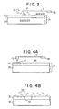
- Fig. 3 illustrates the use of the present invention to provide a fine-line deposition directly on an insulating substrate in a direct-write process.
- This technique has some similarities to that shown in U.S. 4,550,257, but is significantly different in that the substrate does not provide a highly conducting current return path between the pointed tip 10 and the substrate.
- the layer 26 may be an insulator which is not a resist layer.
- a gas, indicated by the wavy lines 46, is located in the vicinity of the pointed tip 10, and is present between the apex of the pointed tip and the insulation surface 26.
- field emission can be used to create electrons which travel to the insulator surface and dissociate or decompose gas molecules located on or near the surface of insulator 26. This causes materials to be deposited from the dissociated gas molecules.
- An example is a gas such as tungsten hexafluoride (WF6) or boron trifluoride (BF3).
- WF6 tungsten hexafluoride
- BF3 boron trifluoride
- Other gases that can be used to deposit metals include trimethyl aluminum Al(CH3)3 and tungsten hexacarbonyl W(CO6). It is also possible to deposit other than metals on the surface of insulator 26 using the present invention.
- a gas such as disilane (Si2H6) can be dissociated to deposit silicon.
- Figs. 4A and 4B illustrate a technique in which the apparatus of Fig. 1 is used to etch very fine regions in the surface of the insulator 26.
- the electrons emitted from pointed tip 10 cause a negative charging of localized regions in the surface of insulator 26, as illustrated by the "minus" marks 48.
- an oppositely charged gas, plasma or particle cloud indicated by wavy lines 50 in Fig. 4B, is brought to the surface of layer 26, the localized charged areas can be etched to produce the fine-line etched regions 52.
- An example of an oppositely charged gas or particle cloud which can be used to etch a negatively charged region in an insulator is (CF3)+.
- the oppositely charged gas or particle cloud can be one which will react with the localized charged regions 48 to cause decomposition or dissociation of the gas or particle cloud to deposit a species only in the area showing the localized charges.
- An example of such a charged gas is (WF5)+).
- the applied voltages can be very small, typically less than 100 volts, and more typically less than about 40 volts. Because the electron beam is so narrow and because only low voltage electrons need be utilized, problems associated with conventional electron apparatus such as a scanning electron microscope (SEM) are avoided. Further, the limitations attendant with a scanning tunneling microscope type of apparatus, as utilized in aforementioned U.S. Patents 4,550,257 and 4,785,189, are avoided since a tunneling current and a highly conducting current return path are not required.
- the pointed tip of this invention can be used to provide high resolution patterns on insulating substrates with resolutions not obtainable by conventional SEM-type apparatus.
- a 5000 V SEM cannot expose a resist layer with a resolution of 10 nm (100 ⁇ ) because the electron beam cannot be focussed to 10 nm (100 ⁇ ) at these voltages.
- a tip voltage of 5000 V can be used to expose a resist layer with 100 nm (100 ⁇ ) resolution.
- the present invention can be used to scan an insulating substrate where the impedance of the entire current path is very high, being about 1010 ohms and larger.
- the current necessary for feedback control having scanning would not be obtainable when the current path has these high impedances.
Landscapes
- Engineering & Computer Science (AREA)
- Chemical & Material Sciences (AREA)
- Physics & Mathematics (AREA)
- General Physics & Mathematics (AREA)
- Nanotechnology (AREA)
- Crystallography & Structural Chemistry (AREA)
- Analytical Chemistry (AREA)
- Mathematical Physics (AREA)
- Theoretical Computer Science (AREA)
- Condensed Matter Physics & Semiconductors (AREA)
- Manufacturing & Machinery (AREA)
- Electron Beam Exposure (AREA)
- Exposure And Positioning Against Photoresist Photosensitive Materials (AREA)
- Drying Of Semiconductors (AREA)
- Physical Deposition Of Substances That Are Components Of Semiconductor Devices (AREA)
- Exposure Of Semiconductors, Excluding Electron Or Ion Beam Exposure (AREA)
Applications Claiming Priority (2)
| Application Number | Priority Date | Filing Date | Title |
|---|---|---|---|
| US594269 | 1984-03-28 | ||
| US07/594,269 US5047649A (en) | 1990-10-09 | 1990-10-09 | Method and apparatus for writing or etching narrow linewidth patterns on insulating materials |
Publications (3)
| Publication Number | Publication Date |
|---|---|
| EP0480183A2 true EP0480183A2 (fr) | 1992-04-15 |
| EP0480183A3 EP0480183A3 (en) | 1992-06-10 |
| EP0480183B1 EP0480183B1 (fr) | 1996-11-20 |
Family
ID=24378225
Family Applications (1)
| Application Number | Title | Priority Date | Filing Date |
|---|---|---|---|
| EP91115240A Expired - Lifetime EP0480183B1 (fr) | 1990-10-09 | 1991-09-10 | Méthode et appareil pour écrire ou graver des motifs de lignes fines sur des matériaux isolants |
Country Status (4)
| Country | Link |
|---|---|
| US (1) | US5047649A (fr) |
| EP (1) | EP0480183B1 (fr) |
| JP (1) | JP2918076B2 (fr) |
| DE (1) | DE69123216T2 (fr) |
Cited By (9)
| Publication number | Priority date | Publication date | Assignee | Title |
|---|---|---|---|---|
| WO2001080292A1 (fr) * | 2000-04-19 | 2001-10-25 | Hitachi, Ltd. | Dispositif et methode destines a l'application de modeles |
| WO2001084238A1 (fr) * | 2000-05-04 | 2001-11-08 | Btg International Limited | Nanostructures |
| WO2002003142A3 (fr) * | 2000-06-30 | 2002-08-08 | Harvard College | Procede et dispositif pour l'impression de microcontacts electriques |
| EP1533803A3 (fr) * | 2003-11-21 | 2006-07-19 | Pioneer Corporation | Tête d'enregistrement/reproduction,son procédé de fabrication, et appareil d'enregistrement et appareil de reproduction |
| US7232771B2 (en) | 2003-11-04 | 2007-06-19 | Regents Of The University Of Minnesota | Method and apparatus for depositing charge and/or nanoparticles |
| US7385901B2 (en) | 2003-06-12 | 2008-06-10 | Yasuo Cho | Data recording/reproducing apparatus and method using needle-shaped member |
| US7590040B2 (en) | 2003-08-25 | 2009-09-15 | Yasuo Cho | Signal detecting method and apparatus and information reproducing apparatus and method |
| US7592269B2 (en) | 2003-11-04 | 2009-09-22 | Regents Of The University Of Minnesota | Method and apparatus for depositing charge and/or nanoparticles |
| US8945673B2 (en) | 2007-01-22 | 2015-02-03 | Regents Of The University Of Minnesota | Nanoparticles with grafted organic molecules |
Families Citing this family (57)
| Publication number | Priority date | Publication date | Assignee | Title |
|---|---|---|---|---|
| JPH02187944A (ja) * | 1989-01-13 | 1990-07-24 | Sharp Corp | 再生装置 |
| EP0522168A1 (fr) * | 1991-01-11 | 1993-01-13 | Hitachi, Ltd. | Appareil et procede d'usinage d'atomes de surface |
| JPH04355914A (ja) * | 1991-02-06 | 1992-12-09 | Olympus Optical Co Ltd | リソグラフィー装置 |
| US5397420A (en) * | 1991-03-03 | 1995-03-14 | Nippondenso Co., Ltd. | Fine structure forming device |
| US5267471A (en) * | 1992-04-30 | 1993-12-07 | Ibm Corporation | Double cantilever sensor for atomic force microscope |
| JPH0696714A (ja) * | 1992-09-14 | 1994-04-08 | Hitachi Ltd | 表面加工装置および記録装置 |
| JP3270165B2 (ja) * | 1993-01-22 | 2002-04-02 | セイコーインスツルメンツ株式会社 | 表面分析及び加工装置 |
| JP3054900B2 (ja) * | 1993-03-10 | 2000-06-19 | セイコーインスツルメンツ株式会社 | 微細加工装置 |
| DE4316855C1 (de) * | 1993-05-19 | 1994-09-15 | Siemens Ag | Mikroelektronische Schaltungsstruktur und Verfahren zu deren Herstellung |
| US5504338A (en) * | 1993-06-30 | 1996-04-02 | The United States Of America As Represented By The Secretary Of The Navy | Apparatus and method using low-voltage and/or low-current scanning probe lithography |
| US5474640A (en) * | 1993-07-19 | 1995-12-12 | Applied Materials, Inc. | Apparatus for marking a substrate using ionized gas |
| US5383354A (en) * | 1993-12-27 | 1995-01-24 | Motorola, Inc. | Process for measuring surface topography using atomic force microscopy |
| US6337479B1 (en) | 1994-07-28 | 2002-01-08 | Victor B. Kley | Object inspection and/or modification system and method |
| US5751683A (en) | 1995-07-24 | 1998-05-12 | General Nanotechnology, L.L.C. | Nanometer scale data storage device and associated positioning system |
| US6353219B1 (en) | 1994-07-28 | 2002-03-05 | Victor B. Kley | Object inspection and/or modification system and method |
| US6339217B1 (en) | 1995-07-28 | 2002-01-15 | General Nanotechnology Llc | Scanning probe microscope assembly and method for making spectrophotometric, near-field, and scanning probe measurements |
| US6507553B2 (en) | 1995-07-24 | 2003-01-14 | General Nanotechnology Llc | Nanometer scale data storage device and associated positioning system |
| US5831181A (en) * | 1995-09-29 | 1998-11-03 | The Regents Of The University Of California | Automated tool for precision machining and imaging |
| US5874668A (en) * | 1995-10-24 | 1999-02-23 | Arch Development Corporation | Atomic force microscope for biological specimens |
| US5874734A (en) * | 1996-12-31 | 1999-02-23 | Elings; Virgil B. | Atomic force microscope for measuring properties of dielectric and insulating layers |
| KR100543054B1 (ko) * | 1997-10-24 | 2006-01-20 | 리처드 제이 푸고 | 무선주파수 전자기장 발생기를 이용한 플라즈마 절개 방법 |
| US6923044B1 (en) | 2001-03-08 | 2005-08-02 | General Nanotechnology Llc | Active cantilever for nanomachining and metrology |
| US6802646B1 (en) | 2001-04-30 | 2004-10-12 | General Nanotechnology Llc | Low-friction moving interfaces in micromachines and nanomachines |
| US6752008B1 (en) | 2001-03-08 | 2004-06-22 | General Nanotechnology Llc | Method and apparatus for scanning in scanning probe microscopy and presenting results |
| US7196328B1 (en) | 2001-03-08 | 2007-03-27 | General Nanotechnology Llc | Nanomachining method and apparatus |
| US6787768B1 (en) | 2001-03-08 | 2004-09-07 | General Nanotechnology Llc | Method and apparatus for tool and tip design for nanomachining and measurement |
| US6251755B1 (en) * | 1999-04-22 | 2001-06-26 | International Business Machines Corporation | High resolution dopant/impurity incorporation in semiconductors via a scanned atomic force probe |
| WO2001003157A1 (fr) | 1999-07-01 | 2001-01-11 | General Nanotechnology, Llc | Systeme et procede servant a inspecter et/ou modifier un objet |
| US6262426B1 (en) | 1999-10-27 | 2001-07-17 | S&F Technological Development And Solutions Partners | Technique and process for the imaging and formation of various devices and surfaces |
| KR100331451B1 (ko) * | 2000-05-10 | 2002-04-09 | 윤종용 | 탄소 함유 물질을 이용한 재기록 가능한 데이타 스토리지및 그 기록/재생 방법 |
| US6730370B1 (en) * | 2000-09-26 | 2004-05-04 | Sveinn Olafsson | Method and apparatus for processing materials by applying a controlled succession of thermal spikes or shockwaves through a growth medium |
| US6931710B2 (en) | 2001-01-30 | 2005-08-23 | General Nanotechnology Llc | Manufacturing of micro-objects such as miniature diamond tool tips |
| US7253407B1 (en) | 2001-03-08 | 2007-08-07 | General Nanotechnology Llc | Active cantilever for nanomachining and metrology |
| US7053369B1 (en) | 2001-10-19 | 2006-05-30 | Rave Llc | Scan data collection for better overall data accuracy |
| US6813937B2 (en) | 2001-11-28 | 2004-11-09 | General Nanotechnology Llc | Method and apparatus for micromachines, microstructures, nanomachines and nanostructures |
| JP4017104B2 (ja) * | 2002-07-09 | 2007-12-05 | パイオニア株式会社 | 誘電体記録再生ヘッド及びトラッキング方法 |
| EP1539637A4 (fr) | 2002-09-09 | 2010-07-28 | Gen Nanotechnology Llc | Delivrance de fluide pour la microscopie balayage par sonde |
| US20060151435A1 (en) * | 2002-09-18 | 2006-07-13 | Jun Taniguchi | Surface processing method |
| US20070014047A1 (en) * | 2003-05-01 | 2007-01-18 | Yasuo Cho | Recording/reproduction head and recording/reproduction device |
| CN100379688C (zh) * | 2003-08-22 | 2008-04-09 | Fmc福瑞特股份有限公司 | 用于废水净化的方法、装置和试剂 |
| US7550747B2 (en) * | 2006-04-03 | 2009-06-23 | Blaise Laurent Mouttet | Parallel electron beam lithography stamp (PEBLS) |
| US7425715B2 (en) * | 2006-05-05 | 2008-09-16 | Blaise Laurent Mouttet | Digital parallel electron beam lithography stamp |
| US7807062B2 (en) * | 2006-07-10 | 2010-10-05 | Micron Technology, Inc. | Electron induced chemical etching and deposition for local circuit repair |
| US7791055B2 (en) | 2006-07-10 | 2010-09-07 | Micron Technology, Inc. | Electron induced chemical etching/deposition for enhanced detection of surface defects |
| US7892978B2 (en) * | 2006-07-10 | 2011-02-22 | Micron Technology, Inc. | Electron induced chemical etching for device level diagnosis |
| US7791071B2 (en) | 2006-08-14 | 2010-09-07 | Micron Technology, Inc. | Profiling solid state samples |
| US7833427B2 (en) | 2006-08-14 | 2010-11-16 | Micron Technology, Inc. | Electron beam etching device and method |
| US7718080B2 (en) * | 2006-08-14 | 2010-05-18 | Micron Technology, Inc. | Electronic beam processing device and method using carbon nanotube emitter |
| WO2008021321A2 (fr) * | 2006-08-17 | 2008-02-21 | Rjf Holdings Iv, Inc | procédé et appareil pour l'incision d'un tissu CARDIOVASCULAIRE par plasma |
| JP4309438B2 (ja) * | 2007-03-20 | 2009-08-05 | 株式会社東芝 | 情報記録再生装置 |
| EP1975592A1 (fr) * | 2007-03-28 | 2008-10-01 | F. Hoffmann-la Roche AG | Micro-réseau de sorption |
| US10330581B2 (en) | 2007-09-17 | 2019-06-25 | Rave Llc | Debris removal from high aspect structures |
| US10384238B2 (en) | 2007-09-17 | 2019-08-20 | Rave Llc | Debris removal in high aspect structures |
| US10618080B2 (en) * | 2007-09-17 | 2020-04-14 | Bruker Nano, Inc. | Debris removal from high aspect structures |
| US8689358B2 (en) * | 2010-06-28 | 2014-04-01 | International Business Machines Corporation | Dynamic mode nano-scale imaging and position control using deflection signal direct sampling of higher mode-actuated microcantilevers |
| EP2834709B1 (fr) * | 2012-04-02 | 2020-05-27 | ASML Netherlands B.V. | Procédé et appareil de mesure de contamination de matière particulaire |
| DE102018206278B4 (de) | 2018-04-24 | 2026-02-19 | Carl Zeiss Smt Gmbh | Verfahren und Vorrichtung zum Entfernen eines Partikels von einer photolithographischen Maske |
Family Cites Families (14)
| Publication number | Priority date | Publication date | Assignee | Title |
|---|---|---|---|---|
| JPS6031905B2 (ja) * | 1977-02-22 | 1985-07-25 | 超エル・エス・アイ技術研究組合 | 部分イオンエッチング法 |
| US4316093A (en) * | 1979-02-12 | 1982-02-16 | International Business Machines Corporation | Sub-100A range line width pattern fabrication |
| CH643397A5 (de) * | 1979-09-20 | 1984-05-30 | Ibm | Raster-tunnelmikroskop. |
| EP0071666B1 (fr) * | 1981-08-10 | 1985-02-06 | International Business Machines Corporation | Support mobile électrique |
| US4550257A (en) * | 1984-06-29 | 1985-10-29 | International Business Machines Corporation | Narrow line width pattern fabrication |
| US4907195A (en) * | 1984-09-14 | 1990-03-06 | Xerox Corporation | Method of and system for atomic scale recording of information |
| DE3570012D1 (en) * | 1985-01-29 | 1989-06-08 | Ibm | Field-emission scanning auger electron microscope |
| DE3572030D1 (en) * | 1985-03-07 | 1989-09-07 | Ibm | Scanning tunneling microscope |
| JPH0712013B2 (ja) * | 1985-04-29 | 1995-02-08 | インタ−ナショナル ビジネス マシ−ンズ コ−ポレ−ション | 低エネルギ電子ビーム・リソグラフイ露光装置及びその方法 |
| US4785189A (en) * | 1985-04-29 | 1988-11-15 | International Business Machines Corporation | Method and apparatus for low-energy scanning electron beam lithography |
| US4724318A (en) * | 1985-11-26 | 1988-02-09 | International Business Machines Corporation | Atomic force microscope and method for imaging surfaces with atomic resolution |
| US4823004A (en) * | 1987-11-24 | 1989-04-18 | California Institute Of Technology | Tunnel and field effect carrier ballistics |
| JPH02173278A (ja) * | 1988-12-26 | 1990-07-04 | Hitachi Ltd | 微細加工方法及びその装置 |
| JPH02295050A (ja) * | 1989-05-09 | 1990-12-05 | Olympus Optical Co Ltd | μ―STMを用いた回路パターン作製装置および回路パターン作製方法 |
-
1990
- 1990-10-09 US US07/594,269 patent/US5047649A/en not_active Expired - Lifetime
-
1991
- 1991-07-30 JP JP3212656A patent/JP2918076B2/ja not_active Expired - Fee Related
- 1991-09-10 DE DE69123216T patent/DE69123216T2/de not_active Expired - Fee Related
- 1991-09-10 EP EP91115240A patent/EP0480183B1/fr not_active Expired - Lifetime
Cited By (15)
| Publication number | Priority date | Publication date | Assignee | Title |
|---|---|---|---|---|
| WO2001080292A1 (fr) * | 2000-04-19 | 2001-10-25 | Hitachi, Ltd. | Dispositif et methode destines a l'application de modeles |
| KR100756211B1 (ko) * | 2000-05-04 | 2007-09-06 | 비티지 인터내셔널 리미티드 | 나노구조물 |
| WO2001084238A1 (fr) * | 2000-05-04 | 2001-11-08 | Btg International Limited | Nanostructures |
| AU784574B2 (en) * | 2000-05-04 | 2006-05-04 | Qunano Ab | Nanostructures |
| US7223444B2 (en) | 2000-05-04 | 2007-05-29 | Qunano Ab | Particle deposition apparatus and methods for forming nanostructures |
| CN100335968C (zh) * | 2000-05-04 | 2007-09-05 | 英国技术集团国际有限公司 | 纳米结构 |
| WO2002003142A3 (fr) * | 2000-06-30 | 2002-08-08 | Harvard College | Procede et dispositif pour l'impression de microcontacts electriques |
| US7771647B2 (en) | 2000-06-30 | 2010-08-10 | President And Fellows Of Harvard College | Electric microcontact printing method and apparatus |
| US7385901B2 (en) | 2003-06-12 | 2008-06-10 | Yasuo Cho | Data recording/reproducing apparatus and method using needle-shaped member |
| US8004948B2 (en) | 2003-06-12 | 2011-08-23 | Yasuo Cho | Data recording / reproducing apparatus and method using needle-shaped member |
| US7590040B2 (en) | 2003-08-25 | 2009-09-15 | Yasuo Cho | Signal detecting method and apparatus and information reproducing apparatus and method |
| US7232771B2 (en) | 2003-11-04 | 2007-06-19 | Regents Of The University Of Minnesota | Method and apparatus for depositing charge and/or nanoparticles |
| US7592269B2 (en) | 2003-11-04 | 2009-09-22 | Regents Of The University Of Minnesota | Method and apparatus for depositing charge and/or nanoparticles |
| EP1533803A3 (fr) * | 2003-11-21 | 2006-07-19 | Pioneer Corporation | Tête d'enregistrement/reproduction,son procédé de fabrication, et appareil d'enregistrement et appareil de reproduction |
| US8945673B2 (en) | 2007-01-22 | 2015-02-03 | Regents Of The University Of Minnesota | Nanoparticles with grafted organic molecules |
Also Published As
| Publication number | Publication date |
|---|---|
| JP2918076B2 (ja) | 1999-07-12 |
| DE69123216D1 (de) | 1997-01-02 |
| US5047649A (en) | 1991-09-10 |
| JPH04288815A (ja) | 1992-10-13 |
| EP0480183A3 (en) | 1992-06-10 |
| EP0480183B1 (fr) | 1996-11-20 |
| DE69123216T2 (de) | 1997-04-30 |
Similar Documents
| Publication | Publication Date | Title |
|---|---|---|
| EP0480183B1 (fr) | Méthode et appareil pour écrire ou graver des motifs de lignes fines sur des matériaux isolants | |
| US6087274A (en) | Nanoscale X-Y-Z translation of nanochannel glass replica-based masks for making complex structures during patterning | |
| US9070556B2 (en) | Patterning of nanostructures | |
| US6007969A (en) | Ultra-fine microfabrication method using an energy beam | |
| US4785189A (en) | Method and apparatus for low-energy scanning electron beam lithography | |
| EP0166119B1 (fr) | Procédé pour le dépôt de matériau dans les dimensions du nanomètre | |
| US5478698A (en) | Direct-write afocal electron-beam semiconductor lithography | |
| Ochiai et al. | Ten-nanometer resolution nanolithography using newly developed 50-kv electron beam direct writing system | |
| US6777693B2 (en) | Lithographic method using ultra-fine probe needle | |
| US5504338A (en) | Apparatus and method using low-voltage and/or low-current scanning probe lithography | |
| US7579050B2 (en) | Method for focusing patterning nano-sized structure | |
| US5171718A (en) | Method for forming a fine pattern by using a patterned resist layer | |
| US20040060904A1 (en) | Tool having a plurality of electrodes and corresponding method of altering a very small surface | |
| EP0200083B1 (fr) | Appareil de lithographie par balayage d'un faisceau électronique de basse énergie | |
| Ishibashi et al. | Characteristics of nanoscale lithography using AFM with a current-controlled exposure system | |
| JP3022948B2 (ja) | 超微細加工法 | |
| JPS6317246Y2 (fr) | ||
| EP0268595B1 (fr) | Procede de transfert de configurations pour fabriquer des dispositifs a circuits integres | |
| KR100792385B1 (ko) | 나노팁전자방출원, 그의 제조 방법 및 그를 구비한 나노팁리소그래피 장치 | |
| EP0318037A2 (fr) | Méthode pour l'obtention de textures très fines en utilisant une couche texturée résistante | |
| Chang et al. | Arrayed lithography using STM-based microcolumns | |
| McCord et al. | Principles and techniques of STM lithography | |
| JPH04258109A (ja) | X線露光装置及びx線露光方法 | |
| Soh et al. | Resist exposure using field-emitted electrons | |
| Marrian et al. | Reduction and Elimination of Proximity Effects |
Legal Events
| Date | Code | Title | Description |
|---|---|---|---|
| PUAI | Public reference made under article 153(3) epc to a published international application that has entered the european phase |
Free format text: ORIGINAL CODE: 0009012 |
|
| AK | Designated contracting states |
Kind code of ref document: A2 Designated state(s): DE FR GB IT |
|
| PUAL | Search report despatched |
Free format text: ORIGINAL CODE: 0009013 |
|
| AK | Designated contracting states |
Kind code of ref document: A3 Designated state(s): DE FR GB IT |
|
| 17P | Request for examination filed |
Effective date: 19920817 |
|
| 17Q | First examination report despatched |
Effective date: 19941114 |
|
| GRAG | Despatch of communication of intention to grant |
Free format text: ORIGINAL CODE: EPIDOS AGRA |
|
| GRAH | Despatch of communication of intention to grant a patent |
Free format text: ORIGINAL CODE: EPIDOS IGRA |
|
| GRAH | Despatch of communication of intention to grant a patent |
Free format text: ORIGINAL CODE: EPIDOS IGRA |
|
| GRAA | (expected) grant |
Free format text: ORIGINAL CODE: 0009210 |
|
| AK | Designated contracting states |
Kind code of ref document: B1 Designated state(s): DE FR GB IT |
|
| PG25 | Lapsed in a contracting state [announced via postgrant information from national office to epo] |
Ref country code: IT Free format text: LAPSE BECAUSE OF FAILURE TO SUBMIT A TRANSLATION OF THE DESCRIPTION OR TO PAY THE FEE WITHIN THE PRE;WARNING: LAPSES OF ITALIAN PATENTS WITH EFFECTIVE DATE BEFORE 2007 MAY HAVE OCCURRED AT ANY TIME BEFORE 2007. THE CORRECT EFFECTIVE DATE MAY BE DIFFERENT FROM THE ONE RECORDED.SCRIBED TIME-LIMIT Effective date: 19961120 Ref country code: FR Effective date: 19961120 |
|
| REF | Corresponds to: |
Ref document number: 69123216 Country of ref document: DE Date of ref document: 19970102 |
|
| EN | Fr: translation not filed | ||
| PG25 | Lapsed in a contracting state [announced via postgrant information from national office to epo] |
Ref country code: GB Free format text: LAPSE BECAUSE OF NON-PAYMENT OF DUE FEES Effective date: 19970910 |
|
| PLBE | No opposition filed within time limit |
Free format text: ORIGINAL CODE: 0009261 |
|
| STAA | Information on the status of an ep patent application or granted ep patent |
Free format text: STATUS: NO OPPOSITION FILED WITHIN TIME LIMIT |
|
| 26N | No opposition filed | ||
| GBPC | Gb: european patent ceased through non-payment of renewal fee |
Effective date: 19970910 |
|
| PGFP | Annual fee paid to national office [announced via postgrant information from national office to epo] |
Ref country code: DE Payment date: 19990916 Year of fee payment: 9 |
|
| PG25 | Lapsed in a contracting state [announced via postgrant information from national office to epo] |
Ref country code: DE Free format text: LAPSE BECAUSE OF NON-PAYMENT OF DUE FEES Effective date: 20010601 |