EP0480421A2 - Architecture de RAM testable dans un microprocesseur ayant une antémémoire encastrée - Google Patents
Architecture de RAM testable dans un microprocesseur ayant une antémémoire encastrée Download PDFInfo
- Publication number
- EP0480421A2 EP0480421A2 EP91117293A EP91117293A EP0480421A2 EP 0480421 A2 EP0480421 A2 EP 0480421A2 EP 91117293 A EP91117293 A EP 91117293A EP 91117293 A EP91117293 A EP 91117293A EP 0480421 A2 EP0480421 A2 EP 0480421A2
- Authority
- EP
- European Patent Office
- Prior art keywords
- cache
- data
- cpu
- instruction
- tag
- Prior art date
- Legal status (The legal status is an assumption and is not a legal conclusion. Google has not performed a legal analysis and makes no representation as to the accuracy of the status listed.)
- Granted
Links
Images





Classifications
-
- G—PHYSICS
- G11—INFORMATION STORAGE
- G11C—STATIC STORES
- G11C11/00—Digital stores characterised by the use of particular electric or magnetic storage elements; Storage elements therefor
- G11C11/21—Digital stores characterised by the use of particular electric or magnetic storage elements; Storage elements therefor using electric elements
- G11C11/34—Digital stores characterised by the use of particular electric or magnetic storage elements; Storage elements therefor using electric elements using semiconductor devices
- G11C11/40—Digital stores characterised by the use of particular electric or magnetic storage elements; Storage elements therefor using electric elements using semiconductor devices using transistors
-
- G—PHYSICS
- G06—COMPUTING OR CALCULATING; COUNTING
- G06F—ELECTRIC DIGITAL DATA PROCESSING
- G06F11/00—Error detection; Error correction; Monitoring
- G06F11/22—Detection or location of defective computer hardware by testing during standby operation or during idle time, e.g. start-up testing
- G06F11/2205—Detection or location of defective computer hardware by testing during standby operation or during idle time, e.g. start-up testing using arrangements specific to the hardware being tested
- G06F11/2236—Detection or location of defective computer hardware by testing during standby operation or during idle time, e.g. start-up testing using arrangements specific to the hardware being tested to test CPU or processors
-
- G—PHYSICS
- G06—COMPUTING OR CALCULATING; COUNTING
- G06F—ELECTRIC DIGITAL DATA PROCESSING
- G06F11/00—Error detection; Error correction; Monitoring
- G06F11/22—Detection or location of defective computer hardware by testing during standby operation or during idle time, e.g. start-up testing
- G06F11/26—Functional testing
- G06F11/273—Tester hardware, i.e. output processing circuits
- G06F11/2733—Test interface between tester and unit under test
-
- G—PHYSICS
- G06—COMPUTING OR CALCULATING; COUNTING
- G06F—ELECTRIC DIGITAL DATA PROCESSING
- G06F12/00—Accessing, addressing or allocating within memory systems or architectures
- G06F12/02—Addressing or allocation; Relocation
- G06F12/08—Addressing or allocation; Relocation in hierarchically structured memory systems, e.g. virtual memory systems
- G06F12/0802—Addressing of a memory level in which the access to the desired data or data block requires associative addressing means, e.g. caches
-
- G—PHYSICS
- G11—INFORMATION STORAGE
- G11C—STATIC STORES
- G11C29/00—Checking stores for correct operation ; Subsequent repair; Testing stores during standby or offline operation
- G11C29/04—Detection or location of defective memory elements, e.g. cell constructio details, timing of test signals
- G11C29/08—Functional testing, e.g. testing during refresh, power-on self testing [POST] or distributed testing
- G11C29/12—Built-in arrangements for testing, e.g. built-in self testing [BIST] or interconnection details
- G11C29/18—Address generation devices; Devices for accessing memories, e.g. details of addressing circuits
- G11C29/24—Accessing extra cells, e.g. dummy cells or redundant cells
-
- G—PHYSICS
- G11—INFORMATION STORAGE
- G11C—STATIC STORES
- G11C29/00—Checking stores for correct operation ; Subsequent repair; Testing stores during standby or offline operation
- G11C29/04—Detection or location of defective memory elements, e.g. cell constructio details, timing of test signals
- G11C29/08—Functional testing, e.g. testing during refresh, power-on self testing [POST] or distributed testing
- G11C29/12—Built-in arrangements for testing, e.g. built-in self testing [BIST] or interconnection details
- G11C29/36—Data generation devices, e.g. data inverters
-
- G—PHYSICS
- G11—INFORMATION STORAGE
- G11C—STATIC STORES
- G11C29/00—Checking stores for correct operation ; Subsequent repair; Testing stores during standby or offline operation
- G11C29/04—Detection or location of defective memory elements, e.g. cell constructio details, timing of test signals
- G11C29/08—Functional testing, e.g. testing during refresh, power-on self testing [POST] or distributed testing
- G11C29/48—Arrangements in static stores specially adapted for testing by means external to the store, e.g. using direct memory access [DMA] or using auxiliary access paths
-
- G—PHYSICS
- G01—MEASURING; TESTING
- G01R—MEASURING ELECTRIC VARIABLES; MEASURING MAGNETIC VARIABLES
- G01R31/00—Arrangements for testing electric properties; Arrangements for locating electric faults; Arrangements for electrical testing characterised by what is being tested not provided for elsewhere
- G01R31/28—Testing of electronic circuits, e.g. by signal tracer
- G01R31/317—Testing of digital circuits
- G01R31/3181—Functional testing
- G01R31/319—Tester hardware, i.e. output processing circuits
- G01R31/31903—Tester hardware, i.e. output processing circuits tester configuration
- G01R31/31905—Interface with the device under test [DUT], e.g. arrangements between the test head and the DUT, mechanical aspects, fixture
Definitions
- the present invention relates to microprocessors and, more particularly, to those having on-chip (embedded) cache memory.
- cache memory is SRAM-based (Static Random Access Memory), having access times on the order of 20 nanoseconds (ns), and the main memory is DRAM-based (Dynamic Random Access Memory), having access times on the order of 80-150 ns. While SRAM is generally faster, it is generally more expensive than DRAM. However, the cost/performance tradeoff can be minimized by using a relatively small cache (e.g., 32 Kbytes) to provide quick access to blocks of a relatively large main memory.
- Various algorithms are known and employed to manage cache operation, but the present invention is not limited by the choice of algorithm.
- U.S. Patent No. 4,945,512 issued July 31, 1990, discloses a high speed associative cache memory wherein each of four data array boards comprise a quarter word data array, a full tag array and a memory address register. Each (quarter word) data array board also includes a match comparator for comparing the tag portion of the memory address to the output of the tag array, and generates four tag compare signals which are applied to monitoring and error detection circuits.
- U.S. Patent No. 4,945,472 issued July 31, 1990, discloses a data processor with I/O area detection, and is illustrative of a data processing system having a data processor, memory, and I/O interface, all of which are interconnected via an address bus, a data bus and a control bus.
- U.S. Patent No. 4,937,781 discloses a dual port ram with arbitration status register, and is illustrative of a multi-port RAM having an array of memory locations for storing data, with each of the memory locations having an address associated therewith.
- Figure 1 shows a typical cache architecture 100.
- Main memory (not shown) is accessed by a microprocessor (not shown) over an address bus 102 and a data bus 104.
- the address bus 102 is 32 bits wide (A31..A0), for accessing up to a gigabyte of main memory
- the data bus is 32 bits wide (D31..D0).
- Cache memory 106 is divided into two portions (parts) - a "data" part 108 and a "tag" part 110.
- the size of the data part 108 is 32Kx32 (for storing 32K 32-bit words).
- the 32Kx32 data part 108 may be formed as a 128Kx8 SRAM array.
- a low order portion (A16..A2) of the (main memory) address is provided to the data part 108. This may involve stripping the low order portion of the address off a full 32-bit data bus, or by providing separate low order (AdrLo) and high order (AdrHi) portions of the address bus.
- the low order portion (A16..A2) of the address corresponds on a one-to-one basis with the 32K physical locations (P14..P0) in the data part 108, and is used to select one of those locations, or "cells", for example location "AF73-data" (hex), for storing a data word.
- the first two bits A0,A1 of the address may be used for byte gathering, i.e. for assembling four 8-bit bytes into a 32 bit word.
- the 32-bit data word (D0..D31) corresponding to the full address is provided over the data bus 104 to the selected location ("AF73-data") in the data part 108.
- the tag part 110 has 32K physical locations (T14..T0).
- the higher order portion (A31..A17) of the address (A0..A30) is provided to the tag part 110 in a location corresponding on a one-to-one basis to the selected location (AF73-data) of the stored data in the data part 108.
- the higher order portion of the address (A31..A17) would be stored in location "AF73-tag" in the tag part 110.
- the tag part 110 can be smaller than the data part 108.
- the tag part is 32Kx14.
- Data stored in cache memory can be either "data” or "instructions".
- cache memory is segmented into a “data” cache (DCache) having a data part and a tag part, and an “instruction” cache (ICache) having a data part (containing “instructions") and a tag part.
- DCache data cache
- ICache instruction cache
- the data cache and instruction cache operate identically, although they may be sized differently.
- discussion directed to data cache is applicable to instruction cache.
- testing the data (or instruction) part is relatively straightforward.
- the contents of selected locations of the data part 112 are read, or tested (by the microprocessor, not shown) against what was written thereto.
- Testing the tag part is somewhat more involved.
- a read operation is initiated, such as by providing an address over the address bus 102.
- the stored tag (T14..T0) is compared in a comparator 112 with the higher order portion of the address (A31..A17), taken directly from the bus. If they compare, a "hit” signal issues from the comparator. If they mis-match, a "miss” signal issues.
- testable cache memory and, more broadly speaking, a testable RAM architecture in a microprocessor-based system, particularly in a system where the cache is embedded, or on-chip with the microprocessor.
- a microprocessor chip includes a central processing unit (CPU), cache control, cache memory and a bus interface unit (BIU).
- CPU central processing unit
- BIU bus interface unit
- a special test mode of operation is provided for the cache controller and the bus interface unit. The test mode is initiated by an external tester which then directly accesses the cache to read or write the data (or instruction) and tag parts thereof. Once access is made, the tester can verify the integrity of the individual RAMs by writing and reading patterns.
- test mode of operation is entered when the BIU grants a "Test Mode Read” or “Test Mode Write” request for either the instruction or the data cache.
- Test mode requests There are 4 types of "test” mode requests: 1) Instruction Cache Test Mode Read; 2) Instruction Cache Test Mode Write; 3) Data cache Test Mode Read; and 4) Data Cache Test Mode Write.
- the tester provides an address to the BIU of the cache location to be tested.
- the BIU passes this address to the cache controller which uses it to access the proper location in the tag part.
- the tester also provides the BIU with a "bit pattern" to be written.
- the BIU passes this bit pattern to the cache controller which will write it at the addressed location. If it is a "Test Mode Read” request, the cache controller will provide the BIU with the bit pattern stored at the addressed location along with a cache "Hit/Miss" signal. The BIU passes this bit pattern and the "Hit/Miss” signal to the tester.
- the cache comparator itself can be tested for proper operation by "forcing" misses at specific locations in cache, and checking for appropriate comparator output. In other words, if one bit pattern is written to a cache location, and a different bit pattern is provided with a read request, the comparator should issue a "miss" signal.
- central processing unit or processor
- RAM Random Access Memory
- DRAM Dynamic RAM
- SRAM Static RAM
- I/O Input/Output
- kilo k
- signals are designated by generally accepted acronyms, such as enable (EN), read (RD), write (WR), fetch (FTCH), memory (M), data (D), instruction (I), test (TEST), acknowledge (ACK), block (BLK), etc., which may be compounded to provide descriptive signal names.
- these signals are followed by a notation [##:#] or (B##..B#) which indicates byte-wide signals, and their bit count.
- Figure 1 is a block diagram of a typical cache memory.
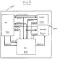
- FIG. 2 is a block diagram of a microprocessor with embedded cache memory, according to the present invention.
- Figure 3 is a block diagram of an exemplary configuration for the cache memory of Figure 2.
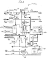
- FIG. 4 is a functional block diagram of the Bus Interface Unit (BIU) of Figure 2.
- BIU Bus Interface Unit
- Figure 5A is a block diagram of the interface between the instruction cache and the BIU of Figure 2.
- Figure 5B is a block diagram of the interface between the data cache and BIU of Figure 2.
- Figure 5C is a block diagram of the interface between the instruction and data caches and the CPU of Figure 2.
- Figure 5D is a block diagram of the interface between the CPU, the BIU, the cache, and an external tester, according to the present invention.
- Figure 1 describes organization and function of a typical cache memory, and is described hereinabove.
- FIG. 2 shows the general (gross) architecture of an embedded cache memory microprocessor 200, according to the present invention, which includes a central processing unit (CPU) 202, a cache 204, and a bus interface unit (BIU) 206.
- the cache 204 is partitioned into an Instruction Cache (ICache) 204i and a Data Cache (DCache) 204d, each of which has corresponding instruction or data parts and tag parts.
- the present invention is primarily concerned with testing (exercising) the embedded tag part or parts, whether or not cache is partitioned into ICache or DCache,
- An LR3000 Microprocessor available from LSI Logic Corporation, Milpitas, CA, is suitably employed for the CPU 102.
- the LR3000 Microprocessor is a MIPS (trademark of MIPS Computer Systems Inc.) RISC (Reduced Instruction Set Computer) microprocessor, and includes on-chip memory management, cache interface and control and main memory control logic.
- the LR3000's on-chip memory management function is fully associative, employing a 64-entry translation lookaside buffer.
- the on-chip cache control manages separate external instruction and data caches, of up to 356 Kbytes each, both of which can be accessed during a single CPU cycle.
- the LR3000 generates all the required cache and main memory control and address signals for attached coprocessors
- the existing LR3000's on-chip cache control supports external instruction and data cache memories, up to 256 Kbytes (from 4 Kbytes to 256 Kbytes) each, and both cache memories can be accessed during a single CPU cycle.
- the caches are direct-mapped, and "normally" (without the improvements of the present invention) would be built using commercially available, high speed SRAMs.
- the LR3000 processor directly drives the cache control signals, eliminating the skew and delay of external buffers.
- the LR3000 supports block refill of both the instruction and data caches.
- the D-Cache can be isolated from main memory, and the instruction and data caches can be swapped. These operations are used to support cache flushing, diagnostics and trouble-shooting.
- the instruction and data caches are preferably embedded (on-chip) with the CPU. (There are easier ways to test external caches than the techniques disclosed herein )
- the "normal" (external) signal configuration of the LR3000 Microprocessor includes:
- an additional external signal from the cache comparator output indicates a cache hit or miss during cache reads and writes.
- FIG. 3 shows the gross physical organization of the cache 204.
- Cache 204 includes instruction data part (ID) 302, an instruction tag part (ITag) 304, a data data part (DD) 306 and a data tag part (DTag) 308.
- ITag instruction data part
- DD data data part
- DTag data tag part
- These parts 302, 304, 306 and 308 are made up of SRAM arrays, configured as noted in the drawing (e.g., the ID part 302 is a 1Kx32 SRAM array).
- the ID part 302 holds 1K 32-bit instruction words (1Kx32).
- the ITAG part 304 holds 20 bit tag and 4 valid bits for each line (256x24). Both the ID and ITAG parts are preferably high-density RAM arrays with bit read, bit write, tristate outputs and chip select (CS) power down features.
- the DD part 306 holds 256 32-bit data words (256x32).
- the DTag part 308 holds 64 22-bit tag and 4 valid bits for each line (64x26).
- Both the DD and DTAG parts are preferably high-density RAM arrays with bit read, bit write, tristate outputs and CS power down features.
- the Bus Interface Unit (BIU) 206 is the intermediary logic between the CPU 202, the cache 204, and other system components such as timers, DRAM control, etc. It controls the CPU interface to external memory, as well as to on-chip instruction and data caches (ICache and DCache).
- BIU Bus Interface Unit
- FIG. 4 shows functional layout of the BIU 206, which includes the nineteen functional blocks shown. The functions of these blocks are described in detail in Appendix 6. In this section, the blocks are described only briefly, or in greater detail as they are relevant to the present invention, particularly for entering a test mode for direct cache read/writes.
- An Instruction Address Switch (IASWTCH) block 401 determines whether an instruction fetch on a bus (CIA) 420 from the CPU 202 ( Figure 2) is for cacheable or non-cacheable memory space. For cacheable memory space, the IASWTCH issues an ICache select signal on a line 422 to the MBQUEUE (403, discussed below), and waits for a hit/miss indication from the ICache (i.e., the ICache tag comparator), provided over a line 424. Normally, if the ICache indicates a hit, the IASWTCH will issue a request, via the MBQUEUE to the MXCNTL (404, discussed below) to fetch from external memory. This function is bypassed in the test mode of the present invention. Latched addresses are provided to the ICache Address Bus 426, as well as to the BIU's common address bus 426 via transceivers (BABTXVR, discussed below) for presentation off-chip.
- BABTXVR transceivers
- the IASWTCH issues an instruction stall request over a line 430 to the CPU 202 a) during a transaction (reads/writes to cache), b) if an instruction fetch is required, c) when bus snooping is being performed, and d) in the test mode (ICache access mode) of the present invention.
- a Data Address Switch (DASWTCH) block 402 is analogous to the IASWTCH, except that it performs services for the DCache and data memory transactions.
- Latched addresses are provided to the DCAche Address Bus 432, and to the BIU's common address bus 428, and a stall request is issued to the CPU in the test mode.
- a Memory Block Queue (MBQUEUE) block 403 maintains information pertaining to external memory access, including a) an external memory start bit, which is bypassed in the test mode, b) an instruction/data transaction bit for selecting ICache or DCache, c) a cacheable/non-cacheable transaction bit, which is set to "cacheable" in the test mode, and d) a read/write transaction bit, which is provided via MXCNTL (404, discussed below) to the respective instruction and data caches.
- MXCNTL 404, discussed below
- a memory transaction control (MXCNTL) block 404 issues external memory control signals and responds to external control inputs.
- the MXCNTL block issues memory control sequences to the CPU based upon information in the queue of the MBQUEUE block 403.
- Control signals are issued to the appropriate cache over lines 434 (CACHE CONTROL) to perform cache reads/writes, and transaction done signals (TDONE) are issued (to blocks 401, 402, 403, 416 and 417) in response to data ready signals (from lines 436c; DRAM control) from the respective caches.
- An external memory switch control (XMSWTCHCNTL) 405 controls the BIU data path configuration during various operations, which includes test mode read/writes of the instruction and data caches, by issuing a number of data path control signals BC1-BC12. These control signals are described in Appendix 6 (BIU MODULE BLOCK DESCRIPTIONS) at pages 6-7 thereof.
- a data latch (DATLATCH) block 406 is used to sample data on the external memory data bus 436, passing it through to or from a common data bus 438.
- DATLATCH data latch
- an external tester applies data and instructions to the data bus 438 through the DATLATCH 406.
- the tester connects to buses 436a and 436d.
- a block parity (BPAR) block 407 checks parity on read operations. Data (i.e., instructions and data) is provided to this block via the DATLATCH 406 from the external memory data bus 436.
- a byte counter (BYTECTR) block 408 is used to generate the byte address in an 8-bit port fetch where byte gathering is done. (This is more relevant to the aforementioned copending EP-Application No. (Attorney Docket No. LS21087EP ).
- a block address multiplexer (BAMUX) block 409 multiplexes the proper number of bits onto the external memory address bus 436 so that a block address is generated for DRAM or other accesses. (This is more relevant to the aforementioned copending EP-Application No. (Attorney Docket No.LS21087EP ).
- An address latch (ADRLATCH) block 410 requests, in the test mode, appropriate stall cycles for the test mode to be generated in the IASWTCH and DASWTCH blocks (which generate appropriate instruction/data stall requests, as discussed hereinabove).
- An interrupt (INTERRUPT) block 411 latches external interrupt signals on a line 440 and passes them on to the CPU 202 over a line 442.
- a reset (RESET) block 412 (“BRST” in Appendix 6) generates reset signals on a line 444 for cold and warm resets of various elements of the BIU, as well as for the CPU.
- a block transceiver latch (BLTXVRL) 413 connects a latched version of the BIU's common data bus 438 to the CPU's (32-bit) instruction bus (CIBP) 446, via 3-state transceivers. This block provides a flow through path for data during the test mode to/from the ICache and the BIU's common data bus 438.
- a bus transceiver latch (BXXTXVR) 414 connects the CPU's data bus (CDATAP) 448 to a latched version of the BIU's common data bus 438 via 3-state transceivers.
- CDATAP CPU's data bus
- An address bus transceiver (BABTXVR, U11) 415a connects the instruction cache's address bus 426 to the BIU's common address bus 428 via 3-state transceivers. In the test mode, an address supplied by the tester is provided through ADRLATCH 410 over the common address bus 428 to the transceiver 415a.
- a second address bus transceiver (BABTXVR, U9) 415b connects the data cache's address bus 432 to the BIU's common address bus 428 via 3-state transceivers.
- an address supplied by the tester is provided through ADRLATCH 410 over the common address bus 428 to the transceiver 415b.
- a bus address write buffer (BAWBUF) 416 forms an address portion of the write buffer function. In this block, addresses for write transactions are stored until used by an external write transaction.
- a bus data write buffer (BDWBUF) 417 forms a data portion of the write buffer function. In this block, data for write transactions are stored until used by an external write transaction.
- a cache invalidation (BXCINV) block 418 contains a multiplexer which is used to place an invalidation address on the ICache address bus 426.
- Figures 5A-5D show the signal interfaces between the instruction and data caches 204i and 204d, respectively, the BIU 206, the CPU 202 and an external tester 502. These interfaces are discussed in greater detail in Appendix 2 (Module Definition of the Cache Megacell), and at pages 41-59 of Appendix 3 (BIU Module Definition).
- Modes The instruction and data caches are accessed to read or write under four different circumstances, termed “Modes".
- the four different Modes are: “Mode 1”, in which, during a normal run cycle, instructions are read and data is read or written; “Mode 2”, in which, during a block refill, a block of data is written into either the ICache or DCache; “Mode 3”, in which, during testing of the respective cache RAMs, reading and writing to the RAMs takes place; and “Mode 4", in which, during bus snooping on DMA writes, reading and writing to the RAMs may occur.
- the mechanics of accessing the cache are different for each mode, because the source of addresses and the source/destination of data is different in each mode. Also, depending on the mode, the access to cache is either read only or write only or both read and write.
- Mode 1 the CPU issues the addresses and is the source/destination of the data. In this mode, the ICache is read only, whereas the DCache can be read or written.
- the source of address is the address latch/counter in the cache unit, and the source of data is the BIU, which receives the data from main memory.
- the caches are written only - there is no cache read operation.
- the source of address as well as the source/destination of the data is the BIU, which receives the address/data from an external tester (502, Figure 5D). In this mode, the caches can be written and read. "Mode 3" is described in greater detail hereinbelow.
- the source of addresses is the BIU, which receives the addresses from an external bus master such as an external processor, DMA or the like. There is no data transfer in this mode. There is only tag comparison and invalidation.
- FIGS. 6A and 6B show a physical embodiment of the cache 204, which is presented herein only as an example of a viable architecture. The present invention extends beyond testing a particular cache architecture to testing any embedded cache memory while bypassing external memory functions normally implemented during cache reads/writes.
- the cache 204 includes an instruction data part 302, an instruction tag part 304, a data data part 306 and a data tag part 308, which were discussed with respect to Figure 3.
- a cache control 602 is shown, the function of which has already been discussed with respect to Figure 4 as being distributed among various functional blocks of the BIU.
- Cache control is basically a shared function of the cache 204 and the BIU 206.
- the CPU is stalled in Mode 3 (test mode), until the testing is complete.
- the cache unit is accessed by the testing agency (tester 502, Figure, 5D) in order to check the integrity of the ITag, ID, Dtag and DD RAMs.
- the BIU stalls the CPU (see e.g., 430, Figure 4) and asserts either an ITESTP (I$TST) or a DTESTP (D$TST) signal to the respective instruction or data cache unit, depending upon whether it is an instruction cache test operation or a data cache test operation, respectively.
- Testing of a cache involves writing the tag, the data and the valid bits at the addressed location, and later reading that location. If the read operation results in a "miss”, then it indicates a Tag RAM (ITag or DTag) failure. If the read operation indicates a "hit”, then the word read out from the Data RAM is compared by the testing agency with the word it had written, and the result indicates the working or failure of the Data RAM (ID or DD).
- ITag Tag RAM
- DTag Data RAM
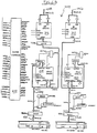
- Figure 7A illustrates the mechanics of the testing operation.
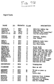
- Figure 7B is a Table of signal designations.
- ITESTP or DTESTP The assertion of the ITESTP or the DTESTP signal by the BIU indicates to the cache unit that testing is underway. This signal (ITESTP or DTESTP) is asserted at the beginning of phase 1 of the stall cycle.
- ITESTP or DTESTP This signal is asserted at the beginning of phase 1 of the stall cycle.
- Block refill (“Mode 2"), both Tag and Data RAMs are written. However, unlike during block refill, the address is generated externally, by the testing agency.
- This feature is present in the ICache to facilitate circuit emulation. It consists of a dedicated (external) pin. When a signal is asserted on this pin, a "miss" is forced whether or not the current instruction access by the CPU is mapped in the ICache. It causes the processor to stall and go external to fetch the instruction. Thus, this feature can be used to interrupt the processor executing out of the cache and force instructions to the CPU from the outside. These external instructions may not be cached. (See Appendix 2 (Module Definition of the Cache Megacell) at page 26.)
Landscapes
- Engineering & Computer Science (AREA)
- Theoretical Computer Science (AREA)
- General Engineering & Computer Science (AREA)
- Physics & Mathematics (AREA)
- General Physics & Mathematics (AREA)
- Computer Hardware Design (AREA)
- Quality & Reliability (AREA)
- Microelectronics & Electronic Packaging (AREA)
- Memory System Of A Hierarchy Structure (AREA)
- Techniques For Improving Reliability Of Storages (AREA)
Applications Claiming Priority (2)
| Application Number | Priority Date | Filing Date | Title |
|---|---|---|---|
| US596986 | 1990-10-12 | ||
| US07/596,986 US5249281A (en) | 1990-10-12 | 1990-10-12 | Testable ram architecture in a microprocessor having embedded cache memory |
Publications (3)
| Publication Number | Publication Date |
|---|---|
| EP0480421A2 true EP0480421A2 (fr) | 1992-04-15 |
| EP0480421A3 EP0480421A3 (en) | 1993-04-21 |
| EP0480421B1 EP0480421B1 (fr) | 1997-07-09 |
Family
ID=24389573
Family Applications (1)
| Application Number | Title | Priority Date | Filing Date |
|---|---|---|---|
| EP91117293A Expired - Lifetime EP0480421B1 (fr) | 1990-10-12 | 1991-10-10 | Architecture de RAM testable dans un microprocesseur ayant une antémémoire encastrée |
Country Status (5)
| Country | Link |
|---|---|
| US (1) | US5249281A (fr) |
| EP (1) | EP0480421B1 (fr) |
| JP (1) | JPH05128000A (fr) |
| KR (1) | KR920008746A (fr) |
| DE (1) | DE69126756T2 (fr) |
Cited By (4)
| Publication number | Priority date | Publication date | Assignee | Title |
|---|---|---|---|---|
| EP0849743A3 (fr) * | 1996-12-19 | 1999-08-04 | Texas Instruments Incorporated | Circuits de mémoire à auto-test incorporés |
| EP1179779A2 (fr) * | 2000-08-07 | 2002-02-13 | Broadcom Corporation | Mode d'accès direct pour une antémémoire |
| WO2004025663A3 (fr) * | 2002-09-11 | 2004-04-29 | Infineon Technologies Ag | Circuit et methode permettant de tester des circuits de memoire vive dynamique (dram) encastree grace a un mode d'acces direct |
| CN116166606A (zh) * | 2023-04-21 | 2023-05-26 | 无锡国芯微高新技术有限公司 | 基于共享紧耦合存储器的高速缓存控制架构 |
Families Citing this family (20)
| Publication number | Priority date | Publication date | Assignee | Title |
|---|---|---|---|---|
| US6446164B1 (en) * | 1991-06-27 | 2002-09-03 | Integrated Device Technology, Inc. | Test mode accessing of an internal cache memory |
| KR100267110B1 (ko) * | 1992-05-28 | 2000-11-01 | 리패치 | 마이크로프로세서에 상주하는 캐시 램을 테스트하는 방법 및 장치 |
| US20030061545A1 (en) * | 1994-09-30 | 2003-03-27 | Chandrashekhar S. Patwardhan | Method and apparatus for providing test mode access to an instruction cache and microcode rom |
| US5900014A (en) * | 1994-12-08 | 1999-05-04 | Ast Research, Inc. | External means of overriding and controlling cacheability attribute of selected CPU accesses to monitor instruction and data streams |
| US5613087A (en) * | 1995-02-23 | 1997-03-18 | International Business Machines Corporation | Cache testing using a modified snoop cycle command |
| US5592616A (en) * | 1995-06-07 | 1997-01-07 | Dell Usa, Lp | Method for performing efficient memory testing on large memory arrays using test code executed from cache memory |
| US5729677A (en) * | 1995-07-31 | 1998-03-17 | Motorola Inc. | Method of testing a cache tag memory array |
| US5768550A (en) * | 1995-11-21 | 1998-06-16 | International Business Machines Corporation | Bus interface logic system |
| US6115789A (en) * | 1997-04-28 | 2000-09-05 | International Business Machines Corporation | Method and system for determining which memory locations have been accessed in a self timed cache architecture |
| US6185703B1 (en) * | 1997-10-10 | 2001-02-06 | Intel Corporation | Method and apparatus for direct access test of embedded memory |
| US5974510A (en) * | 1997-10-31 | 1999-10-26 | Advanced Micro Devices, Inc. | Method for testing the non-cacheable region functioning of a cache memory controller |
| US6240532B1 (en) | 1998-04-06 | 2001-05-29 | Rise Technology Company | Programmable hit and write policy for cache memory test |
| US6367042B1 (en) | 1998-12-11 | 2002-04-02 | Lsi Logic Corporation | Testing methodology for embedded memories using built-in self repair and identification circuitry |
| US6067262A (en) * | 1998-12-11 | 2000-05-23 | Lsi Logic Corporation | Redundancy analysis for embedded memories with built-in self test and built-in self repair |
| US6366990B1 (en) * | 1998-12-14 | 2002-04-02 | Intel Corporation | Method and apparatus for software controlled timing of embedded memory |
| US6651202B1 (en) | 1999-01-26 | 2003-11-18 | Lsi Logic Corporation | Built-in self repair circuitry utilizing permanent record of defects |
| US6421798B1 (en) | 1999-07-14 | 2002-07-16 | Computer Service Technology, Inc. | Chipset-based memory testing for hot-pluggable memory |
| US7007157B2 (en) * | 2001-10-30 | 2006-02-28 | Microsoft Corporation | Network interface sharing methods and apparatuses that support kernel mode data traffic and user mode data traffic |
| JP5267166B2 (ja) * | 2009-01-30 | 2013-08-21 | ソニー株式会社 | インターフェース装置、演算処理装置、インターフェース生成装置、および回路生成装置 |
| US8572449B1 (en) * | 2010-12-20 | 2013-10-29 | Qualcomm Incorporated | Integrated functional testing mechanism for integrated circuits |
Family Cites Families (10)
| Publication number | Priority date | Publication date | Assignee | Title |
|---|---|---|---|---|
| US4161024A (en) * | 1977-12-22 | 1979-07-10 | Honeywell Information Systems Inc. | Private cache-to-CPU interface in a bus oriented data processing system |
| US4575792A (en) * | 1982-03-31 | 1986-03-11 | Honeywell Information Systems Inc. | Shared interface apparatus for testing the memory sections of a cache unit |
| US4562536A (en) * | 1983-06-30 | 1985-12-31 | Honeywell Information Systems Inc. | Directory test error mode control apparatus |
| US4686621A (en) * | 1983-06-30 | 1987-08-11 | Honeywell Information Systems Inc. | Test apparatus for testing a multilevel cache system with graceful degradation capability |
| JPH0630075B2 (ja) * | 1984-08-31 | 1994-04-20 | 株式会社日立製作所 | キャッシュメモリを有するデータ処理装置 |
| US4744049A (en) * | 1984-10-15 | 1988-05-10 | Motorola, Inc. | Microcode testing of a cache in a data processor |
| JP2583525B2 (ja) * | 1987-09-30 | 1997-02-19 | 健 坂村 | データ処理装置 |
| US4882673A (en) * | 1987-10-02 | 1989-11-21 | Advanced Micro Devices, Inc. | Method and apparatus for testing an integrated circuit including a microprocessor and an instruction cache |
| US4937781A (en) * | 1988-05-13 | 1990-06-26 | Dallas Semiconductor Corporation | Dual port ram with arbitration status register |
| US4945512A (en) * | 1988-09-07 | 1990-07-31 | Unisys Corporation | High-speed partitioned set associative cache memory |
-
1990
- 1990-10-12 US US07/596,986 patent/US5249281A/en not_active Expired - Fee Related
-
1991
- 1991-10-09 JP JP3290712A patent/JPH05128000A/ja active Pending
- 1991-10-10 DE DE69126756T patent/DE69126756T2/de not_active Expired - Fee Related
- 1991-10-10 EP EP91117293A patent/EP0480421B1/fr not_active Expired - Lifetime
- 1991-10-12 KR KR1019910017947A patent/KR920008746A/ko not_active Withdrawn
Cited By (5)
| Publication number | Priority date | Publication date | Assignee | Title |
|---|---|---|---|---|
| EP0849743A3 (fr) * | 1996-12-19 | 1999-08-04 | Texas Instruments Incorporated | Circuits de mémoire à auto-test incorporés |
| EP1179779A2 (fr) * | 2000-08-07 | 2002-02-13 | Broadcom Corporation | Mode d'accès direct pour une antémémoire |
| WO2004025663A3 (fr) * | 2002-09-11 | 2004-04-29 | Infineon Technologies Ag | Circuit et methode permettant de tester des circuits de memoire vive dynamique (dram) encastree grace a un mode d'acces direct |
| US7171596B2 (en) | 2002-09-11 | 2007-01-30 | Infineon Technologies Ag | Circuit and method for testing embedded DRAM circuits through direct access mode |
| CN116166606A (zh) * | 2023-04-21 | 2023-05-26 | 无锡国芯微高新技术有限公司 | 基于共享紧耦合存储器的高速缓存控制架构 |
Also Published As
| Publication number | Publication date |
|---|---|
| EP0480421A3 (en) | 1993-04-21 |
| JPH05128000A (ja) | 1993-05-25 |
| DE69126756D1 (de) | 1997-08-14 |
| DE69126756T2 (de) | 1998-01-29 |
| KR920008746A (ko) | 1992-05-28 |
| US5249281A (en) | 1993-09-28 |
| EP0480421B1 (fr) | 1997-07-09 |
Similar Documents
| Publication | Publication Date | Title |
|---|---|---|
| US5249281A (en) | Testable ram architecture in a microprocessor having embedded cache memory | |
| US5519839A (en) | Double buffering operations between the memory bus and the expansion bus of a computer system | |
| US5793941A (en) | On-chip primary cache testing circuit and test method | |
| EP0636973B1 (fr) | Puce interface pour système à double microprocesseur | |
| US5745732A (en) | Computer system including system controller with a write buffer and plural read buffers for decoupled busses | |
| US5996048A (en) | Inclusion vector architecture for a level two cache | |
| US4899275A (en) | Cache-MMU system | |
| US5809280A (en) | Adaptive ahead FIFO with LRU replacement | |
| US5091846A (en) | Cache providing caching/non-caching write-through and copyback modes for virtual addresses and including bus snooping to maintain coherency | |
| US5276833A (en) | Data cache management system with test mode using index registers and CAS disable and posted write disable | |
| US4933835A (en) | Apparatus for maintaining consistency of a cache memory with a primary memory | |
| US5581727A (en) | Hierarchical cache system flushing scheme based on monitoring and decoding processor bus cycles for flush/clear sequence control | |
| US4860192A (en) | Quadword boundary cache system | |
| US5255384A (en) | Memory address translation system having modifiable and non-modifiable translation mechanisms | |
| US5809524A (en) | Method and apparatus for cache memory replacement line identification | |
| US7051239B2 (en) | Method and apparatus for efficiently implementing trace and/or logic analysis mechanisms on a processor chip | |
| US5787486A (en) | Bus protocol for locked cycle cache hit | |
| US4884197A (en) | Method and apparatus for addressing a cache memory | |
| US5809530A (en) | Method and apparatus for processing multiple cache misses using reload folding and store merging | |
| US5642494A (en) | Cache memory with reduced request-blocking | |
| US5636363A (en) | Hardware control structure and method for off-chip monitoring entries of an on-chip cache | |
| US5161162A (en) | Method and apparatus for system bus testability through loopback | |
| US5860105A (en) | NDIRTY cache line lookahead | |
| US6446164B1 (en) | Test mode accessing of an internal cache memory | |
| WO1996035995A1 (fr) | Procede et appareil permettant de gerer des demandes d'espionnage a l'aide de cellules consultatives d'espionnage |
Legal Events
| Date | Code | Title | Description |
|---|---|---|---|
| PUAI | Public reference made under article 153(3) epc to a published international application that has entered the european phase |
Free format text: ORIGINAL CODE: 0009012 |
|
| AK | Designated contracting states |
Kind code of ref document: A2 Designated state(s): DE FR GB IT NL |
|
| PUAL | Search report despatched |
Free format text: ORIGINAL CODE: 0009013 |
|
| AK | Designated contracting states |
Kind code of ref document: A3 Designated state(s): DE FR GB IT NL |
|
| 17P | Request for examination filed |
Effective date: 19931021 |
|
| 17Q | First examination report despatched |
Effective date: 19951227 |
|
| GRAG | Despatch of communication of intention to grant |
Free format text: ORIGINAL CODE: EPIDOS AGRA |
|
| GRAH | Despatch of communication of intention to grant a patent |
Free format text: ORIGINAL CODE: EPIDOS IGRA |
|
| GRAH | Despatch of communication of intention to grant a patent |
Free format text: ORIGINAL CODE: EPIDOS IGRA |
|
| GRAA | (expected) grant |
Free format text: ORIGINAL CODE: 0009210 |
|
| AK | Designated contracting states |
Kind code of ref document: B1 Designated state(s): DE FR GB IT NL |
|
| REF | Corresponds to: |
Ref document number: 69126756 Country of ref document: DE Date of ref document: 19970814 |
|
| ET | Fr: translation filed | ||
| ITF | It: translation for a ep patent filed | ||
| PGFP | Annual fee paid to national office [announced via postgrant information from national office to epo] |
Ref country code: FR Payment date: 19970918 Year of fee payment: 7 Ref country code: NL Payment date: 19970918 Year of fee payment: 7 |
|
| PGFP | Annual fee paid to national office [announced via postgrant information from national office to epo] |
Ref country code: DE Payment date: 19970925 Year of fee payment: 7 |
|
| PLBE | No opposition filed within time limit |
Free format text: ORIGINAL CODE: 0009261 |
|
| STAA | Information on the status of an ep patent application or granted ep patent |
Free format text: STATUS: NO OPPOSITION FILED WITHIN TIME LIMIT |
|
| 26N | No opposition filed | ||
| PG25 | Lapsed in a contracting state [announced via postgrant information from national office to epo] |
Ref country code: NL Free format text: LAPSE BECAUSE OF NON-PAYMENT OF DUE FEES Effective date: 19990501 |
|
| PG25 | Lapsed in a contracting state [announced via postgrant information from national office to epo] |
Ref country code: FR Free format text: LAPSE BECAUSE OF NON-PAYMENT OF DUE FEES Effective date: 19990630 |
|
| NLV4 | Nl: lapsed or anulled due to non-payment of the annual fee |
Effective date: 19990501 |
|
| REG | Reference to a national code |
Ref country code: FR Ref legal event code: ST |
|
| PG25 | Lapsed in a contracting state [announced via postgrant information from national office to epo] |
Ref country code: DE Free format text: LAPSE BECAUSE OF NON-PAYMENT OF DUE FEES Effective date: 19990803 |
|
| REG | Reference to a national code |
Ref country code: GB Ref legal event code: IF02 |
|
| PGFP | Annual fee paid to national office [announced via postgrant information from national office to epo] |
Ref country code: GB Payment date: 20051005 Year of fee payment: 15 |
|
| PG25 | Lapsed in a contracting state [announced via postgrant information from national office to epo] |
Ref country code: IT Free format text: LAPSE BECAUSE OF NON-PAYMENT OF DUE FEES;WARNING: LAPSES OF ITALIAN PATENTS WITH EFFECTIVE DATE BEFORE 2007 MAY HAVE OCCURRED AT ANY TIME BEFORE 2007. THE CORRECT EFFECTIVE DATE MAY BE DIFFERENT FROM THE ONE RECORDED. Effective date: 20051010 |
|
| GBPC | Gb: european patent ceased through non-payment of renewal fee |
Effective date: 20061010 |
|
| PG25 | Lapsed in a contracting state [announced via postgrant information from national office to epo] |
Ref country code: GB Free format text: LAPSE BECAUSE OF NON-PAYMENT OF DUE FEES Effective date: 20061010 |