EP0480500B1 - Transistor à effet de champ à tension de seuil répartie - Google Patents
Transistor à effet de champ à tension de seuil répartie Download PDFInfo
- Publication number
- EP0480500B1 EP0480500B1 EP91202497A EP91202497A EP0480500B1 EP 0480500 B1 EP0480500 B1 EP 0480500B1 EP 91202497 A EP91202497 A EP 91202497A EP 91202497 A EP91202497 A EP 91202497A EP 0480500 B1 EP0480500 B1 EP 0480500B1
- Authority
- EP
- European Patent Office
- Prior art keywords
- effect transistor
- field effect
- gate
- gate electrode
- semiconductor layer
- Prior art date
- Legal status (The legal status is an assumption and is not a legal conclusion. Google has not performed a legal analysis and makes no representation as to the accuracy of the status listed.)
- Expired - Lifetime
Links
- 230000005669 field effect Effects 0.000 title claims description 41
- 239000012212 insulator Substances 0.000 claims description 39
- 239000004065 semiconductor Substances 0.000 claims description 33
- 239000003990 capacitor Substances 0.000 claims description 20
- 230000000694 effects Effects 0.000 claims description 18
- 239000000758 substrate Substances 0.000 claims description 6
- 230000001052 transient effect Effects 0.000 description 27
- 229910021417 amorphous silicon Inorganic materials 0.000 description 13
- 239000011159 matrix material Substances 0.000 description 8
- 238000000034 method Methods 0.000 description 6
- 238000009825 accumulation Methods 0.000 description 5
- 238000004519 manufacturing process Methods 0.000 description 5
- 229910004205 SiNX Inorganic materials 0.000 description 4
- 239000004973 liquid crystal related substance Substances 0.000 description 3
- IUVCFHHAEHNCFT-INIZCTEOSA-N 2-[(1s)-1-[4-amino-3-(3-fluoro-4-propan-2-yloxyphenyl)pyrazolo[3,4-d]pyrimidin-1-yl]ethyl]-6-fluoro-3-(3-fluorophenyl)chromen-4-one Chemical compound C1=C(F)C(OC(C)C)=CC=C1C(C1=C(N)N=CN=C11)=NN1[C@@H](C)C1=C(C=2C=C(F)C=CC=2)C(=O)C2=CC(F)=CC=C2O1 IUVCFHHAEHNCFT-INIZCTEOSA-N 0.000 description 2
- 238000009826 distribution Methods 0.000 description 2
- 239000011521 glass Substances 0.000 description 2
- 238000000926 separation method Methods 0.000 description 2
- 229910052581 Si3N4 Inorganic materials 0.000 description 1
- 230000015556 catabolic process Effects 0.000 description 1
- 238000006731 degradation reaction Methods 0.000 description 1
- 229910052751 metal Inorganic materials 0.000 description 1
- 239000002184 metal Substances 0.000 description 1
- 150000002739 metals Chemical class 0.000 description 1
- 238000009828 non-uniform distribution Methods 0.000 description 1
- 230000003287 optical effect Effects 0.000 description 1
- 229910021420 polycrystalline silicon Inorganic materials 0.000 description 1
- HQVNEWCFYHHQES-UHFFFAOYSA-N silicon nitride Chemical compound N12[Si]34N5[Si]62N3[Si]51N64 HQVNEWCFYHHQES-UHFFFAOYSA-N 0.000 description 1
- 239000010409 thin film Substances 0.000 description 1
- 230000036962 time dependent Effects 0.000 description 1
Images

Classifications
-
- H—ELECTRICITY
- H10—SEMICONDUCTOR DEVICES; ELECTRIC SOLID-STATE DEVICES NOT OTHERWISE PROVIDED FOR
- H10D—INORGANIC ELECTRIC SEMICONDUCTOR DEVICES
- H10D86/00—Integrated devices formed in or on insulating or conducting substrates, e.g. formed in silicon-on-insulator [SOI] substrates or on stainless steel or glass substrates
Definitions
- the invention relates to a distributed threshold voltage field effect transistor (DTV-FET) wherein a first field effect transistor (FET) and a second FET are coupled in series and a voltage is applied to the gate of the first FET.
- DTV-FET distributed threshold voltage field effect transistor
- a low off-current is a very important factor for amorphous-silicon field-effect transistors (a-Si FETs) used in active matrices. This is because a high off-current causes various problems in FET-addressed liquid-crystal displays, such as degradation of optical image quality.
- a-Si FETs amorphous-silicon field-effect transistors
- DTV-FET Distributed Threshold Voltage Field Effect Transistor
- This freedom can be used for instance to counter a non-uniform distribution of transistor characteristics within an active matrix, or to increase the choice of liquid crystals that can be used. Also, the reduction in off current that occurs as a result of the DTV-FET effect leads to an improved performance of active matrix LCD displays.
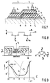
- the simplest way to realize the DTV-FET is, as shown in Fig. 8, to externally connect two normal transistors in series and apply the gate voltage Vg plus a constant offset voltage Vos to the transistor on the drain side.
- a second method to fabricate the DTV-FET is, as shown in Fig. 9a, to dope part of the channel.
- the channel region denoted "n ⁇ a-Si" is nominally undoped, but the region denoted "n a-Si” is moderately doped.
- the effect of the doping is to shift the characteristics (in gate voltage terms) without altering their shape.
- the threshold voltage distribution is a step function along the channel. This then results in the DTV-FET effect.
- Fig. 9b shows an equivalent circuit of the DTV-FET shown in Fig. 9a which is formed by connecting two uniform FETs, Q s and Q d , in series.
- Fig. 9c shows one example of off-characteristics of DTV-FET shown in Fig. 9a wherein the dotted curves are those of the individual uniform FETs.
- the DTV-FET structures proposed so far achieve the DTV-FET effect either by using an extra offset voltage as DTV-FET in Fig. 8 or by doping part of the channel as one in Fig. 9a.
- the disadvantage of the first method is that it requires application of at least a third voltage to what is in effect a four terminal device.
- the fabrication of these additional scan lines increases production cost an their presence increases the chance of display failure due to, for example, cross-over shorts.
- the area occupied by the additional scan lines reduces the display's aperture ratio.
- the second method of creating the DTV-FET by doping part of the channel avoids the need for an extra voltage and the problem of the additional scan lines.
- the amplitude of the distribution in VT and therefore the magnitude of the DTV-FET effect is limited by the relatively small shift in threshold voltage that can be obtained by doping (see, for example, Uchida and Matsumura, MRS Symp Proc. 149 247 (1989).
- the DTV-FET according to the invention is characterized in that
- the invention is based on the following recognition.
- the transistors always operate under pulsed driving conditions. It is therefore possible to use RC circuits to create temporary offset voltages between two or more gates, which will be explained with Figs. 4a and 4b.
- a pulsed wave form as shown in Fig. 4b is applied at node 1 and appears unchanged at node 2.
- the time constant of RC circuit 3 is of the same order as either t on or t off , a time dependent voltage will appear between node 2 and node 4.
- a non-linear device such as, for example, a diode for the resistance in the RC circuit, these offset voltages can be made to depend on whether the device is in an "on" or in an "off” stage.
- the DTV-FET can be obtained by connecting node 2 to the gate of a first field effect transistor which constitutes a main gate and node 4 to the gate of a second field effect transistor which constitutes a transient gate.
- the other one of the symmetrical DTV-FETs is characterized in that another field effect transistor whose gate is coupled to the first field effect transistor is coupled to the second field effect transistor in series.
- the non-linear resistor is a diode in the DTV-FET.
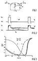
- Figure 1 illustrates the DTV-FET of the present invention based on the above-mentioned recognition.
- the main gate potential Vg at node 5 is a pulsed drive form as illustrated in Figure 2.
- the circuit is required to work in an n-channel mode, i.e. the on voltage V on is larger than the off voltage V off .
- a similar description can also be made using the reverse condition of p-channel transistors and an inverted gate voltage wave form.
- the potential illustrated in the upper waveform of Figure 2 is applied directly to a main gate, the gate of transistor 6.
- the gate potential Vg′ of transistor 7, a transient gate potential, is determined by the RC circuit of capacitors 8 and 9 and non-linear resistor 10.
- This non-linear resistor has the property that when node 30 is negative with respect to node 5, its resistivity has a low value R on , but when the voltage difference across non-linear resistor 10 is positive, its resistivity has a large value R off .
- the non-linear resistor 10 can be fabricated by a diode, a transistor, etc.
- C1, C2, R on and R off are chosen in relation to t on and t off such that: (1) R on (C1+C2) ⁇ ⁇ t on (2) R off (C1+C2) > > t off
- the DTV-FET effect of the circuit device in Figure 1 is illustrated in Figure 3.
- This curve a represents in effect the conventional (non DTV-FET) transistor.
- Curve b shows the characteristic if the gate of transistor 6 is also connected to Vg′.
- FIGs 5a and 5b show modified embodiments of the DTV-FET of Figure 1 which are essential if such device is to be applied to active matrix displays.
- operation under both negative and positive drain voltage is required, which needs a symmetrical DTV-FET.
- a transient gate must also be created under the source contact, or a normal transistor placed at the drain contact.
- an extra transistor 13 has been added on the left, the gate of this extra transistor is connected to the transient gate potential Vg'.
- the extra transistor 13 is placed on the right and its gate connected to the gate potential Vg.
- the strict distinction between source and drain disappears and the circuits will show a DTV-FET effect for both a negative and a positive potential difference between contacts 14 and 15.
- the circuit in Figure 1 can, of course, be realized by using standard components like discrete FETs and capacitors.
- the area occupied by the different components and the extra fabrication steps required to provide inter connections between them will decrease the display aperture, increase production cost, and decrease yield.
- FIG. 6 Shown in Figure 6 is an example of the DTV-FET structure according to the present invention.
- substrate 26 On substrate 26 of, for example, glass, is provided gate electrode 16 of, for example Cr.
- This gate electrode 16 is partially covered by first insulator layer 17 of, for example SiNx, and partly covered by second insulator layer 19, also of, for example SiNx.
- the transient gate electrode 18 of, for example Mo is provided on top of first insulator layer 17 and covered by second insulator layer 19 except for a window which has been provided to give electrical contact between transient gate electrode 18 and contact 21.
- semiconductor layer 20 On top of second insulator layer 19 is provided semiconductor layer 20 of, for example a-Si:H and contacts 21, 22, 23, 24 and 25 of, for example A1, are provided on semiconductor layer 20.
- Transistor 6 in Figure 1 is comprised in region T1 of gate electrode 16 as gate, second insulator layer 19 as gate dielectric, semiconductor layer 20 as active layer, and contacts 23 and 24 as source and drain respectively.
- the transistor 7 in Figure 1 is comprised in region T2 of transient gate electrode 18 as gate, second insulator layer 19 as gate dielectric, semiconductor layer 20 as active layer and contacts 24 and 25 as source and drain respectively.
- Capacitor 8 in Figure 1 is comprised in region T2 of gate electrode 16 as bottom plate, first insulator layer 17 as dielectric and transient gate electrode 18 as top plate.
- capacitor 9 in Figure 1 is comprised in region T2 of transient gate electrode 18 as bottom plate, second insulator layer 19 as dielectric and semiconductor layer 20 as a top capacitor plate.
- contact 24 which acts as drain for transistor 6 and as source for transistor 7, is to provide a connection between the regions of the active layer 20 in which the channels of transistors 6 and 7 are located and to bridge the region where the first insulator layer is not covered by transient gate 18.
- the length of contact 24 is determined by the length of this latter region and will be zero if this region does not exist.
- potential Vg is applied to gate electrode 16, potential Vs to contact 23 and potential Vd to contact 25 as shown in Figure 6.
- non-linear resistor element 10 in Figure 1 is provided by the transistor in region T3 which comprises gate electrode 16 as gate, second insulator layer 19 as gate dielectric, semiconductor layer 20 as active layer, source contact 21 and drain contact 22. Gate and drain of this transistor are electrically connected, and this transistor represents a low resistivity R on between gate electrode 16 and transient electrode 18 when the gate potential is at V on , and a high resistivity R off when the gate potential is at V off .
- the transconductance function used to calculate the results in Figure 3 was based on an inverted staggered amorphous silicon thin film transistors T1, T2, with a 2100 A thick silicon nitride gate insulator layers 17, 19, an active layer 20 thickness of 800 A and A1 source and drain contacts 21-25.
- the aspect ratio W/L was 10.
- a second structure of the DTV-FET according to the present invention is shown in Figure 7.
- substrate 26 of, for example, glass
- gate electrode 16 of, for example, Cr which is partly covered by first insulator layer 17 of, for example SiNx.
- transient gate 18 covers both first insulator layer 17 and part of the gate electrode 16. Furthermore, transient gate 18 is a semiconductor, for example p-type a-Si:H, of the opposite conductive type of the conductive type of the channel in active layer 20, which is for example, n-channel conduction in a-Si:H. Second insulator layer 19 of, for example, SiNx and active layer 20 are layered on top of transient gate 18.
- potential Vg is applied to gate electrode 16, potential Vs to contact 23 and potential Vd to contact 25.
- transistor 6 is comprised in region T1 of the portion of the transient gate electrode 18 which lies directly on gate electrode 16 as gate, second insulator 19 as gate dielectric, semiconductor layer 20 as active layer, contact 23 as source and the middle of the active layer 20 as virtual drain.
- Transistor 7 is comprised in region T2 of the portion of transient gate electrode 18 sandwiched between the first and second insulator layers 17, 19 as gate, second insulator layer 19 as gate dielectric, semiconductor layer 20 as active layer, contact 25 as drain and the middle of active layer 20 as virtual source.
- Capacitor 8 is provided in region C1 shown in Figure 7 by gate electrode 16 as bottom plate, first insulator layer 17 as dielectric and the portion of transient gate layer 18 sandwiched by the first and second insulator layers 17, 19, as a top plate.
- Capacitor 9 is, as shown in region C2 in Figure 7, build up out of the same part of transient gate 18 as bottom plate, second insulator layer 19 as gate dielectric and finally active layer 20 as a top plate.
- Non-linear resistor element 10 in Figure 1, shown in NL in Figure 7, is provided by transient gate layer 18 itself.
- the difference in R on and R off of this doped semiconductor layer derives from the difference in hole and electron conduction within this layer.
- the channel of the transistor in active layer 20 is of an electron enhancement type and the conductive type of the transient gate is therefore p-type, then during the on-time t on the gate potential Vg will be such that a positive potential difference exists between transient gate 18 and active layer 20.
- This potential difference results in an electron accumulation channel in the active layer as intended, but it also induces a hole accumulation in the transient gate.
- This hole accumulation causes a low resistance R on between the portion of the transient gate sandwiched between the first and second insulator layer in region T2 and the portion of the transient gate which lies directly on the main gate in region T1.
- the elements building up capacitor 9 and transistor 7 are identical. Furthermore, it is recognized that because the top plate of capacitor 9 is formed by active layer 20, the top plate of capacitor 9 is not at a single potential but changes continuously between the potential of contact 25 on the right hand side, to the potential of contact 24 on the left hand side in the case of Figure 6, and the potential of the middle of active layer 20 in the case of Figure 7.
- the A1 contacts are applied directly onto the semiconductor layer, however, in present a-Si:H TFT technology, n+-type doped semiconductor layers and layers of alternative metals like Cr are sometimes inserted between the a-Si:H semiconductor and the A1. Such added features and process steps are not precluded by this invention.
Landscapes
- Thin Film Transistor (AREA)
- Metal-Oxide And Bipolar Metal-Oxide Semiconductor Integrated Circuits (AREA)
Claims (6)
- Transistor à effet de champ à tension de seuil répartie, dans lequel un premier transistor à effet de champ et un deuxième transistor à effet de champ sont couplés en série et une tension est appliquée à la grille du premier transistor à effet de champ, caractérisé en ce que(a) la tension est une tension à impulsions dont le temps à l'état passant et le temps à l'état bloqué sont respectivement ton et toff;(b) un premier condensateur de capacité C₁ et un deuxième condensateur de capacité C₂ sont couplés en série entre le point de jonction du premier transistor à effet de champ et le deuxième transistor à effet de champ et la grille du premier transistor à effet de champ;(c) une résistance non linéaire, dont la résistivité est Ron pendant ton et Roff pendant toff, est couplée entre les grilles respectives du premier transistor à effet de champ et du deuxième transistor à effet de champ;(d) le point de jonction du premier condensateur et du deuxième condensateur est couplé à la grille du deuxième transistor à effet de champ;(e) la constante de temps Ron(C₁+C₂) est suffisamment plus petite que ton, et(f) la constante de temps Roff(C₁+C₂) est suffisamment plus grande que toff pour qu'une tension polarisée soit formée sur la grille du deuxième transistor à effet de champ pendant toff.
- Transistor à effet de champ à tension de seuil répartie selon la revendication 1, caractérisé en ce qu'un autre transistor à effet de champ, dont la grille est couplée au deuxième transistor à effet de champ, est couplé en série au premier transistor à effet de champ.
- Transistor à effet de champ à tension de seuil répartie selon la revendication 1, caractérisé en ce qu'un autre transistor à effet de champ, dont la grille est couplée au premier transistor à effet de champ, est couplé en série au deuxième transistor à effet de champ.
- Transistor à effet de champ à tension de seuil répartie selon l'une quelconque des revendications 1 à 3, caractérisé en ce que la résistance non linéaire est une diode.
- Transistor à effet de champ à tension de seuil répartie selon l'une quelconque des revendications précédentes, caractérisé en ce qu'il comprend:(a) une première électrode de grille prévue sur un substrat;(b) une première couche d'isolateur recouvrant partiellement l'électrode de grille;(c) une deuxième électrode de grille prévue sur la première couche d'isolateur;(d) une deuxième couche d'isolateur recouvrant la première électrode de grille et la deuxième électrode de grille à l'exception d'une fenêtre ménagée sur la deuxième électrode de grille;(e) une couche à semi-conducteurs prévue sur la deuxième couche d'isolateur;(f) deux contacts prévus sur une partie de la couche à semi-conducteurs, et(g) deux contacts prévus sur l'autre partie de la deuxième couche d'isolateur, dont l'un est raccordé entre la couche à semi-conducteurs et la deuxième électrode de grille, et l'autre est raccordé entre la couche à semiconducteurs et la première électrode de grille.
- Transistor à effet de champ à tension de seuil répartie selon l'une quelconque des revendications 1 à 4, caractérisé en ce qu'il comprend :(a) une électrode de grille prévue sur un substrat;(b) une première couche d'isolateur recouvrant partiellement l'électrode de grille;(c) une première couche à semi-conducteurs recouvrant à la fois la première couche d'isolateur et une partie de l'électrode de grille;(d) une deuxième couche d'isolateur prévue sur la première couche à semi-conducteurs;(e) une deuxième couche à semi-conducteurs dont le type conducteur du canal est opposé à celui de la première couche à semi-conducteurs, et(f) deux contacts prévus sur la deuxième couche à semi-conducteurs.
Applications Claiming Priority (2)
| Application Number | Priority Date | Filing Date | Title |
|---|---|---|---|
| JP2267237A JPH04144166A (ja) | 1990-10-04 | 1990-10-04 | 分布しきい値型電界効果トランジスタ |
| JP267237/90 | 1990-10-04 |
Publications (2)
| Publication Number | Publication Date |
|---|---|
| EP0480500A1 EP0480500A1 (fr) | 1992-04-15 |
| EP0480500B1 true EP0480500B1 (fr) | 1995-08-30 |
Family
ID=17442044
Family Applications (1)
| Application Number | Title | Priority Date | Filing Date |
|---|---|---|---|
| EP91202497A Expired - Lifetime EP0480500B1 (fr) | 1990-10-04 | 1991-09-26 | Transistor à effet de champ à tension de seuil répartie |
Country Status (4)
| Country | Link |
|---|---|
| US (1) | US5266820A (fr) |
| EP (1) | EP0480500B1 (fr) |
| JP (1) | JPH04144166A (fr) |
| DE (1) | DE69112561T2 (fr) |
Families Citing this family (6)
| Publication number | Priority date | Publication date | Assignee | Title |
|---|---|---|---|---|
| WO1995031043A2 (fr) * | 1994-05-06 | 1995-11-16 | Philips Electronics N.V. | Composant semi-conducteur de totalisaiton d'une pluralite de signaux d'entree ponderes |
| US5763924A (en) * | 1996-05-09 | 1998-06-09 | Linear Technology Corporation | Circuits and methods for compensating non-linear capacitances to minimize harmonic distortion |
| JPH10116964A (ja) | 1996-10-09 | 1998-05-06 | Oki Electric Ind Co Ltd | 半導体装置とその製造方法およびスパッタリング装置 |
| US6507044B1 (en) * | 1999-03-25 | 2003-01-14 | Advanced Micro Devices, Inc. | Position-selective and material-selective silicon etching to form measurement structures for semiconductor fabrication |
| US10347667B2 (en) * | 2017-07-26 | 2019-07-09 | International Business Machines Corporation | Thin-film negative differential resistance and neuronal circuit |
| CN116500774B (zh) * | 2022-01-19 | 2023-10-31 | 荣耀终端有限公司 | 电润湿基板、电润湿显示面板及电润湿显示装置 |
Family Cites Families (2)
| Publication number | Priority date | Publication date | Assignee | Title |
|---|---|---|---|---|
| JPS599735A (ja) * | 1982-07-07 | 1984-01-19 | Mitsubishi Electric Corp | クロツク発生回路 |
| US5113091A (en) * | 1988-05-20 | 1992-05-12 | Texas Instruments Incorporated | Apparatus and method for comparing signals |
-
1990
- 1990-10-04 JP JP2267237A patent/JPH04144166A/ja active Pending
-
1991
- 1991-09-26 EP EP91202497A patent/EP0480500B1/fr not_active Expired - Lifetime
- 1991-09-26 DE DE69112561T patent/DE69112561T2/de not_active Expired - Fee Related
- 1991-09-30 US US07/769,919 patent/US5266820A/en not_active Expired - Fee Related
Also Published As
| Publication number | Publication date |
|---|---|
| JPH04144166A (ja) | 1992-05-18 |
| EP0480500A1 (fr) | 1992-04-15 |
| US5266820A (en) | 1993-11-30 |
| DE69112561T2 (de) | 1996-04-18 |
| DE69112561D1 (de) | 1995-10-05 |
Similar Documents
| Publication | Publication Date | Title |
|---|---|---|
| KR100488641B1 (ko) | 반도체 집적 회로 | |
| US5124769A (en) | Thin film transistor | |
| KR950003943B1 (ko) | 박막 반도체 장치 | |
| US7189992B2 (en) | Transistor structures having a transparent channel | |
| US5583366A (en) | Active matrix panel | |
| US5362979A (en) | SOI transistor with improved source-high performance | |
| KR100373940B1 (ko) | 박막반도체장치 | |
| US3855610A (en) | Semiconductor device | |
| US6411348B2 (en) | Active matrix substrate and producing method of the same | |
| US5017983A (en) | Amorphous silicon thin film transistor with a depletion gate | |
| US4404578A (en) | Structure of thin film transistors | |
| US5144392A (en) | Thin-film transistor circuit | |
| CA1160760A (fr) | Condensateur a effet de champ | |
| US5038184A (en) | Thin film varactors | |
| US5266820A (en) | Distributed threshold voltage field effect transistor | |
| US6100565A (en) | Semiconductor integrated circuit device with operation in partial depletion type mode and perfect depletion type mode | |
| KR100418642B1 (ko) | Soi 반도체장치 및 그 제조방법 | |
| US4998146A (en) | High voltage thin film transistor | |
| KR100326832B1 (ko) | 고전압 박막 트랜지스터 및 그 제조방법 | |
| US5329140A (en) | Thin film transistor and its production method | |
| JP3401918B2 (ja) | 半導体装置 | |
| US6392623B1 (en) | Method for driving active matrix substrate and liquid crystal display device using the same | |
| KR940008220B1 (ko) | 박막트랜지스터 | |
| KR100225100B1 (ko) | 박막트랜지스터 | |
| JP3503197B2 (ja) | 半導体装置 |
Legal Events
| Date | Code | Title | Description |
|---|---|---|---|
| PUAI | Public reference made under article 153(3) epc to a published international application that has entered the european phase |
Free format text: ORIGINAL CODE: 0009012 |
|
| AK | Designated contracting states |
Kind code of ref document: A1 Designated state(s): DE FR GB NL |
|
| 17P | Request for examination filed |
Effective date: 19920924 |
|
| 17Q | First examination report despatched |
Effective date: 19941018 |
|
| GRAA | (expected) grant |
Free format text: ORIGINAL CODE: 0009210 |
|
| AK | Designated contracting states |
Kind code of ref document: B1 Designated state(s): DE FR GB NL |
|
| PG25 | Lapsed in a contracting state [announced via postgrant information from national office to epo] |
Ref country code: NL Free format text: LAPSE BECAUSE OF NON-PAYMENT OF DUE FEES Effective date: 19950830 |
|
| REF | Corresponds to: |
Ref document number: 69112561 Country of ref document: DE Date of ref document: 19951005 |
|
| ET | Fr: translation filed | ||
| NLV1 | Nl: lapsed or annulled due to failure to fulfill the requirements of art. 29p and 29m of the patents act | ||
| PLBE | No opposition filed within time limit |
Free format text: ORIGINAL CODE: 0009261 |
|
| STAA | Information on the status of an ep patent application or granted ep patent |
Free format text: STATUS: NO OPPOSITION FILED WITHIN TIME LIMIT |
|
| 26N | No opposition filed | ||
| PGFP | Annual fee paid to national office [announced via postgrant information from national office to epo] |
Ref country code: GB Payment date: 19970829 Year of fee payment: 7 |
|
| PGFP | Annual fee paid to national office [announced via postgrant information from national office to epo] |
Ref country code: FR Payment date: 19970923 Year of fee payment: 7 |
|
| PGFP | Annual fee paid to national office [announced via postgrant information from national office to epo] |
Ref country code: DE Payment date: 19971121 Year of fee payment: 7 |
|
| REG | Reference to a national code |
Ref country code: FR Ref legal event code: CD |
|
| PG25 | Lapsed in a contracting state [announced via postgrant information from national office to epo] |
Ref country code: GB Free format text: LAPSE BECAUSE OF NON-PAYMENT OF DUE FEES Effective date: 19980926 |
|
| GBPC | Gb: european patent ceased through non-payment of renewal fee |
Effective date: 19980926 |
|
| PG25 | Lapsed in a contracting state [announced via postgrant information from national office to epo] |
Ref country code: FR Free format text: LAPSE BECAUSE OF NON-PAYMENT OF DUE FEES Effective date: 19990531 |
|
| PG25 | Lapsed in a contracting state [announced via postgrant information from national office to epo] |
Ref country code: DE Free format text: LAPSE BECAUSE OF NON-PAYMENT OF DUE FEES Effective date: 19990701 |
|
| REG | Reference to a national code |
Ref country code: FR Ref legal event code: ST |