EP0480703A2 - La formation de configurations de métal sur un substrat - Google Patents
La formation de configurations de métal sur un substrat Download PDFInfo
- Publication number
- EP0480703A2 EP0480703A2 EP91309278A EP91309278A EP0480703A2 EP 0480703 A2 EP0480703 A2 EP 0480703A2 EP 91309278 A EP91309278 A EP 91309278A EP 91309278 A EP91309278 A EP 91309278A EP 0480703 A2 EP0480703 A2 EP 0480703A2
- Authority
- EP
- European Patent Office
- Prior art keywords
- metal
- layer
- substrate
- titanium
- depositing
- Prior art date
- Legal status (The legal status is an assumption and is not a legal conclusion. Google has not performed a legal analysis and makes no representation as to the accuracy of the status listed.)
- Granted
Links
Images


Classifications
-
- H—ELECTRICITY
- H05—ELECTRIC TECHNIQUES NOT OTHERWISE PROVIDED FOR
- H05K—PRINTED CIRCUITS; CASINGS OR CONSTRUCTIONAL DETAILS OF ELECTRIC APPARATUS; MANUFACTURE OF ASSEMBLAGES OF ELECTRICAL COMPONENTS
- H05K3/00—Apparatus or processes for manufacturing printed circuits
- H05K3/22—Secondary treatment of printed circuits
- H05K3/225—Correcting or repairing of printed circuits
-
- B—PERFORMING OPERATIONS; TRANSPORTING
- B23—MACHINE TOOLS; METAL-WORKING NOT OTHERWISE PROVIDED FOR
- B23K—SOLDERING OR UNSOLDERING; WELDING; CLADDING OR PLATING BY SOLDERING OR WELDING; CUTTING BY APPLYING HEAT LOCALLY, e.g. FLAME CUTTING; WORKING BY LASER BEAM
- B23K26/00—Working by laser beam, e.g. welding, cutting or boring
- B23K26/36—Removing material
- B23K26/40—Removing material taking account of the properties of the material involved
-
- H—ELECTRICITY
- H01—ELECTRIC ELEMENTS
- H01C—RESISTORS
- H01C17/00—Apparatus or processes specially adapted for manufacturing resistors
- H01C17/22—Apparatus or processes specially adapted for manufacturing resistors adapted for trimming
- H01C17/24—Apparatus or processes specially adapted for manufacturing resistors adapted for trimming by removing or adding resistive material
- H01C17/242—Apparatus or processes specially adapted for manufacturing resistors adapted for trimming by removing or adding resistive material by laser
-
- H—ELECTRICITY
- H05—ELECTRIC TECHNIQUES NOT OTHERWISE PROVIDED FOR
- H05K—PRINTED CIRCUITS; CASINGS OR CONSTRUCTIONAL DETAILS OF ELECTRIC APPARATUS; MANUFACTURE OF ASSEMBLAGES OF ELECTRICAL COMPONENTS
- H05K3/00—Apparatus or processes for manufacturing printed circuits
- H05K3/02—Apparatus or processes for manufacturing printed circuits in which the conductive material is applied to the surface of the insulating support and is thereafter removed from such areas of the surface which are not intended for current conducting or shielding
- H05K3/027—Apparatus or processes for manufacturing printed circuits in which the conductive material is applied to the surface of the insulating support and is thereafter removed from such areas of the surface which are not intended for current conducting or shielding the conductive material being removed by irradiation, e.g. by photons, alpha or beta particles
-
- H—ELECTRICITY
- H05—ELECTRIC TECHNIQUES NOT OTHERWISE PROVIDED FOR
- H05K—PRINTED CIRCUITS; CASINGS OR CONSTRUCTIONAL DETAILS OF ELECTRIC APPARATUS; MANUFACTURE OF ASSEMBLAGES OF ELECTRICAL COMPONENTS
- H05K3/00—Apparatus or processes for manufacturing printed circuits
- H05K3/02—Apparatus or processes for manufacturing printed circuits in which the conductive material is applied to the surface of the insulating support and is thereafter removed from such areas of the surface which are not intended for current conducting or shielding
- H05K3/06—Apparatus or processes for manufacturing printed circuits in which the conductive material is applied to the surface of the insulating support and is thereafter removed from such areas of the surface which are not intended for current conducting or shielding the conductive material being removed chemically or electrolytically, e.g. by photo-etch process
- H05K3/061—Etching masks
- H05K3/062—Etching masks consisting of metals or alloys or metallic inorganic compounds
-
- H—ELECTRICITY
- H10—SEMICONDUCTOR DEVICES; ELECTRIC SOLID-STATE DEVICES NOT OTHERWISE PROVIDED FOR
- H10W—GENERIC PACKAGES, INTERCONNECTIONS, CONNECTORS OR OTHER CONSTRUCTIONAL DETAILS OF DEVICES COVERED BY CLASS H10
- H10W70/00—Package substrates; Interposers; Redistribution layers [RDL]
- H10W70/01—Manufacture or treatment
- H10W70/05—Manufacture or treatment of insulating or insulated package substrates, or of interposers, or of redistribution layers
-
- B—PERFORMING OPERATIONS; TRANSPORTING
- B23—MACHINE TOOLS; METAL-WORKING NOT OTHERWISE PROVIDED FOR
- B23K—SOLDERING OR UNSOLDERING; WELDING; CLADDING OR PLATING BY SOLDERING OR WELDING; CUTTING BY APPLYING HEAT LOCALLY, e.g. FLAME CUTTING; WORKING BY LASER BEAM
- B23K2103/00—Materials to be soldered, welded or cut
- B23K2103/02—Iron or ferrous alloys
- B23K2103/04—Steel or steel alloys
- B23K2103/05—Stainless steel
-
- B—PERFORMING OPERATIONS; TRANSPORTING
- B23—MACHINE TOOLS; METAL-WORKING NOT OTHERWISE PROVIDED FOR
- B23K—SOLDERING OR UNSOLDERING; WELDING; CLADDING OR PLATING BY SOLDERING OR WELDING; CUTTING BY APPLYING HEAT LOCALLY, e.g. FLAME CUTTING; WORKING BY LASER BEAM
- B23K2103/00—Materials to be soldered, welded or cut
- B23K2103/08—Non-ferrous metals or alloys
- B23K2103/12—Copper or alloys thereof
-
- B—PERFORMING OPERATIONS; TRANSPORTING
- B23—MACHINE TOOLS; METAL-WORKING NOT OTHERWISE PROVIDED FOR
- B23K—SOLDERING OR UNSOLDERING; WELDING; CLADDING OR PLATING BY SOLDERING OR WELDING; CUTTING BY APPLYING HEAT LOCALLY, e.g. FLAME CUTTING; WORKING BY LASER BEAM
- B23K2103/00—Materials to be soldered, welded or cut
- B23K2103/08—Non-ferrous metals or alloys
- B23K2103/14—Titanium or alloys thereof
-
- B—PERFORMING OPERATIONS; TRANSPORTING
- B23—MACHINE TOOLS; METAL-WORKING NOT OTHERWISE PROVIDED FOR
- B23K—SOLDERING OR UNSOLDERING; WELDING; CLADDING OR PLATING BY SOLDERING OR WELDING; CUTTING BY APPLYING HEAT LOCALLY, e.g. FLAME CUTTING; WORKING BY LASER BEAM
- B23K2103/00—Materials to be soldered, welded or cut
- B23K2103/08—Non-ferrous metals or alloys
- B23K2103/15—Magnesium or alloys thereof
-
- B—PERFORMING OPERATIONS; TRANSPORTING
- B23—MACHINE TOOLS; METAL-WORKING NOT OTHERWISE PROVIDED FOR
- B23K—SOLDERING OR UNSOLDERING; WELDING; CLADDING OR PLATING BY SOLDERING OR WELDING; CUTTING BY APPLYING HEAT LOCALLY, e.g. FLAME CUTTING; WORKING BY LASER BEAM
- B23K2103/00—Materials to be soldered, welded or cut
- B23K2103/16—Composite materials
- B23K2103/166—Multilayered materials
- B23K2103/172—Multilayered materials wherein at least one of the layers is non-metallic
-
- B—PERFORMING OPERATIONS; TRANSPORTING
- B23—MACHINE TOOLS; METAL-WORKING NOT OTHERWISE PROVIDED FOR
- B23K—SOLDERING OR UNSOLDERING; WELDING; CLADDING OR PLATING BY SOLDERING OR WELDING; CUTTING BY APPLYING HEAT LOCALLY, e.g. FLAME CUTTING; WORKING BY LASER BEAM
- B23K2103/00—Materials to be soldered, welded or cut
- B23K2103/18—Dissimilar materials
- B23K2103/26—Alloys of Nickel and Cobalt and Chromium
-
- B—PERFORMING OPERATIONS; TRANSPORTING
- B23—MACHINE TOOLS; METAL-WORKING NOT OTHERWISE PROVIDED FOR
- B23K—SOLDERING OR UNSOLDERING; WELDING; CLADDING OR PLATING BY SOLDERING OR WELDING; CUTTING BY APPLYING HEAT LOCALLY, e.g. FLAME CUTTING; WORKING BY LASER BEAM
- B23K2103/00—Materials to be soldered, welded or cut
- B23K2103/30—Organic materials
- B23K2103/42—Plastics other than composite materials
-
- B—PERFORMING OPERATIONS; TRANSPORTING
- B23—MACHINE TOOLS; METAL-WORKING NOT OTHERWISE PROVIDED FOR
- B23K—SOLDERING OR UNSOLDERING; WELDING; CLADDING OR PLATING BY SOLDERING OR WELDING; CUTTING BY APPLYING HEAT LOCALLY, e.g. FLAME CUTTING; WORKING BY LASER BEAM
- B23K2103/00—Materials to be soldered, welded or cut
- B23K2103/50—Inorganic materials other than metals or composite materials
- B23K2103/54—Glass
-
- H—ELECTRICITY
- H05—ELECTRIC TECHNIQUES NOT OTHERWISE PROVIDED FOR
- H05K—PRINTED CIRCUITS; CASINGS OR CONSTRUCTIONAL DETAILS OF ELECTRIC APPARATUS; MANUFACTURE OF ASSEMBLAGES OF ELECTRICAL COMPONENTS
- H05K2201/00—Indexing scheme relating to printed circuits covered by H05K1/00
- H05K2201/01—Dielectrics
- H05K2201/0104—Properties and characteristics in general
- H05K2201/0112—Absorbing light, e.g. dielectric layer with carbon filler for laser processing
-
- H—ELECTRICITY
- H05—ELECTRIC TECHNIQUES NOT OTHERWISE PROVIDED FOR
- H05K—PRINTED CIRCUITS; CASINGS OR CONSTRUCTIONAL DETAILS OF ELECTRIC APPARATUS; MANUFACTURE OF ASSEMBLAGES OF ELECTRICAL COMPONENTS
- H05K2201/00—Indexing scheme relating to printed circuits covered by H05K1/00
- H05K2201/03—Conductive materials
- H05K2201/0332—Structure of the conductor
- H05K2201/0335—Layered conductors or foils
- H05K2201/0338—Layered conductor, e.g. layered metal substrate, layered finish layer or layered thin film adhesion layer
-
- H—ELECTRICITY
- H05—ELECTRIC TECHNIQUES NOT OTHERWISE PROVIDED FOR
- H05K—PRINTED CIRCUITS; CASINGS OR CONSTRUCTIONAL DETAILS OF ELECTRIC APPARATUS; MANUFACTURE OF ASSEMBLAGES OF ELECTRICAL COMPONENTS
- H05K2201/00—Indexing scheme relating to printed circuits covered by H05K1/00
- H05K2201/20—Details of printed circuits not provided for in H05K2201/01 - H05K2201/10
- H05K2201/2081—Compound repelling a metal, e.g. solder
-
- H—ELECTRICITY
- H05—ELECTRIC TECHNIQUES NOT OTHERWISE PROVIDED FOR
- H05K—PRINTED CIRCUITS; CASINGS OR CONSTRUCTIONAL DETAILS OF ELECTRIC APPARATUS; MANUFACTURE OF ASSEMBLAGES OF ELECTRICAL COMPONENTS
- H05K2203/00—Indexing scheme relating to apparatus or processes for manufacturing printed circuits covered by H05K3/00
- H05K2203/03—Metal processing
- H05K2203/0361—Stripping a part of an upper metal layer to expose a lower metal layer, e.g. by etching or using a laser
-
- H—ELECTRICITY
- H05—ELECTRIC TECHNIQUES NOT OTHERWISE PROVIDED FOR
- H05K—PRINTED CIRCUITS; CASINGS OR CONSTRUCTIONAL DETAILS OF ELECTRIC APPARATUS; MANUFACTURE OF ASSEMBLAGES OF ELECTRICAL COMPONENTS
- H05K2203/00—Indexing scheme relating to apparatus or processes for manufacturing printed circuits covered by H05K3/00
- H05K2203/03—Metal processing
- H05K2203/0384—Etch stop layer, i.e. a buried barrier layer for preventing etching of layers under the etch stop layer
-
- H—ELECTRICITY
- H05—ELECTRIC TECHNIQUES NOT OTHERWISE PROVIDED FOR
- H05K—PRINTED CIRCUITS; CASINGS OR CONSTRUCTIONAL DETAILS OF ELECTRIC APPARATUS; MANUFACTURE OF ASSEMBLAGES OF ELECTRICAL COMPONENTS
- H05K2203/00—Indexing scheme relating to apparatus or processes for manufacturing printed circuits covered by H05K3/00
- H05K2203/17—Post-manufacturing processes
- H05K2203/173—Adding connections between adjacent pads or conductors, e.g. for modifying or repairing
-
- H—ELECTRICITY
- H05—ELECTRIC TECHNIQUES NOT OTHERWISE PROVIDED FOR
- H05K—PRINTED CIRCUITS; CASINGS OR CONSTRUCTIONAL DETAILS OF ELECTRIC APPARATUS; MANUFACTURE OF ASSEMBLAGES OF ELECTRICAL COMPONENTS
- H05K2203/00—Indexing scheme relating to apparatus or processes for manufacturing printed circuits covered by H05K3/00
- H05K2203/17—Post-manufacturing processes
- H05K2203/175—Configurations of connections suitable for easy deletion, e.g. modifiable circuits or temporary conductors for electroplating; Processes for deleting connections
-
- H—ELECTRICITY
- H05—ELECTRIC TECHNIQUES NOT OTHERWISE PROVIDED FOR
- H05K—PRINTED CIRCUITS; CASINGS OR CONSTRUCTIONAL DETAILS OF ELECTRIC APPARATUS; MANUFACTURE OF ASSEMBLAGES OF ELECTRICAL COMPONENTS
- H05K3/00—Apparatus or processes for manufacturing printed circuits
- H05K3/10—Apparatus or processes for manufacturing printed circuits in which conductive material is applied to the insulating support in such a manner as to form the desired conductive pattern
- H05K3/108—Apparatus or processes for manufacturing printed circuits in which conductive material is applied to the insulating support in such a manner as to form the desired conductive pattern by semi-additive methods; masks therefor
-
- H—ELECTRICITY
- H05—ELECTRIC TECHNIQUES NOT OTHERWISE PROVIDED FOR
- H05K—PRINTED CIRCUITS; CASINGS OR CONSTRUCTIONAL DETAILS OF ELECTRIC APPARATUS; MANUFACTURE OF ASSEMBLAGES OF ELECTRICAL COMPONENTS
- H05K3/00—Apparatus or processes for manufacturing printed circuits
- H05K3/10—Apparatus or processes for manufacturing printed circuits in which conductive material is applied to the insulating support in such a manner as to form the desired conductive pattern
- H05K3/14—Apparatus or processes for manufacturing printed circuits in which conductive material is applied to the insulating support in such a manner as to form the desired conductive pattern using spraying techniques to apply the conductive material, e.g. vapour evaporation
- H05K3/143—Masks therefor
-
- H—ELECTRICITY
- H05—ELECTRIC TECHNIQUES NOT OTHERWISE PROVIDED FOR
- H05K—PRINTED CIRCUITS; CASINGS OR CONSTRUCTIONAL DETAILS OF ELECTRIC APPARATUS; MANUFACTURE OF ASSEMBLAGES OF ELECTRICAL COMPONENTS
- H05K3/00—Apparatus or processes for manufacturing printed circuits
- H05K3/38—Improvement of the adhesion between the insulating substrate and the metal
- H05K3/381—Improvement of the adhesion between the insulating substrate and the metal by special treatment of the substrate
-
- H—ELECTRICITY
- H05—ELECTRIC TECHNIQUES NOT OTHERWISE PROVIDED FOR
- H05K—PRINTED CIRCUITS; CASINGS OR CONSTRUCTIONAL DETAILS OF ELECTRIC APPARATUS; MANUFACTURE OF ASSEMBLAGES OF ELECTRICAL COMPONENTS
- H05K3/00—Apparatus or processes for manufacturing printed circuits
- H05K3/38—Improvement of the adhesion between the insulating substrate and the metal
- H05K3/388—Improvement of the adhesion between the insulating substrate and the metal by the use of a metallic or inorganic thin film adhesion layer
Definitions
- the present invention relates to the fields of metal patterning and electronics, and more particularly, to the patterning of thin layers of metal.
- a common method of providing a circuit pattern is to form a layer of metal on an electrically insulating substrate, deposit a layer of photoresist over the the metal, pattern the photoresist photolithographically and etch the metal where it is not protected by the photoresist in order to leave the metal present in the pattern of the retained photoresist.
- This etching technique is limited in its inability to maintain very fine line lithography due to photoresist lift-off or deterioration, undercutting and other phenomena during etching.
- An alternative technique is to electroplate metal on the portions of the initial metal layer which are not covered by the photoresist. Such a plating process is normally completed by removing the remaining photoresist and etching away the initial metal layer with an etchant which does not attack the electroplated metal.
- the use of this plating technique to form gold, chrome or nickel electroplated conductors is normally ineffective because the electroplating bath attacks the photoresist vigorously causing deterioration and lift-off of the photoresist which results in plating in areas intended to be kept plating-free.
- a high density interconnect (HDI) structure or system which has been developed by General Electric Company requires patterning of metal conductors disposed on dielectric layers in order to form the interconnections among the integrated circuit chips of a system it is being used to interconnect.
- This high density interconnect structure offers many advantages in the compact assembly of electronic systems. For example, an electronic system such as a micro computer which incorporates 30-50 chips can be fully assembled and interconnected on a single substrate which is 2 inches long by 2 inches wide by .050 inch thick.
- a ceramic substrate such as alumina which may be 100 mils thick and of appropriate size and strength for the overall system, is provided. This size is typically less than 2 inches square, but.may be made larger or smaller.
- individual cavities or one large cavity having appropriate depth at the intended locations of differing chips is prepared. This may be done by starting with a bare substrate having a uniform thickness and the desired size. Conventional, ultrasonic or laser milling may be used to form the cavities in which the various chips and other components will be positioned. For many systems where it is desired to place chips nearly edge-to-edge, a single large cavity is satisfactory. That large cavity may typically have a uniform depth where the semiconductor chips have a substantially uniform thickness.
- the cavity bottom may be made respectively deeper or shallower to place the upper surface of the corresponding component in substantially the same plane as the upper surface of the rest of the components and the portion of the substrate which surrounds the cavity.
- the bottom of the cavity is then provided with a thermoplastic adhesive layer which may preferably be polyetherimide resin available under the trade name ULTEM® 6000 from the General Electric Company.
- the various components are then placed in their desired locations within the cavity, the entire structure is heated to about 300°C which is above the softening point of the ULTEM® polyetherimide (which is in the vicinity of 215°C) and then cooled to thermoplastically bond the individual components to the substrate.
- a polyimide film which may be Kapton® polyimide, available from E.I. du Pont de Nemours Company, which is ⁇ 0.0005-0.003 inch ( ⁇ 12.5-75 microns) thick is pretreated to promote adhesion by reactive ion etching (RIE).
- RIE reactive ion etching
- the substrate and chips are then coated with ULTEM® 1000 polyetherimide resin or another thermoplastic and the Kapton film is laminated across the top of the chips, any other components and the substrate with the ULTEM® resin serving as a thermoplastic adhesive to hold the Kapton® in place.
- via holes are provided (preferably by laser drilling) in the Kapton® and ULTEM® layers in alignment with the contact pads on the electronic components to which it is desired to make contact.
- a metallization layer which is deposited over the Kapton® layer extends into the via holes and makes electrical contact to the contact pads disposed thereunder.
- This metallization layer may be patterned to form individual conductors during the process of depositing it or may be deposited as a continuous layer and then patterned using photoresist and etching. The photoresist is preferably exposed using a laser to provide an accurately aligned conductor pattern at the end of the process. Additional dielectric and metallization layers are provided as required in order to provide all of the desired electrical connections among the chips.
- a primary object of the present invention is to provide an improved metal patterning technique which enables copper, gold, chrome and nickel patterns to be formed with high definition and reliability.
- Another object of the present invention is to provide an improved technique for producing high definition conductor patterns by patterned removal of a uniform conducting layer.
- Another object of the present invention is to provide a laser ablation technique for patterning conductive layers.
- Another object of the present invention is to provide a metal patterning,technique in which two layers of different metals burn off together during laser patterning.
- Another object of the present invention is to provide a laser metal patterning technique which is useful on high thermal conductivity substrates.
- Another object of the present invention is to provide a technique for repairing open conductors in printed circuit type structures including wafer scale integrated assemblies, high density interconnect structures and so forth.
- Another object of the present invention is to provide temporary connections for testing and other purposes in printed circuit type structures including wafer scale integrated assemblies, high density interconnect structure and so forth.
- Another object of the present invention is to provide improved adhesion of subsequently deposited dielectric layers to previously deposited dielectric layers by greatly increasing the surface area of the previously deposited dielectric layers.
- Another object of the present invention is to provide an improved technique for trimming passive components.
- a first layer of a thermally inefficient, reactive metal is deposited on an electrically insulating substrate and a second ultraviolet light absorbing metal is deposited on that first metal.
- the resulting structure is scanned with a UV laser having sufficient power to ablate the first and second metals together to remove them from the substrate in a pattern which is determined by the scanning pattern of the laser beam, while leaving them on the substrate elsewhere.
- the substrate is a polymer and the first layer is titanium or chrome and the second layer is copper, the portion of the polymer surface from which the metals were ablated is greatly roughened.
- a UV absorbing metal may be deposited directly on a thermally inefficient insulating substrate and laser ablated to provide the desired metal pattern, however, the resulting pattern is not as good.
- an initial layer of a thermally inefficient metal such as titanium, chrome, stainless steel and so forth is disposed on the substrate prior to deposition of a subsequent layer of UV absorbing mecal.
- This layer of thermally inefficient metal is made thick enough to cause the combined structure to act as a thermally inefficient substrate.
- the UV absorbing metal is then ablated from the surface of the thermally inefficient metal to create a metal pattern with good definition.
- the remaining portions of the second metal layer may then be used as a mask for etching those portions of the first metal which were exposed by the ablation of the second metal. Thereafter, the second metal may be retained or removed, as may be desired.
- a four layer metal structure may be deposited on a thermally conducting substrate with the third layer being thermally inefficient and the fourth layer being UV absorbing.
- the fourth layer is then patterned by scanning a laser across it. That fourth layer is then used as an etching mask for the third, thermally inefficient layer.
- the second layer and then the first layer may be etched to provide a conductor pattern of the second layer metal over first layer metal.
- the third layer is titanium, the remaining portions of the fourth layer may be removed and additional metal may be electroplated on the exposed portions of the second layer without plating on the titanium.
- a printed circuit having a break in an intended-to-be-continuous trace is repaired by depositing an thermally inefficient metal over the entire surface, depositing a UV absorbing metal over the first metal and then ablating the two deposited layers every place where conductors are not desired.
- the result is a bridging conductor which connects the two pieces of the trace across the unintended gap therein.
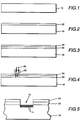
- an electrically insulating substrate 10 is shown in cross-section view. It is desired to form a conductor pattern on the upper surface of this substrate.
- This substrate may be glass, polymer materials or other relatively thermally inefficient materials.
- thermally inefficient we mean that the material is relatively slow to dissipate localized heat. In this sense, this substrate is distinct from such substrates as alumina and the high thermal conductivity metals such as copper which dissipate heat much more rapidly.
- the dividing line between thermally efficient and thermally inefficient materials is in part dependent on the energy of the laser beam used to pattern the metal.
- a first, layer of a thermally inefficient metal 22 is formed on the upper surface of the substrate 10 to provide the structure shown in Figure 2.
- This metal is preferably titanium, but may instead be chrome, nichrome, nickel, stainless steel, magnesium, manganese and so forth.
- This metal is deposited on the substrate under vacuum or other non-oxidizing conditions by any appropriate method, such as sputtering, thermal evaporation, chemical vapor deposition and so forth. We prefer to deposit this metal layer by sputtering. This layer is preferably from 500 to 1,000 ⁇ thick.
- a layer 24 of a UV absorbing metal which is preferably copper but may also be gold, is deposited on top of the layer 22 without breaking the vacuum in the deposition system to provide the structure illustrated in Figure 3.
- This copper layer may preferably be deposited to a depth in the range from 500-3,000 ⁇ . While thicker layers can be used where higher laser power is available, this thickness is adequate to the purpose, and effective with a laser power of 1-2 watts at 351-363 nm. Other wave lengths may be used with other metals having different absorption spectra.
- the substrate with its metal coating is mounted in a laser delivery system which is capable of scanning an intense UV light beam across the substrate.
- This oxidizing atmosphere may be air, air with additional oxygen added to it, pure oxygen, a chlorine containing atmosphere and so forth. We prefer to use air or air plus oxygen.
- the titanium and copper burn as they ablate with a sparkling effect similar to that of Fourth of July sparklers. This sparkling extends substantially above the surface of the metal 24.
- a beneficial side effect of this process where the substrate 10 is a polymer is that the portion of the polymer surface from which the metal is ablated becomes roughened with a surface characteristic which looks much like needles standing on their end.
- This roughened surface is a substantial advantage in a high density interconnect structure or other structure where a subsequent dielectric layer is later formed over the metal pattern and the exposed portions of the substrate 10.
- this is an adhesion promoting technique which can be applied to a polymer surface even where none of the deposited metal is to be retained on the polymer and its only function is to enable the roughening of the polymer surface during its ablation. This results in a greatly increased surface area.
- chrome used as the first or lower metal layer produces a similar sparkling and improvement in pattern definition.
- chrome used as the first or lower metal layer produces a similar sparkling and improvement in pattern definition.
- nickel, stainless steel, magnesium, manganese and similar metals which are or contain highly reactive elements will produce similar sparkling and improvement in pattern definition.
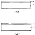
- a layer 32 of such a UV absorbing metal may be deposited directly on the substrate 10, as illustrated in Figure 6.
- the layer 32 is then patterned by use of laser ablation in the same manner as described above to selectively remove the metal 32 from the surface of the substrate 10 to produce the structure shown schematically in Figure 7.
- the resulting pattern is poorer and the substrate surface may remain conductive in the ablated regions where the substrate is a polymer.
- a thermally inefficient layer between the substrate and the ultraviolet absorbing metal in order to enable the laser ablation process to remove the UV absorbing metal.
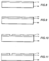
- a layer 112 of a thermally inefficient metal is vacuum deposited on a thermally conducting substrate 100 to provide the structure illustrated in Figure 8.
- This thermally inefficient metal may be titanium, chromium, stainless steel (as a laminated layer) nichrome, magnesium, manganese or other metals or mixtures or alloys of metals which are thermally inefficient and sufficiently reactive.
- the layer 112 is made thick enough to render its upper surface thermally inefficient.
- the poor thermal efficiency of the layer 112 insulates an overlying layer from the thermal efficiency of the substrate 100.
- a layer 114 of UV absorbing metal is vacuum deposited on the thermally inefficient metal 112 without breaking the vacuum in the deposition apparatus to provide the structure shown in Figure 9.
- the upper metal layer 114 protects the lower metal layer 112 from oxidation and other chemical reactions.
- the metal 114 is then ablated by a laser beam 126 as illustrated in Figure 10. This removes the UV absorbing metal 114 in the laser scan pattern and may also remove part of but not all of the thermally inefficient metal 112.
- At least the lower portion of the thermally inefficient metal remains on the substrate because for a sufficiently thin layer of the thermally inefficient metal, the underlying substrate 100 carries heat away so rapidly that the thermally inefficient layer can not be heated to an ablation temperature.
- the retained portions of that upper metal layer may be used as a mask for chemically etching of the now exposed portions of the thermally inefficient metal 112 to leave portions 120 of the substrate surface metal-free. After such etching of the exposed portions of layer 112, the structure appears as shown in Figure 11.
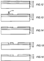
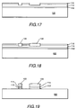
- a four layer metal structure may be formed prior to laser ablation by successfully depositing titanium, copper, titanium and copper to provide a structure of the general type shown in Figure 12.
- These layers may be ⁇ 1000 ⁇ thick titanium, ⁇ 3000 ⁇ of deposited copper on which copper is electroplated to ⁇ 3mm thick, ⁇ 500-1000 ⁇ thick titanium and ⁇ 500-3000 ⁇ thick copper, respectively.
- the upper-most copper layer 118 may then be ablated from the upper surface of the upper titanium layer 116 to leave the copper in the desired pattern for the metallization as shown in Figure 13. This ablation is generally non-reactive in that no burning or sparkling occurs and none of the titanium appears to be removed during the ablation where the titanium layer is ⁇ 500-1000 ⁇ thick.
- the now exposed portions of the underlying titanium may then be etched with an HF-based etchant to expose the thick copper layer 114 as shown in Figure 14.
- This etchant needs to be one which etches titanium without etching copper.
- a copper etch then removes the exposed portions of the lower, thick copper layer 114 and the remaining portions of the upper, thin copper layer 118 to provide the structure shown in Figure 15.
- a final titanium etch removes the now exposed portions of the lower titanium layer 112 and the portions of the upper titanium layer 116 which protected the copper of the conductor runs during the etching of the thick copper layer 114. This results in the structure shown in Figure 16
- copper layer 114 may be left with a thickness of ⁇ 6000 ⁇ or so and the layers 116 and 118 deposited thereon.
- the process then follows that described above through the etching of the upper titanium layer 116.
- the retained portions of the upper copper layer 118 are removed from the surface of the titanium by a quick copper etch in ferric chloride which leaves the layer 114 of copper ⁇ 3000 ⁇ thick as shown in Figure 17.
- Titanium forms titanium oxide when exposed to air.
- the surface of the upper titanium layer 116 is coated with titanium oxide.
- the resulting titanium oxide layer is sufficiently electrically insulating to prevent electroplating on the titanium, that is, the titanium oxide coated titanium acts as a resist for electroplating.
- this structure may then be electroplated in a copper, gold, chrome or nickel electroplating bath to produce plated conductors having the pattern of the exposed copper 114 without depositing the copper gold, chrome or nickel 122 on the titanium portion of the structure as shown in Figure 18.
- This provides an effective method of forming gold, chrome or nickel plating on copper without the problems of photoresist lifting which have been experienced in the prior art.
- the surface titanium layer may be removed in a HF-based etchant, the portions of the lower copper layer 114 which are not protected by plated metal 122 may be removed in a ferric chloride etchant and the then unprotected portions of the lower titanium layer may be removed in a HF-based etchant.
- the substrate 200 may be a single layer of insulating material or may be a multilayer printed circuit structure (including high density interconnect structures) having an insulating upper surface on which the two portions 210 and 212 of an open trace are disposed with an unintended gap 214 therebetween.
- a first layer 222 of a thermally inefficient, reactive metal such as titanium is deposited over the entire upper surface of the substrate 200 and any conductors thereon.
- a second layer 224 of a UV absorbing metal such as copper is uniformly deposited over the upper surface.
- the entire upper surface of the substrate 200 is conductive.
- the deposited metals are then laser reactive ablated from those portions of the upper surface of the substrate 200 where conductors are not desired, but without ablating the portions of the deposited metals which bridge the gap 214 between the conductors 210 and 212.
- the retained portion of the deposited metals in the vicinity of the gap between the conductors 210 and 212 serve as a bridging conductor to close the gap, thereby repairing the structure as shown in Figure 22.
- This same technique can also be used to provide temporary connections for programming during testing or for other purposes. Such temporary connections can then be removed by etching or by further laser ablation.
- a resistor 310 is disposed on a substrate 300.
- a two layer metallization 320 is disposed on top of the resistor material as its contacts. These contacts can be initially patterned by photomasking and etching. These contacts are then laser ablated to increase the length of the current path through the resistor material between the two contacts to thereby increase the resistance exhibited by the resistor. Alternatively, all of the patterning of these contacts can be done by laser ablation.
Landscapes
- Engineering & Computer Science (AREA)
- Manufacturing & Machinery (AREA)
- Microelectronics & Electronic Packaging (AREA)
- Physics & Mathematics (AREA)
- Optics & Photonics (AREA)
- Plasma & Fusion (AREA)
- Metallurgy (AREA)
- Mechanical Engineering (AREA)
- Manufacturing Of Printed Wiring (AREA)
- Parts Printed On Printed Circuit Boards (AREA)
- Apparatuses And Processes For Manufacturing Resistors (AREA)
- Manufacturing Of Printed Circuit Boards (AREA)
- Laser Beam Processing (AREA)
Applications Claiming Priority (2)
| Application Number | Priority Date | Filing Date | Title |
|---|---|---|---|
| US597255 | 1990-10-12 | ||
| US07/597,255 US5104480A (en) | 1990-10-12 | 1990-10-12 | Direct patterning of metals over a thermally inefficient surface using a laser |
Publications (3)
| Publication Number | Publication Date |
|---|---|
| EP0480703A2 true EP0480703A2 (fr) | 1992-04-15 |
| EP0480703A3 EP0480703A3 (en) | 1992-06-03 |
| EP0480703B1 EP0480703B1 (fr) | 1997-03-26 |
Family
ID=24390748
Family Applications (1)
| Application Number | Title | Priority Date | Filing Date |
|---|---|---|---|
| EP91309278A Expired - Lifetime EP0480703B1 (fr) | 1990-10-12 | 1991-10-09 | La formation de configurations de métal sur un substrat |
Country Status (4)
| Country | Link |
|---|---|
| US (1) | US5104480A (fr) |
| EP (1) | EP0480703B1 (fr) |
| JP (1) | JP3338465B2 (fr) |
| DE (1) | DE69125333T2 (fr) |
Cited By (20)
| Publication number | Priority date | Publication date | Assignee | Title |
|---|---|---|---|---|
| EP0971405A3 (fr) * | 1994-09-23 | 2000-05-10 | Siemens S.A. | Procédé pour la fabrication d'un substrat por un "stud grid array" en polymère |
| WO2000077883A1 (fr) * | 1999-06-15 | 2000-12-21 | Cts Corp. | Procede ablatif de formation de filtres rf de blocs de ceramique |
| FR2795907A1 (fr) * | 1999-07-01 | 2001-01-05 | Gemplus Card Int | Procede pour la fabrication et le test de micromodules electroniques, notamment pour cartes a puce |
| EP1047552A4 (fr) * | 1998-01-14 | 2001-04-04 | Prec Coatings Inc | Support d'imagerie a ecriture directe |
| WO2001025775A1 (fr) * | 1999-10-04 | 2001-04-12 | Roche Diagnostics Corporation | Caracteristiques definies au laser pour stratifies et electrodes a motifs |
| WO2000057468A3 (fr) * | 1999-03-24 | 2001-05-31 | Infineon Technologies Ag | Circuit electrique et procede permettant de le produire |
| US6518088B1 (en) | 1994-09-23 | 2003-02-11 | Siemens N.V. And Interuniversitair Micro-Electronica Centrum Vzw | Polymer stud grid array |
| US6559735B1 (en) | 2000-10-31 | 2003-05-06 | Cts Corporation | Duplexer filter with an alternative signal path |
| US6571468B1 (en) | 2001-02-26 | 2003-06-03 | Saturn Electronics & Engineering, Inc. | Traceless flip chip assembly and method |
| US6822332B2 (en) | 2002-09-23 | 2004-11-23 | International Business Machines Corporation | Fine line circuitization |
| US6866758B2 (en) | 2002-03-21 | 2005-03-15 | Roche Diagnostics Corporation | Biosensor |
| US6911621B2 (en) | 2000-11-01 | 2005-06-28 | Roche Diagnostics Corporation | Biosensor |
| US7073246B2 (en) | 1999-10-04 | 2006-07-11 | Roche Diagnostics Operations, Inc. | Method of making a biosensor |
| WO2006136319A1 (fr) * | 2005-06-21 | 2006-12-28 | Hansgrohe Ag | Procede pour produire des structures superficielles decoratives |
| EP1742290A1 (fr) * | 2005-07-04 | 2007-01-10 | Samsung Electronics Co., Ltd. | Antenne integrée pour un dispositif portable et procédé de fabrication de celui-ci |
| US7287318B2 (en) | 2000-10-06 | 2007-10-30 | Roche Diagnostics Operations, Inc. | Biosensor |
| US8287703B2 (en) | 1999-10-04 | 2012-10-16 | Roche Diagnostics Operations, Inc. | Biosensor and method of making |
| EP2940528A1 (fr) * | 2014-04-30 | 2015-11-04 | Wistron Neweb Corporation | Procédé de fabrication de structure de substrat et structure de substrat fabriqué à l'aide de ce procédé |
| US10369565B2 (en) | 2014-12-31 | 2019-08-06 | Abbott Laboratories | Digital microfluidic dilution apparatus, systems, and related methods |
| US10913064B2 (en) | 2014-04-16 | 2021-02-09 | Abbott Laboratories | Droplet actuator fabrication apparatus, systems, and related methods |
Families Citing this family (45)
| Publication number | Priority date | Publication date | Assignee | Title |
|---|---|---|---|---|
| GB9221099D0 (en) * | 1992-10-07 | 1992-11-18 | Ecossensors Ltd | Improvements in and relating to gas permeable membranes for amperometric gas electrodes |
| JP3400067B2 (ja) * | 1994-03-16 | 2003-04-28 | 富士通株式会社 | 印刷配線板の導体切断方法及び装置 |
| US5505320A (en) * | 1994-11-22 | 1996-04-09 | International Business Machines Corporation | Method employing laser ablating for providing a pattern on a substrate |
| US5567329A (en) * | 1995-01-27 | 1996-10-22 | Martin Marietta Corporation | Method and system for fabricating a multilayer laminate for a printed wiring board, and a printed wiring board formed thereby |
| US5821505A (en) * | 1997-04-04 | 1998-10-13 | Unisys Corporation | Temperature control system for an electronic device which achieves a quick response by interposing a heater between the device and a heat sink |
| EP0877417A1 (fr) * | 1997-05-09 | 1998-11-11 | Lucent Technologies Inc. | Procédé de fabrication d'électrodes et d'autres structures électroconductrices |
| US6141870A (en) | 1997-08-04 | 2000-11-07 | Peter K. Trzyna | Method for making electrical device |
| US6261941B1 (en) * | 1998-02-12 | 2001-07-17 | Georgia Tech Research Corp. | Method for manufacturing a multilayer wiring substrate |
| US6388230B1 (en) * | 1999-10-13 | 2002-05-14 | Morton International, Inc. | Laser imaging of thin layer electronic circuitry material |
| US6819349B2 (en) * | 2000-11-14 | 2004-11-16 | Toto Ltd. | Mark forming method and product using the same method |
| WO2002060633A1 (fr) * | 2001-02-01 | 2002-08-08 | Electro Scientific Industries, Inc. | Ajustage d'une resistance au moyen d'une tache laser uniforme faiblement dimensionnee emise par un laser ultraviolet a semi-conducteur |
| US6534743B2 (en) * | 2001-02-01 | 2003-03-18 | Electro Scientific Industries, Inc. | Resistor trimming with small uniform spot from solid-state UV laser |
| DE10112023A1 (de) * | 2001-03-07 | 2002-10-02 | Atotech Deutschland Gmbh | Verfahren zum Bilden eines Metallmusters auf einen dielektrischen Substrat |
| US6528869B1 (en) | 2001-04-06 | 2003-03-04 | Amkor Technology, Inc. | Semiconductor package with molded substrate and recessed input/output terminals |
| US20020170897A1 (en) * | 2001-05-21 | 2002-11-21 | Hall Frank L. | Methods for preparing ball grid array substrates via use of a laser |
| US6586826B1 (en) | 2001-06-13 | 2003-07-01 | Amkor Technology, Inc. | Integrated circuit package having posts for connection to other packages and substrates |
| US6814844B2 (en) * | 2001-08-29 | 2004-11-09 | Roche Diagnostics Corporation | Biosensor with code pattern |
| US20040173894A1 (en) * | 2001-09-27 | 2004-09-09 | Amkor Technology, Inc. | Integrated circuit package including interconnection posts for multiple electrical connections |
| JP4155031B2 (ja) * | 2002-03-15 | 2008-09-24 | 株式会社豊田中央研究所 | 基材の表面改質方法及び改質された基材、並びに装置 |
| US6951995B2 (en) | 2002-03-27 | 2005-10-04 | Gsi Lumonics Corp. | Method and system for high-speed, precise micromachining an array of devices |
| US7563695B2 (en) * | 2002-03-27 | 2009-07-21 | Gsi Group Corporation | Method and system for high-speed precise laser trimming and scan lens for use therein |
| GB0224121D0 (en) * | 2002-10-16 | 2002-11-27 | Microemissive Displays Ltd | Method of patterning a functional material on to a substrate |
| US20040091588A1 (en) * | 2002-10-31 | 2004-05-13 | Xiaochun Li | Food processing apparatus and method |
| TR201810169T4 (tr) | 2003-06-20 | 2018-08-27 | Hoffmann La Roche | Dar, homojen belirteç şeritlerinin üretilmesi için yöntem ve belirteç. |
| KR100784497B1 (ko) * | 2004-10-06 | 2007-12-11 | 삼성전자주식회사 | 반도체 패키지용 필름기판 및 그 제조방법 |
| WO2006100202A1 (fr) * | 2005-03-23 | 2006-09-28 | Technische Universität Ilmenau | Procede de microstructuration laser, notamment de systemes composites |
| JP4639975B2 (ja) * | 2005-06-07 | 2011-02-23 | パナソニック電工株式会社 | 立体回路基板の製造方法 |
| US8290239B2 (en) * | 2005-10-21 | 2012-10-16 | Orbotech Ltd. | Automatic repair of electric circuits |
| US7510985B1 (en) | 2005-10-26 | 2009-03-31 | Lpkf Laser & Electronics Ag | Method to manufacture high-precision RFID straps and RFID antennas using a laser |
| US20070138153A1 (en) * | 2005-12-20 | 2007-06-21 | Redman Dean E | Wide web laser ablation |
| US8647654B2 (en) * | 2005-12-22 | 2014-02-11 | The Penn State Research Foundation | Method and systems for forming and using nanoengineered sculptured thin films |
| US20070215575A1 (en) * | 2006-03-15 | 2007-09-20 | Bo Gu | Method and system for high-speed, precise, laser-based modification of one or more electrical elements |
| US8652632B2 (en) * | 2007-04-24 | 2014-02-18 | The United States Of America, As Represented By The Secretary Of The Navy | Surface enhanced raman detection on metalized nanostructured polymer films |
| JP4706690B2 (ja) * | 2007-11-05 | 2011-06-22 | パナソニック電工株式会社 | 回路基板及びその製造方法 |
| JP5405916B2 (ja) * | 2008-06-24 | 2014-02-05 | パナソニック株式会社 | バイオセンサ、その製造方法、及びそれを備える検出システム |
| US20100294352A1 (en) * | 2009-05-20 | 2010-11-25 | Uma Srinivasan | Metal patterning for electrically conductive structures based on alloy formation |
| JP2011233872A (ja) * | 2010-04-08 | 2011-11-17 | Asahi Glass Co Ltd | 金属パターン付き基板の製造方法及び金属積層体付き基板 |
| US8593727B2 (en) | 2011-04-25 | 2013-11-26 | Vladimir G. Kozlov | Single-shot laser ablation of a metal film on a polymer membrane |
| RU2494492C1 (ru) * | 2012-06-07 | 2013-09-27 | Общество с ограниченной ответственностью "Компания РМТ" | Способ создания токопроводящих дорожек |
| US10537027B2 (en) | 2013-08-02 | 2020-01-14 | Orbotech Ltd. | Method producing a conductive path on a substrate |
| EP2887418A1 (fr) * | 2013-12-19 | 2015-06-24 | The Swatch Group Research and Development Ltd. | Pile à surface structurée non condutrice |
| US9842740B2 (en) | 2014-08-29 | 2017-12-12 | Seagate Technology Llc | Ablation for feature recovery |
| KR101810815B1 (ko) * | 2017-04-07 | 2017-12-20 | 김병삼 | 마이크로 크랙 및 레이저 타공홀을 포함하는 전파투과성 센서 커버의 제조 방법 및 이를 이용하여 제조된 전파투과성 센서 커버 |
| DE102018115205A1 (de) | 2018-06-25 | 2020-01-02 | Vishay Electronic Gmbh | Verfahren zur Herstellung einer Vielzahl von Widerstandsbaueinheiten |
| CN111343793A (zh) * | 2020-03-12 | 2020-06-26 | 电子科技大学 | 一种印制电路复合介质基板表面金属化方法 |
Family Cites Families (7)
| Publication number | Priority date | Publication date | Assignee | Title |
|---|---|---|---|---|
| US3867217A (en) * | 1973-10-29 | 1975-02-18 | Bell Telephone Labor Inc | Methods for making electronic circuits |
| DE2521543A1 (de) * | 1974-05-16 | 1975-11-27 | Crosfield Electronics Ltd | Verfahren und vorrichtung zur wiedergabe von bildern |
| US4259433A (en) * | 1976-10-22 | 1981-03-31 | Fuji Photo Film Co., Ltd. | Method for producing disk-recording plates |
| US4713518A (en) * | 1984-06-08 | 1987-12-15 | Semiconductor Energy Laboratory Co., Ltd. | Electronic device manufacturing methods |
| JPS61108195A (ja) * | 1984-11-01 | 1986-05-26 | インタ−ナショナル ビジネス マシ−ンズ コ−ポレ−ション | 基板上に電気的に連続した層を形成する方法 |
| US4786358A (en) * | 1986-08-08 | 1988-11-22 | Semiconductor Energy Laboratory Co., Ltd. | Method for forming a pattern of a film on a substrate with a laser beam |
| US4826785A (en) * | 1987-01-27 | 1989-05-02 | Inmos Corporation | Metallic fuse with optically absorptive layer |
-
1990
- 1990-10-12 US US07/597,255 patent/US5104480A/en not_active Expired - Lifetime
-
1991
- 1991-10-03 JP JP28202991A patent/JP3338465B2/ja not_active Expired - Fee Related
- 1991-10-09 DE DE69125333T patent/DE69125333T2/de not_active Expired - Fee Related
- 1991-10-09 EP EP91309278A patent/EP0480703B1/fr not_active Expired - Lifetime
Cited By (34)
| Publication number | Priority date | Publication date | Assignee | Title |
|---|---|---|---|---|
| EP0971405A3 (fr) * | 1994-09-23 | 2000-05-10 | Siemens S.A. | Procédé pour la fabrication d'un substrat por un "stud grid array" en polymère |
| US6518088B1 (en) | 1994-09-23 | 2003-02-11 | Siemens N.V. And Interuniversitair Micro-Electronica Centrum Vzw | Polymer stud grid array |
| EP1047552A4 (fr) * | 1998-01-14 | 2001-04-04 | Prec Coatings Inc | Support d'imagerie a ecriture directe |
| US6350555B1 (en) | 1998-01-14 | 2002-02-26 | Precision Coatings, Inc. | Direct write imaging medium |
| WO2000057468A3 (fr) * | 1999-03-24 | 2001-05-31 | Infineon Technologies Ag | Circuit electrique et procede permettant de le produire |
| US6834429B2 (en) | 1999-06-15 | 2004-12-28 | Cts Corporation | Ablative method for forming RF ceramic block filters |
| US6462629B1 (en) | 1999-06-15 | 2002-10-08 | Cts Corporation | Ablative RF ceramic block filters |
| WO2000077883A1 (fr) * | 1999-06-15 | 2000-12-21 | Cts Corp. | Procede ablatif de formation de filtres rf de blocs de ceramique |
| WO2001003185A1 (fr) * | 1999-07-01 | 2001-01-11 | Gemplus | Procede pour la fabrication et le test de micromodules electroniques, notamment pour cartes a puce |
| FR2795907A1 (fr) * | 1999-07-01 | 2001-01-05 | Gemplus Card Int | Procede pour la fabrication et le test de micromodules electroniques, notamment pour cartes a puce |
| WO2001025775A1 (fr) * | 1999-10-04 | 2001-04-12 | Roche Diagnostics Corporation | Caracteristiques definies au laser pour stratifies et electrodes a motifs |
| US8551308B2 (en) | 1999-10-04 | 2013-10-08 | Roche Diagnostics Operations, Inc. | Biosensor and method of making |
| US8287703B2 (en) | 1999-10-04 | 2012-10-16 | Roche Diagnostics Operations, Inc. | Biosensor and method of making |
| US6662439B1 (en) | 1999-10-04 | 2003-12-16 | Roche Diagnostics Corporation | Laser defined features for patterned laminates and electrodes |
| US7073246B2 (en) | 1999-10-04 | 2006-07-11 | Roche Diagnostics Operations, Inc. | Method of making a biosensor |
| US7287318B2 (en) | 2000-10-06 | 2007-10-30 | Roche Diagnostics Operations, Inc. | Biosensor |
| US6559735B1 (en) | 2000-10-31 | 2003-05-06 | Cts Corporation | Duplexer filter with an alternative signal path |
| US6911621B2 (en) | 2000-11-01 | 2005-06-28 | Roche Diagnostics Corporation | Biosensor |
| WO2002071471A3 (fr) * | 2001-02-26 | 2003-10-30 | Saturn Electronics & Eng Inc | Assemblage puce a bosse sans trace et procede correspondant |
| US6846701B2 (en) | 2001-02-26 | 2005-01-25 | Saturn Electronics & Engineering, Inc. | Traceless flip chip assembly and method |
| US6571468B1 (en) | 2001-02-26 | 2003-06-03 | Saturn Electronics & Engineering, Inc. | Traceless flip chip assembly and method |
| US6866758B2 (en) | 2002-03-21 | 2005-03-15 | Roche Diagnostics Corporation | Biosensor |
| US7185428B2 (en) | 2002-09-23 | 2007-03-06 | International Business Machines Corporation | Method of making a circuitized substrate |
| US6822332B2 (en) | 2002-09-23 | 2004-11-23 | International Business Machines Corporation | Fine line circuitization |
| US7325299B2 (en) | 2002-09-23 | 2008-02-05 | International Business Machines Corporation | Method of making a circuitized substrate |
| US7596862B2 (en) | 2002-09-23 | 2009-10-06 | International Business Machines Corporation | Method of making a circuitized substrate |
| JP2007524076A (ja) * | 2003-06-20 | 2007-08-23 | エフ ホフマン−ラ ロッシュ アクチェン ゲゼルシャフト | バイオセンサーおよび作製方法 |
| WO2006136319A1 (fr) * | 2005-06-21 | 2006-12-28 | Hansgrohe Ag | Procede pour produire des structures superficielles decoratives |
| EP1742290A1 (fr) * | 2005-07-04 | 2007-01-10 | Samsung Electronics Co., Ltd. | Antenne integrée pour un dispositif portable et procédé de fabrication de celui-ci |
| US10913064B2 (en) | 2014-04-16 | 2021-02-09 | Abbott Laboratories | Droplet actuator fabrication apparatus, systems, and related methods |
| US12201980B2 (en) | 2014-04-16 | 2025-01-21 | Abbott Laboratories | Droplet actuator fabrication apparatus, systems, and related methods |
| EP2940528A1 (fr) * | 2014-04-30 | 2015-11-04 | Wistron Neweb Corporation | Procédé de fabrication de structure de substrat et structure de substrat fabriqué à l'aide de ce procédé |
| US10369565B2 (en) | 2014-12-31 | 2019-08-06 | Abbott Laboratories | Digital microfluidic dilution apparatus, systems, and related methods |
| US11213817B2 (en) | 2014-12-31 | 2022-01-04 | Abbott Laboratories | Digital microfluidic dilution apparatus, systems, and related methods |
Also Published As
| Publication number | Publication date |
|---|---|
| JP3338465B2 (ja) | 2002-10-28 |
| EP0480703A3 (en) | 1992-06-03 |
| US5104480A (en) | 1992-04-14 |
| DE69125333T2 (de) | 1997-10-02 |
| DE69125333D1 (de) | 1997-04-30 |
| EP0480703B1 (fr) | 1997-03-26 |
| JPH04280494A (ja) | 1992-10-06 |
Similar Documents
| Publication | Publication Date | Title |
|---|---|---|
| US5104480A (en) | Direct patterning of metals over a thermally inefficient surface using a laser | |
| JP3587884B2 (ja) | 多層回路基板の製造方法 | |
| US6119335A (en) | Method for manufacturing multi-layer printed circuit board | |
| JP3361556B2 (ja) | 回路配線パタ−ンの形成法 | |
| EP0843955B1 (fr) | Procede permettant de former des contacts metalliques saillants dans des circuits electriques | |
| US5107586A (en) | Method for interconnecting a stack of integrated circuits at a very high density | |
| US4258468A (en) | Forming vias through multilayer circuit boards | |
| US4704304A (en) | Method for repair of opens in thin film lines on a substrate | |
| EP0366259B1 (fr) | Procédé pour interconnecter des circuits électriques à film mince | |
| EP0206337B1 (fr) | Substrat pour des connexions multicouches comprenant des plages de câblage de rechange | |
| EP0611121A2 (fr) | Procédé pour faire une configuration dans des diélectriques et structures en résultant | |
| EP0450381B1 (fr) | Structure d'interconnexion multi-couche | |
| US4983250A (en) | Method of laser patterning an electrical interconnect | |
| EP0660382A2 (fr) | Circuit hybride et procédé de fabrication | |
| JPH10214920A (ja) | 改良型ポリテトラフルオロエチレン薄膜チップ・キャリア | |
| EP0436282A2 (fr) | Procédé de métallisation sélective | |
| US5230965A (en) | High density interconnect with electroplated conductors | |
| JPH0734508B2 (ja) | 多層配線板 | |
| WO1989002697A1 (fr) | Procede de metallisation induit par la dissociation d'une ceramique a base de nitrure d'aluminium | |
| US5550325A (en) | Printed-circuit board including circuit pattern having location to be cut if necessary | |
| JPH07202424A (ja) | 多層配線基板の製造方法 | |
| JP3154964B2 (ja) | プリント基板およびそのレーザ穴あけ方法 | |
| GB2307351A (en) | Printed circuit boards and their manufacture | |
| JP3136682B2 (ja) | 多層配線基板の製造方法 | |
| Scholz et al. | High via density thin metal-core PCB using electro-coated dielectric |
Legal Events
| Date | Code | Title | Description |
|---|---|---|---|
| PUAI | Public reference made under article 153(3) epc to a published international application that has entered the european phase |
Free format text: ORIGINAL CODE: 0009012 |
|
| AK | Designated contracting states |
Kind code of ref document: A2 Designated state(s): DE FR GB IT |
|
| PUAL | Search report despatched |
Free format text: ORIGINAL CODE: 0009013 |
|
| AK | Designated contracting states |
Kind code of ref document: A3 Designated state(s): DE FR GB IT |
|
| 17P | Request for examination filed |
Effective date: 19921123 |
|
| 17Q | First examination report despatched |
Effective date: 19941005 |
|
| GRAG | Despatch of communication of intention to grant |
Free format text: ORIGINAL CODE: EPIDOS AGRA |
|
| GRAH | Despatch of communication of intention to grant a patent |
Free format text: ORIGINAL CODE: EPIDOS IGRA |
|
| GRAH | Despatch of communication of intention to grant a patent |
Free format text: ORIGINAL CODE: EPIDOS IGRA |
|
| GRAA | (expected) grant |
Free format text: ORIGINAL CODE: 0009210 |
|
| AK | Designated contracting states |
Kind code of ref document: B1 Designated state(s): DE FR GB IT |
|
| ET | Fr: translation filed | ||
| REF | Corresponds to: |
Ref document number: 69125333 Country of ref document: DE Date of ref document: 19970430 |
|
| PLBE | No opposition filed within time limit |
Free format text: ORIGINAL CODE: 0009261 |
|
| STAA | Information on the status of an ep patent application or granted ep patent |
Free format text: STATUS: NO OPPOSITION FILED WITHIN TIME LIMIT |
|
| 26N | No opposition filed | ||
| REG | Reference to a national code |
Ref country code: FR Ref legal event code: TP |
|
| PGFP | Annual fee paid to national office [announced via postgrant information from national office to epo] |
Ref country code: FR Payment date: 20010920 Year of fee payment: 11 Ref country code: DE Payment date: 20010920 Year of fee payment: 11 |
|
| PGFP | Annual fee paid to national office [announced via postgrant information from national office to epo] |
Ref country code: GB Payment date: 20010921 Year of fee payment: 11 |
|
| REG | Reference to a national code |
Ref country code: GB Ref legal event code: 732E |
|
| REG | Reference to a national code |
Ref country code: GB Ref legal event code: IF02 |
|
| PG25 | Lapsed in a contracting state [announced via postgrant information from national office to epo] |
Ref country code: GB Free format text: LAPSE BECAUSE OF NON-PAYMENT OF DUE FEES Effective date: 20021009 |
|
| PG25 | Lapsed in a contracting state [announced via postgrant information from national office to epo] |
Ref country code: DE Free format text: LAPSE BECAUSE OF NON-PAYMENT OF DUE FEES Effective date: 20030501 |
|
| GBPC | Gb: european patent ceased through non-payment of renewal fee |
Effective date: 20021009 |
|
| PG25 | Lapsed in a contracting state [announced via postgrant information from national office to epo] |
Ref country code: FR Free format text: LAPSE BECAUSE OF NON-PAYMENT OF DUE FEES Effective date: 20030630 |
|
| REG | Reference to a national code |
Ref country code: FR Ref legal event code: ST |
|
| PG25 | Lapsed in a contracting state [announced via postgrant information from national office to epo] |
Ref country code: IT Free format text: LAPSE BECAUSE OF NON-PAYMENT OF DUE FEES Effective date: 20051009 |