EP0480775A2 - Bildsensor und Verfahren zur Bildsensorprüfung - Google Patents
Bildsensor und Verfahren zur Bildsensorprüfung Download PDFInfo
- Publication number
- EP0480775A2 EP0480775A2 EP91309425A EP91309425A EP0480775A2 EP 0480775 A2 EP0480775 A2 EP 0480775A2 EP 91309425 A EP91309425 A EP 91309425A EP 91309425 A EP91309425 A EP 91309425A EP 0480775 A2 EP0480775 A2 EP 0480775A2
- Authority
- EP
- European Patent Office
- Prior art keywords
- photo
- image sensor
- image sensors
- sensing elements
- diffusion layer
- Prior art date
- Legal status (The legal status is an assumption and is not a legal conclusion. Google has not performed a legal analysis and makes no representation as to the accuracy of the status listed.)
- Pending
Links
Images


Classifications
-
- H—ELECTRICITY
- H04—ELECTRIC COMMUNICATION TECHNIQUE
- H04N—PICTORIAL COMMUNICATION, e.g. TELEVISION
- H04N1/00—Scanning, transmission or reproduction of documents or the like, e.g. facsimile transmission; Details thereof
- H04N1/024—Details of scanning heads ; Means for illuminating the original
- H04N1/028—Details of scanning heads ; Means for illuminating the original for picture information pick-up
- H04N1/03—Details of scanning heads ; Means for illuminating the original for picture information pick-up with photodetectors arranged in a substantially linear array
- H04N1/0308—Details of scanning heads ; Means for illuminating the original for picture information pick-up with photodetectors arranged in a substantially linear array characterised by the design of the photodetectors, e.g. shape
-
- H—ELECTRICITY
- H04—ELECTRIC COMMUNICATION TECHNIQUE
- H04N—PICTORIAL COMMUNICATION, e.g. TELEVISION
- H04N1/00—Scanning, transmission or reproduction of documents or the like, e.g. facsimile transmission; Details thereof
- H04N1/024—Details of scanning heads ; Means for illuminating the original
- H04N1/028—Details of scanning heads ; Means for illuminating the original for picture information pick-up
- H04N1/03—Details of scanning heads ; Means for illuminating the original for picture information pick-up with photodetectors arranged in a substantially linear array
-
- H—ELECTRICITY
- H04—ELECTRIC COMMUNICATION TECHNIQUE
- H04N—PICTORIAL COMMUNICATION, e.g. TELEVISION
- H04N1/00—Scanning, transmission or reproduction of documents or the like, e.g. facsimile transmission; Details thereof
- H04N1/04—Scanning arrangements, i.e. arrangements for the displacement of active reading or reproducing elements relative to the original or reproducing medium, or vice versa
- H04N1/19—Scanning arrangements, i.e. arrangements for the displacement of active reading or reproducing elements relative to the original or reproducing medium, or vice versa using multi-element arrays
- H04N1/191—Scanning arrangements, i.e. arrangements for the displacement of active reading or reproducing elements relative to the original or reproducing medium, or vice versa using multi-element arrays the array comprising a one-dimensional [1D] array
- H04N1/192—Simultaneously or substantially simultaneously scanning picture elements on one main scanning line
- H04N1/193—Simultaneously or substantially simultaneously scanning picture elements on one main scanning line using electrically scanned linear arrays, e.g. linear CCD arrays
- H04N1/1934—Combination of arrays
-
- H—ELECTRICITY
- H10—SEMICONDUCTOR DEVICES; ELECTRIC SOLID-STATE DEVICES NOT OTHERWISE PROVIDED FOR
- H10F—INORGANIC SEMICONDUCTOR DEVICES SENSITIVE TO INFRARED RADIATION, LIGHT, ELECTROMAGNETIC RADIATION OF SHORTER WAVELENGTH OR CORPUSCULAR RADIATION
- H10F39/00—Integrated devices, or assemblies of multiple devices, comprising at least one element covered by group H10F30/00, e.g. radiation detectors comprising photodiode arrays
- H10F39/011—Manufacture or treatment of image sensors covered by group H10F39/12
- H10F39/028—Manufacture or treatment of image sensors covered by group H10F39/12 performed after manufacture of the image sensors, e.g. annealing, gettering of impurities, short-circuit elimination or recrystallisation
-
- H—ELECTRICITY
- H10—SEMICONDUCTOR DEVICES; ELECTRIC SOLID-STATE DEVICES NOT OTHERWISE PROVIDED FOR
- H10F—INORGANIC SEMICONDUCTOR DEVICES SENSITIVE TO INFRARED RADIATION, LIGHT, ELECTROMAGNETIC RADIATION OF SHORTER WAVELENGTH OR CORPUSCULAR RADIATION
- H10F39/00—Integrated devices, or assemblies of multiple devices, comprising at least one element covered by group H10F30/00, e.g. radiation detectors comprising photodiode arrays
- H10F39/10—Integrated devices
- H10F39/12—Image sensors
Definitions
- the present invention relates to image sensors and in particular, but not exclusively, to linear image sensors which are installed in facsimile apparatus, image scanners, digital copiers etc., for reading text and diagrams.
- the present invention also relates to a method of inspecting image sensors which are formed in an array on a semiconductor wafer and in particular, but not exclusively, to contact type linear image sensors which are used in image readers such as facsimile apparatus, image scanners for desk top publishing apparatus, digital copiers and bar code readers.
- Figure 2(a) is a crow section of a photo diode light receiving element, a linear array of which comprises a linear image sensor.
- the linear image sensor is formed on an n type semiconductor substrate (11) on which is disposed an n type impurity layer (12).
- Each element is formed by a p type high impurity concentration diffusion layer (14).
- Each element is surrounded by an isolation layer (16) of an n type impurity diffusion.
- An inter-insulating field (13) of silicon dioxide is deposited on the surface of the substrate so as to deactivate it. The elements are thus arranged to receive light radiation h ⁇ falling on the diffusion layers (14).
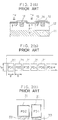
- the linear image sensor comprises photo-sensing elements (21) all of which are the same size.
- the photo-sensing element (22) has a different size from the other photosensing elements (21).
- the photo-sensing elements (22) which are at the end positions of the image sensor have a different shape to the other photo-sensing elements (21) due to the way in which the image sensor is manufactured. That is to say, a plurality of image sensors are manufactured together on one wafer and are connected linearly to form one long linear sensor. The linear image sensors are then defined by a dicing process which separates each of the image sensors. Often, the end position of the image sensor is partially destroyed by the dicing process and the width of the partially destroyed portion may vary from a few ⁇ m to 30 ⁇ m. Damage to the end photosensing element leads to instability of the p-n diffusion junction.
- each of the photo-sensing elements (31, 32) are coupled to an electrode (33).
- Each of the photo-sensing elements are receptive to light radiation h ⁇ to store photo-excited carriers.
- Regionally generated photo-sensing carriers in the photo-sensing elements (21,22) are the same in number. However, the distance travelled for the photo-excited carriers stored in the photo-sensing element (22, 32) is longer than for those photo-excited carriers stored in the internal photo-sensing elements (21, 31). Consequently, the field intensity of photo-sensing elements (21, 22) is different. The consequence of this leads to a difference in reading time between photo-sensing elements (21, 22) which has been found to cause a problem.
- the photo-sensing elements are preferably made so as to have the same size and arranged equi-distantly from each other.
- the surface areas of the elements must be made the same and arranged equi-distant from each other. But this has meant in the past that there is a lack of photo response uniformity from linear image sensors.
- FIG. 7 illustrates part of a semiconductor wafer having a plurality of linear image sensors separated by boundaries (44) and each of the image sensors comprises a linear array of photo sensitive elements (42). Prior to isolating individual image sensors (50), the photo electric conversion characteristics of each of the image sensors are inspected by irradiating the surface of the semiconductor wafer.
- Figure 8 illustrates a sectional view of a number of image sensors (50) being inspected by an inspection needle (51) which irradiates the surface of the semiconductor wafer.
- the boundaries (44) are also irradiated.
- Photo-sensing carriers(62) are thus generated in the boundaries (44) and may be able to penetrate a diffusion layer (43) forming the photo-sensing element (42) which is part of the image sensor (50) being inspected.
- the detected photo-electric conversion efficiency of the image sensor (50) is thus increased.
- This detected photo-electric conversion efficiency is particularly not comparable with the actual photo-electric conversion efficiency when the inspected linear image sensors are used in the form of multi chip and contact type linear image sensors which are eventually separated to form individual linear image sensors.
- the actual photo-electric conversion characteristics of the image sensor are significantly less than the detected photo-electric conversion efficiency because photo-sensing carriers (45) are only generated by light being irradiated through the photo-sensing lens (42).
- the actual photo-conversion efficiency of an image sensor can be 20 to 60 per cent lower than the detected photo-electric conversion efficiency when the image sensor is inspected whilst in contact with other linear image sensors.
- One aim of the present invention is therefore to provide an image sensor which has improved photo response uniformity.
- a further aim of the present invention is to provide a method of inspecting image sensors to improve the accuracy of obtaining the photo-electric efficiency of an image sensor.
- an image sensor comprising: a semiconductor substrate of a first conductivity type; two or more photo-sensing elements disposed on said substrate each comprising an impurity diffusion layer having a second conductivity type; characterised by each impurity diffusion layer having the same shape and size; and by a layer which is opaque to radiation disposed on said photo-sensing elements having two or more windows each of which overlaps with a respective photo-sensing element such that each window exposes the same surface area of impurity diffusion layer thereby improving photo response uniformity.
- the uniform shape of the diffusion layers and the windows in the opaque layer provide a uniform surface area for the photo-sensing element exposed to the radiation irrespective of whether the photo-sensing element is at the end position of an image sensor and consequently the above problem is thereby obviated.
- the opaque layer is a metallic thin film.
- the number of photo excited carriers of each of the photo-sensing elements is thus approximately equal.
- the insulation capacity between the impurity diffusion layers and the opaque metallic thin film layer is approximately equal. This leads to the output impedance and common-emitter current gain hfe from each of the photo-sensing elements when converting the light received to an output signal to be approximately uniform.
- a method of inspecting an image sensor formed on a surface of a semiconductor wafer characterised by: cutting grooves at the boundaries between the image sensor under inspection and adjacent image sensors formed on the surface of the semiconductor wafer, and irradiating the semiconductor wafer to determine the photo-electric conversion efficiency of the image sensor under inspection.
- a method of manufacturing image sensors comprising; forming two or more image sensors on a semiconductor wafer; characterised by cutting grooves at the boundaries between each of the image sensors; irradiating the semiconductor wafer to determine the photo electric conversion efficiency of one of more the image sensors; and cutting the wafer at the boundaries so as to separate the image sensors
- an image sensor head comprising; a base plate; one or more semiconductor substrates of a first conductivity type on each of which is disposed two or more photo-sensing elements arrayed linearly in a main scanning direction, each photo-sensing element comprising an impurity diffusion layer having a second conductivity type; characterised by a layer which is a opaque to radiation disposed on each of said photosensing elements having two or more windows, each of which overlaps with a respective photo-sensing element and each of which has the same shape thereby improving the photo response uniformity of the image sensor head.
- an image sensor comprises a number of photo-sensing elements arranged on the surface of a semiconductor substrate (1).
- the semiconductor substrate (1) comprises silicon and is of an n type conductivity.
- the photo-sensing elements are formed by an impurity diffusion layer (3) which has a p type conductivity.
- This impurity diffusion layer (3) may be formed from high density Boron B or Indium In.
- the layer (3) effectively stores the positive charge left by the photo excited carriers generated by the substrate (10) on radiation h ⁇ .
- Each of the photo-sensing elements is surrounded by an isolation layer (2).
- the isolation layer (2) is of an n type conductivity and may be formed from doping with phosphorus P, arsenic As or antimony Sb.
- the surface of the substrate (1) is then covered by an inter-insulating film (4) over and above the aforementioned layer.
- This inter-insulating film (4) needs to be transparent and usually comprising silicon dioxide.
- the film (4) may be formed by thermal oxidation or chemical vapour deposition and so on.
- a film (5) is then disposed on the inter-insulating film (4) which is opaque to radiation.
- the film (5) there are formed one or more windows each of which correspond to a respective photo sensing element (3). Consequently the film (5) shades the semiconductor substrate and determines the areas of the semiconductor substrate which may be irradiated.
- This shading film (5) may be formed from a metallic film comprising alluminium Al.
- the shading film (5) may be formed by depositing the metal through sputtering or vaccum evaporation which is then etched and patterned.
- a further layer is then deposited on the semicondutor substrate.
- This layer comprises of a passivation film (6) consisting of transparent phosphrous silicate glass PSG or silicon nitride Si3N4.
- the passivation film (6) protects the semicondutor substrate (1) from ion impurities or moisture.
- the photo-sensing elements (3) are arranged linearly and become the detecting portion of a linear image sensor.
- PD1, PD2. etc. are windows in the non transmittable metallic thin film (5).
- the photo sensing elements all have the same shape and surface area.
- the non transmittable metallic thin film (5) overlaps the diffusion layer (3) of each photo-sensing element.
- the areas of the diffusion layer of the internal photo-sensing elements which are covered by the non transmittable metallic thin film (5) are referenced S or1 S or2 . These overlapped portions S or1 S or2 generate an insulative capacity COR.
- Those photo-sensing elements positioned at the end portions of the image sensor have an overlap portion S E .
- the overlap portions are different in shape they are equal in area and consequently the insulation capacity CE of the overlap portions of the photo-sensitive elements at the end portions of the image sensor are equal to the insulation capacity COR of the overlap portions of the internal photo-sensing elements.
- the output impedance and common emmitter current gain hfe for the end positioned photo-sensing elements and other photosensing elements when reading text are approximately uniform. The reading time is also approximately the same. This leads to enhanced photo response uniformity.
- the photo-sensing elements comprise photo transistors
- the common emitter current gain hfe becomes uniform by making each form of impurity diffusion layer equal.
- the photo response uniformity of the photo transistor type linear image sensors is then more uniform.
- the photo response uniformity from photo transistor type image sensors is more than for photo diode type image sensors.
- the preferred embodiment of the present invention thus enables the generated photo excited carriers which are stored to be the same in each photo sensing element.
- each photo sensing element reads at the same rate. This thus improves the photo response conversion efficiency. Consequently, in spite of the photo sensing element positioned at the end portions being of a different shape due to the limitations in the mounting operation, the photo response from these photo sensing elements do not differ from the other photo sensing elements. Poor quality of images from these end positioned photo sensing elements is thus obviated.
- the windows can be positioned equi-distantly along the image sensor yet allowing the photo sensing element at the end position to be disposed closer to its adjacent photo sensing element.
- the damage caused by cutting the semiconductor substrate can be minimised since the photo sensing elements will not be positioned close to the edge of the image sensor.
- This also improves the photo response conversion efficiency. There will be some generated photo excited carriers that will be destroyed in the dicing process but of a relatively small number and which will not effect greatly the photo response uniformity achieved by the preferred embodiment.
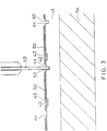
- FIG 3 there is shown a cross section of the semiconductor wafer (41) placed on a dicing saw stage (54).
- the semiconductor wafer (41) has a number of image sensors (50 ) with a boundary (44) between adjacent image sensors.
- a dicing saw blade (53) cuts grooves into the semicondutor wafer (41) at the boundaries (44). It has been found by the inventors that the optimum depth for cutting the grooves is in the order of 10 ⁇ m or deeper. This is because light is absorbed by the semiconductor wafer within a depth of 10 ⁇ m.
- the distance between the grooves (52) and the diffusion layer (43) on the linear image sensor (50) is preferably at least 5 ⁇ m. These dimensions are chosen to minimise photo sensing carriers stored in the diffusion layers (43) from translocating to other image sensors due to the distortion on the surface of the semicondutor wafer (41).
- Figure 4 illustrates a semiconductor wafer having grooves (52) cut into each boundary (44) between the linear image sensors (50).
- Each of the linear image sensors are then inspected using a solid state imaging device tester which is usually an inspection needle (51).
- the inspection needle (51) probes each of the linear image sensors (50) to test if it functions normally.
- the inspection needle (51) probes each of the linear image sensors (50) to test if it functions normally.
- the photo sensing carriers (62) generated by radiation in the boundary region (44) are caught or recombined in the region of deformed lattice of distorted region created by the grooves (52).
- those photo sensing carriers (61) generated around the linear image sensors (50) being inspected are diffused or recombined remotely and at a large depth from the surface of the semiconductor wafer (41) or are diffused to the grooves (52) then recombined. Consequently, most of the photo sensing carriers stored in the diffusion layer (43) are photo sensing carriers (45) generating by the irradiation of light h ⁇ through the photo sensing window (42) of the particular linear image sensor (50) being inspected.
- This method of inspecting a linear image sensor enables a more accurate photo electric conversion characteristic to be assessed when the linear image sensors are still connnected together on the semiconductor wafer prior to being separated. Although the method is simple, it is highly effective.
- the image sensor head (80) comprises a base plate (70) with a plurality of image sensors (10) mounted on the base plate (70) in a linear arrangement with respect to the main scanning direction. Adjacent image sensors (10) are disposed closely with a gap of less than several 10 ⁇ m.
- Such an image sensor head of the contact type have a uniform output performance which has not been known hitherto yet with an extremely simple construction.
- the grooves cut between adjacent image sensors may be formed by a scraper or a laser.
- a plasma etcher may be used to form the grooves during the ordinary semiconductor fabrication process.
Landscapes
- Engineering & Computer Science (AREA)
- Multimedia (AREA)
- Signal Processing (AREA)
- Solid State Image Pick-Up Elements (AREA)
Applications Claiming Priority (4)
| Application Number | Priority Date | Filing Date | Title |
|---|---|---|---|
| JP2273527A JP3047114B2 (ja) | 1990-10-12 | 1990-10-12 | リニアイメージセンサー |
| JP273527/90 | 1990-10-12 | ||
| JP2321839A JP2714998B2 (ja) | 1990-11-26 | 1990-11-26 | リニアイメージセンサーの検査方法 |
| JP321839/90 | 1990-11-26 |
Publications (2)
| Publication Number | Publication Date |
|---|---|
| EP0480775A2 true EP0480775A2 (de) | 1992-04-15 |
| EP0480775A3 EP0480775A3 (en) | 1992-07-15 |
Family
ID=26550699
Family Applications (1)
| Application Number | Title | Priority Date | Filing Date |
|---|---|---|---|
| EP19910309425 Pending EP0480775A3 (en) | 1990-10-12 | 1991-10-14 | An image sensor and a method of inspecting image sensors |
Country Status (2)
| Country | Link |
|---|---|
| US (2) | US5329149A (de) |
| EP (1) | EP0480775A3 (de) |
Cited By (2)
| Publication number | Priority date | Publication date | Assignee | Title |
|---|---|---|---|---|
| EP0657938A1 (de) * | 1993-12-06 | 1995-06-14 | Minnesota Mining And Manufacturing Company | Festkörperstrahlungsdetektortafel mit matrixförmig angeordneten, lichtempfindlichen Detektoren, so angeordnet, dass Kanteneffekte zwischen den Elementen minimiert werden |
| CN101945259A (zh) * | 2010-09-13 | 2011-01-12 | 珠海全志科技有限公司 | 一种视频图像叠加与遮挡的装置和方法 |
Families Citing this family (12)
| Publication number | Priority date | Publication date | Assignee | Title |
|---|---|---|---|---|
| US6865000B2 (en) * | 1994-12-06 | 2005-03-08 | Canon Kabushiki Kaisha | Image reading apparatus for grouping sensors according to characteristics |
| US5659189A (en) * | 1995-06-07 | 1997-08-19 | Lsi Logic Corporation | Layout configuration for an integrated circuit gate array |
| US5552828A (en) * | 1995-08-17 | 1996-09-03 | Xerox Corporation | Geometries for photosites in a photosensitive silicon chip |
| US6407418B1 (en) * | 1998-09-16 | 2002-06-18 | Nec Corporation | Semiconductor device, method of manufacturing the same, image sensor apparatus having the same and image reader having the same |
| US6147372A (en) * | 1999-02-08 | 2000-11-14 | Taiwan Semiconductor Manufacturing Company | Layout of an image sensor for increasing photon induced current |
| US6633058B1 (en) | 1999-07-26 | 2003-10-14 | Dalsa, Inc. | Variable reticulation time delay and integrate sensor |
| US6515269B1 (en) | 2000-01-25 | 2003-02-04 | Amkor Technology, Inc. | Integrally connected image sensor packages having a window support in contact with a window and the active area |
| US6512219B1 (en) * | 2000-01-25 | 2003-01-28 | Amkor Technology, Inc. | Fabrication method for integrally connected image sensor packages having a window support in contact with the window and active area |
| JP2002050754A (ja) * | 2000-05-08 | 2002-02-15 | Canon Inc | 半導体装置とその製造方法、放射線検出装置とそれを用いた放射線検出システム |
| US6503780B1 (en) | 2000-07-05 | 2003-01-07 | Amkor Technology, Inc. | Wafer scale image sensor package fabrication method |
| TW530480B (en) * | 2001-09-27 | 2003-05-01 | Microtek Int Inc | Image sensor device and control method of scanner using the same |
| JP2006337189A (ja) * | 2005-06-02 | 2006-12-14 | Fujifilm Holdings Corp | 半導体装置の製造方法 |
Family Cites Families (27)
| Publication number | Priority date | Publication date | Assignee | Title |
|---|---|---|---|---|
| FR2100997B1 (de) * | 1970-08-04 | 1973-12-21 | Silec Semi Conducteurs | |
| US4182024A (en) * | 1977-12-15 | 1980-01-08 | National Semiconductor Corporation | Automatic control of integrated circuit trimming |
| JPS55124277A (en) * | 1979-03-19 | 1980-09-25 | Nec Corp | Semiconductor photodetector |
| JPS57157680A (en) * | 1981-03-25 | 1982-09-29 | Toshiba Corp | Line sensor for picture reading |
| JPS58171A (ja) * | 1981-06-25 | 1983-01-05 | Toshiba Corp | 固体撮像素子 |
| JPS58155757A (ja) * | 1982-03-11 | 1983-09-16 | Matsushita Electric Ind Co Ltd | 固体撮像装置 |
| JPS6042843A (ja) * | 1983-08-18 | 1985-03-07 | Rohm Co Ltd | 半導体ウェファ |
| JPS6114749A (ja) * | 1984-06-29 | 1986-01-22 | Fujitsu Ltd | 半導体装置 |
| KR900002808B1 (ko) * | 1984-07-26 | 1990-04-30 | 가부시끼 가이샤 도시바 | 화상 판독 장치 |
| JPS6149463A (ja) * | 1984-08-17 | 1986-03-11 | Matsushita Electronics Corp | 一次元イメ−ジセンサ |
| JPS61141175A (ja) * | 1984-12-14 | 1986-06-28 | Hamamatsu Photonics Kk | 半導体光検出装置 |
| JPS61292360A (ja) * | 1985-06-20 | 1986-12-23 | Toshiba Corp | 固体撮像装置 |
| JPS6212154A (ja) * | 1985-07-10 | 1987-01-21 | Hitachi Ltd | 固体撮像装置 |
| EP0246481B1 (de) * | 1986-05-13 | 1990-12-27 | Heimann GmbH | Kontaktbildsensorzeile |
| JPS62269357A (ja) * | 1986-05-19 | 1987-11-21 | Sony Corp | 固体撮像装置 |
| JPH0828496B2 (ja) * | 1987-03-31 | 1996-03-21 | 株式会社東芝 | 固体撮像装置 |
| JPH0666452B2 (ja) * | 1987-09-04 | 1994-08-24 | 株式会社東芝 | 固体撮像装置の製造方法 |
| US5028970A (en) * | 1987-10-14 | 1991-07-02 | Fuji Photo Film Co., Ltd. | Image sensor |
| JPH01205566A (ja) * | 1988-02-12 | 1989-08-17 | Sanyo Electric Co Ltd | 半導体装置の製造方法 |
| US4816755A (en) * | 1988-03-02 | 1989-03-28 | Wright State University | Method and apparatus for measuring photoresistivity and photo hall-effect of semiconductor wafers |
| JPH07112054B2 (ja) * | 1988-03-08 | 1995-11-29 | 株式会社東芝 | 固体撮像装置 |
| JP2780981B2 (ja) * | 1988-06-27 | 1998-07-30 | 三菱電機株式会社 | 多点発光型半導体レーザ及びその製造方法 |
| US4901153A (en) * | 1988-08-10 | 1990-02-13 | Seiko Instruments Inc. | Image sensor with reduced surface reflection interference |
| JPH02113678A (ja) * | 1988-10-21 | 1990-04-25 | Nec Corp | 固体撮像装置 |
| JPH02284479A (ja) * | 1989-04-26 | 1990-11-21 | Hamamatsu Photonics Kk | 光電変換装置 |
| US5179035A (en) * | 1989-09-15 | 1993-01-12 | U.S. Philips Corporation | Method of fabricating two-terminal non-linear devices |
| US5059899A (en) * | 1990-08-16 | 1991-10-22 | Micron Technology, Inc. | Semiconductor dies and wafers and methods for making |
-
1991
- 1991-10-11 US US07/775,824 patent/US5329149A/en not_active Expired - Lifetime
- 1991-10-14 EP EP19910309425 patent/EP0480775A3/en active Pending
-
1992
- 1992-09-02 US US07/939,090 patent/US5426060A/en not_active Expired - Lifetime
Cited By (3)
| Publication number | Priority date | Publication date | Assignee | Title |
|---|---|---|---|---|
| EP0657938A1 (de) * | 1993-12-06 | 1995-06-14 | Minnesota Mining And Manufacturing Company | Festkörperstrahlungsdetektortafel mit matrixförmig angeordneten, lichtempfindlichen Detektoren, so angeordnet, dass Kanteneffekte zwischen den Elementen minimiert werden |
| CN101945259A (zh) * | 2010-09-13 | 2011-01-12 | 珠海全志科技有限公司 | 一种视频图像叠加与遮挡的装置和方法 |
| CN101945259B (zh) * | 2010-09-13 | 2013-03-13 | 珠海全志科技股份有限公司 | 一种视频图像叠加与遮挡的装置和方法 |
Also Published As
| Publication number | Publication date |
|---|---|
| US5426060A (en) | 1995-06-20 |
| EP0480775A3 (en) | 1992-07-15 |
| US5329149A (en) | 1994-07-12 |
Similar Documents
| Publication | Publication Date | Title |
|---|---|---|
| EP0480775A2 (de) | Bildsensor und Verfahren zur Bildsensorprüfung | |
| CN106575594B (zh) | 扫描式电子显微镜及检验及复检样本的方法 | |
| JP4508502B2 (ja) | 漏洩電流を最小化する撮像アレイ | |
| EP0361515B1 (de) | Dünnschicht-Phototransistor und solche Phototransistoren anwendende Photosensoranordnung | |
| EP1079436A2 (de) | Halbleitervorrichtung mit einem Photodetektor und optisches Abtastsystem mit einer solchen Vorrichtung | |
| US4906856A (en) | Semiconductive photodetection device having coplanar circuit components | |
| US5854506A (en) | Semiconductor particle-detector | |
| US4148052A (en) | Radiant energy sensor | |
| CN220138317U (zh) | 一种图像传感器及电子装置 | |
| US4931648A (en) | Thermal radiation imaging devices and systems | |
| JP4335104B2 (ja) | ホトダイオードアレイおよび分光器 | |
| US5115295A (en) | Photodetector device | |
| US5066994A (en) | Image sensor | |
| JP3510500B2 (ja) | 半導体受光装置の製造方法 | |
| JPS6145862B2 (de) | ||
| US5198881A (en) | Barrier layer device processing | |
| JP2714998B2 (ja) | リニアイメージセンサーの検査方法 | |
| JP3047114B2 (ja) | リニアイメージセンサー | |
| JP2957834B2 (ja) | 回路内蔵受光素子 | |
| JPS5819807Y2 (ja) | 反射電子検出器 | |
| JP2006093442A (ja) | ホトダイオード、ホトダイオードアレイ、分光器およびホトダイオードの製造方法 | |
| JP3260495B2 (ja) | 光位置検出用半導体装置 | |
| JP2000222765A (ja) | 近接場光プロ―ブ及びその製造方法 | |
| JP3147341B2 (ja) | 光検出素子及びその製造方法 | |
| JPH09321265A (ja) | 半導体装置 |
Legal Events
| Date | Code | Title | Description |
|---|---|---|---|
| PUAI | Public reference made under article 153(3) epc to a published international application that has entered the european phase |
Free format text: ORIGINAL CODE: 0009012 |
|
| AK | Designated contracting states |
Kind code of ref document: A2 Designated state(s): DE FR GB |
|
| PUAL | Search report despatched |
Free format text: ORIGINAL CODE: 0009013 |
|
| AK | Designated contracting states |
Kind code of ref document: A3 Designated state(s): DE FR GB |
|
| 17P | Request for examination filed |
Effective date: 19921224 |
|
| STAA | Information on the status of an ep patent application or granted ep patent |
Free format text: STATUS: THE APPLICATION HAS BEEN WITHDRAWN |
|
| 18W | Application withdrawn |
Withdrawal date: 19950610 |
|
| 18D | Application deemed to be withdrawn |
Effective date: 19950501 |
|
| R18D | Application deemed to be withdrawn (corrected) |
Effective date: 19950503 |
|
| D18D | Application deemed to be withdrawn (deleted) |