EP0481329B1 - Circuit d'attaque en CMOS hors-puce pour un circuit de remplacement détaché tolérant les défauts - Google Patents
Circuit d'attaque en CMOS hors-puce pour un circuit de remplacement détaché tolérant les défauts Download PDFInfo
- Publication number
- EP0481329B1 EP0481329B1 EP91117104A EP91117104A EP0481329B1 EP 0481329 B1 EP0481329 B1 EP 0481329B1 EP 91117104 A EP91117104 A EP 91117104A EP 91117104 A EP91117104 A EP 91117104A EP 0481329 B1 EP0481329 B1 EP 0481329B1
- Authority
- EP
- European Patent Office
- Prior art keywords
- cmos
- input
- circuit
- chip driver
- vdd
- Prior art date
- Legal status (The legal status is an assumption and is not a legal conclusion. Google has not performed a legal analysis and makes no representation as to the accuracy of the status listed.)
- Expired - Lifetime
Links
Images



Classifications
-
- G—PHYSICS
- G06—COMPUTING OR CALCULATING; COUNTING
- G06F—ELECTRIC DIGITAL DATA PROCESSING
- G06F13/00—Interconnection of, or transfer of information or other signals between, memories, input/output devices or central processing units
- G06F13/38—Information transfer, e.g. on bus
- G06F13/40—Bus structure
- G06F13/4063—Device-to-bus coupling
- G06F13/4068—Electrical coupling
- G06F13/4072—Drivers or receivers
-
- H—ELECTRICITY
- H10—SEMICONDUCTOR DEVICES; ELECTRIC SOLID-STATE DEVICES NOT OTHERWISE PROVIDED FOR
- H10D—INORGANIC ELECTRIC SEMICONDUCTOR DEVICES
- H10D89/00—Aspects of integrated devices not covered by groups H10D84/00 - H10D88/00
Definitions
- the invention disclosed broadly relates to fault tolerant systems having spare assets on the same electronic bus and more particularly relates to a CMOS driver circuit providing cold sparing for VLSI logic circuits attached to a high speed communications bus.
- CMOS circuitry is desired to be used in logic devices because it provides a degree of radiation immunity and wide thresholds with low power dissipation. This same CMOS circuitry has inherent parasitic devices.
- cold sparing has not been possible with full CMOS logic swings because parasitic diodes present a low impedance to the remaining system, thus corrupting the data bus and defeating the cold spare approach. It is therefore an object of the invention to provide cold sparing with a full rail logic swing CMOS Off Chip Driver that presents a high impedance to ground when power is not present.
- CMOS Off Chip Driver circuit as claimed in claim 1.
- An N-well bias transistor is used to break the current path that would otherwise exist when power to the circuit is equal to VDD and 5V is applied to the input/output pad. Leakage to the VDD network is prevented by use of a transistor to force the output of the VDD network high. The leakage path through the precharge circuitry is biased to prevent any leakage when the chip is unpowered. Voltage clamps are maintained on the final drive transistors to prevent the gate from rising above ground due to capacitive coupling of any input/output transitions.
- a CMOS VLSI circuit 100 is shown in Fig. 1A and contains on chip receiver 102 connected to an input/output pad 104. Similarly, input/output pad 106 has connected to it an Off Chip Driver 108.
- the Off Chip Driver provides a known voltage and current drive to the input/output path 106 so that when the pad is used in an output mode, the Off Chip Driver 108 can provide a known stable drive to a load which may be an electronic bus or another VLSI integrated circuit.
- the usual approach to provide cold spares in a VLSI system is to provide a relay in the VDD net of the card or chip that is desired to be cold spared. Using this approach, a typical N-channel field effect transistor is used for the Off Chip Driver.
- FIG. 1B A typical such Off Chip Driver output stage is shown in Fig. 1B.
- N-channel transistors 112 and 114 Connected to input/output pad 110 are pull up and pull down N-channel transistors 112 and 114. Between the N-channel transistors is an electrostatic discharge protection network consisting of the parasitic N+ diffusion to P- substrate present in the N-channel FETs. This diode is labeled 116. Due to the Vt of the upper N-channel device 112, a full CMOS logic swing is not possible, hence only a TTL compatible output can be generated.
- VDD voltage
- the card When the power is removed, i.e., VDD equals ground, the card is considered to be in a cold, non-powered spare mode.
- VLSI high speed VLSI system bus
- 5V signals are applied to the input/output pad. A current path does not exist between the pad and ground, as diode 116 and any parasitic diodes are reverse biased and cannot present a low impedance to ground.
- a CMOS representation of an Off Chip Driver is shown in Fig. 2A.
- a pull up device 118 is a P-channel field effect transistor while the pull down device 120 is an N-channel FET. This generates a full 5V CMOS logic swing.
- the diodes 122 and 124 represent the electrostatic diode network and the N+/P- parasitic diodes in the N-channel FETs, and the P+/N-well diodes in the P-channel FETs.
- VDD When cold sparing is attempted with this type of Off Chip Driver, i.e., VDD is equal to ground and the input/output connection 126 to the system bus is at 5V, the parasitic P+/N-well diode 122 will become forward biased. The resulting current flow will provide power to the VLSI chip, charge up the bulk decoupling capacitance on the VDD net, and present a low impedance to the VDD net and the external system bus.
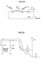
- Fig. 2B Shown in Fig. 2B is the cross-sectional view of the P-channel transistor residing in the N-well of the CMOS Off Chip Driver integrated circuit.
- the source 128, gate 130 and drain 132 having a voltage of VDD is shown for transistor 118 of Fig. 2A.
- the N-well is biased by an N+ connection to VDD at 134.
- a current path exists as shown in Fig. 2C from an external bus where a diode may be forward biased allowing current from the bus to be sunk into the N-well capacitor as well as to the decoupling capacitor 140 which may be on the order of 0.1 microfared.
- An embodiment of the invention is the CMOS Off Chip Driver for fault tolerant cold sparing shown in Fig. 3A.
- the circuit is interposed between pad signal 150 and I/O pad 152.
- a tri-state enable is performed by the combination of NAND gate 154 and NOR gate 156. This allows selection of the active state on the input/output pad 152.
- the circuit is laid out as shown in Fig. 3A wherein the pad signal goes first to a CMOS inverter formed by P-channel transistor 158 and N-channel transistor 160.
- An inverter 162 is used to drive a subsequent PMOS transistor 164.
- a final output transistor T1 drives the input/output pad 152.
- the circuit operates as follows.
- the P+/N-well and N+/P- diodes are represented by D1 and D2, respectively.
- D1 and D2 respectively.
- transistor T3 is used to bias the N-well and break the current path that would otherwise exist when VDD is equal to ground, and 5V is applied at the input/output pad 152.
- the 5V at the input/output pad is also applied to the gate of transistor T3 turning off the diode path to the VDD network through the N-well.
- T4 is used to prevent leakage through T1 to the VDD network.
- VDD is equal to ground, that is the circuit is inactive
- T4 is on and electrically connecting the gate and source of T1. This forces T1 into a high impedance mode.
- T8 is used as a switch in a similar manner to T3.
- T6 pulls the gate of T8 to ground, thus insuring normal circuit operation.
- VDD is equal to ground (inactive cold spare)
- T5 applies an I/O 5V signal to the gate of T8, preventing any leakage.
- T9 insures that a leakage path does not exist elsewhere on the pre-drive section of the Off Chip Driver which consist of transistors T8, T9, 158, 160 and 164.
- T9 As the gate potential equals ground when no power is applied T9 is turned off.
- Transistor T7 clamps the gate of complementary final drive transistor T2 to ground, preventing any leakage current.
- VDD is equal to ground
- T7 keeps the gate of T2 from rising above ground, due to capacitive coupling of any I/O transitions.
- the necessary gate drive is provided from the I/O path through T10.
- T11 shuts off T7, removing any interference with normal operations.
- All the P-channel field effect transistors required for cold sparing operation of this circuit must reside in the same N-well which is biased by T3. This is to insure that all P+ diffusions exposed to the 5V input/output signal will not have a current path to VDD through the N-well.
- the drain of T8 is also connected to the N-well providing an ohmic connection to VDD when power is applied. This insures a 5V N-well bias during normal circuit operation.
- FIG. 3B A cross-sectional view of a P-channel transistor connected across the P-channel biasing transistor T3 is shown in Fig. 3B.
- Pad 152 is connected to the gate of transistor T3 as well as the source of final drive transistor T1. As the pad voltage goes up, T3 goes off. This prevents any leakage path between the VDD network and any capacitance through capacitor 166.
- a circuit simulation of the CMOS On Chip Driver of Fig. 3A is shown in Fig. 4. Output signal point P10 is illustrated having a 5V logic swing. The current into the Off Chip Driver for cold sparing applications where VDD is equal to ground shows current spikes of approximately + 300 uA during the switching of the external net.
- the DC value of input current is zero.
- the N-well which rises and falls with the input/output signal.
- the gate voltage of the final drive transistor, T1 is shown and the gate voltage of the complementary drive transistor T2 is shown.
Landscapes
- Engineering & Computer Science (AREA)
- General Engineering & Computer Science (AREA)
- Theoretical Computer Science (AREA)
- Computer Hardware Design (AREA)
- Physics & Mathematics (AREA)
- General Physics & Mathematics (AREA)
- Logic Circuits (AREA)
- Metal-Oxide And Bipolar Metal-Oxide Semiconductor Integrated Circuits (AREA)
Claims (2)
- Circuit d'attaque hors puce CMOS comprenant :un transistor à canal P de polarisation de puits N (T3) comportant une source, un drain et une grille, la grille étant reliée à un plot d'entrée/sortie (152) et à une paire de transistors d'attaque finale CMOS (T1, T2),la ligne source-drain étant reliée entre la tension d'alimentation (VDD) et le puits N,la paire de transistors d'attaque finale CMOS (T1, T2) reliés à un circuit d'attaque CMOS de précharge (T8, T9, 158, 160, 162, 164) comportant une entrée et une sortie, les transistors d'attaque finale (T1, T2) procurant l'amplification de la sortie du circuit CMOS de précharge,un signal de plot (150) qui est appliqué à l'entrée du circuit d'attaque CMOS de précharge (T8, T9, 158, 160, 162, 164) et à une validation à trois états (154, 156), la validation à trois états sélectionnant l'état actif du plot d'entrée/sortie (152),d'où il résulte que le transistor de polarisation (T3) interrompt la ligne de courant entre le puits N et l'alimentation en tension (VDD) lorsque le circuit est dans un état non alimenté, de façon à empêcher efficacement toute fuite de courant.
- Circuit d'attaque hors puce CMOS selon la revendication 1 dans lequel les transistors de commande de fuite (T7, T10, T11) sont reliés entre la validation à trois états (154, 156) et l'un des transistors d'attaque finale CMOS (T2) afin de dissiper toute charge stockée due à l'état logique précédent du plot d'entrée/sortie.
Applications Claiming Priority (2)
| Application Number | Priority Date | Filing Date | Title |
|---|---|---|---|
| US598300 | 1990-10-16 | ||
| US07/598,300 US5117129A (en) | 1990-10-16 | 1990-10-16 | Cmos off chip driver for fault tolerant cold sparing |
Publications (3)
| Publication Number | Publication Date |
|---|---|
| EP0481329A2 EP0481329A2 (fr) | 1992-04-22 |
| EP0481329A3 EP0481329A3 (en) | 1993-01-13 |
| EP0481329B1 true EP0481329B1 (fr) | 1996-02-28 |
Family
ID=24395018
Family Applications (1)
| Application Number | Title | Priority Date | Filing Date |
|---|---|---|---|
| EP91117104A Expired - Lifetime EP0481329B1 (fr) | 1990-10-16 | 1991-10-08 | Circuit d'attaque en CMOS hors-puce pour un circuit de remplacement détaché tolérant les défauts |
Country Status (4)
| Country | Link |
|---|---|
| US (1) | US5117129A (fr) |
| EP (1) | EP0481329B1 (fr) |
| JP (1) | JP2549221B2 (fr) |
| DE (1) | DE69117420T2 (fr) |
Families Citing this family (36)
| Publication number | Priority date | Publication date | Assignee | Title |
|---|---|---|---|---|
| US5338978A (en) * | 1993-02-10 | 1994-08-16 | National Semiconductor Corporation | Full swing power down buffer circuit with multiple power supply isolation |
| US5387826A (en) * | 1993-02-10 | 1995-02-07 | National Semiconductor Corporation | Overvoltage protection against charge leakage in an output driver |
| US5381061A (en) * | 1993-03-02 | 1995-01-10 | National Semiconductor Corporation | Overvoltage tolerant output buffer circuit |
| WO1994029961A1 (fr) * | 1993-06-07 | 1994-12-22 | National Semiconductor Corporation | Protection contre les surtensions |
| US5406140A (en) * | 1993-06-07 | 1995-04-11 | National Semiconductor Corporation | Voltage translation and overvoltage protection |
| JP3433359B2 (ja) * | 1993-06-18 | 2003-08-04 | 日本テキサス・インスツルメンツ株式会社 | 低電圧出力駆動回路 |
| US5546021A (en) * | 1994-02-14 | 1996-08-13 | Motorola, Inc. | 3-state bicmos output buffer having power down capability |
| US5444397A (en) * | 1994-10-05 | 1995-08-22 | Pericom Semiconductor Corp. | All-CMOS high-impedance output buffer for a bus driven by multiple power-supply voltages |
| TW369712B (en) * | 1994-10-14 | 1999-09-11 | Ibm | Structure and method for connecting to integrated circuitry |
| US5701090A (en) * | 1994-11-15 | 1997-12-23 | Mitsubishi Denki Kabushiki Kaisha | Data output circuit with reduced output noise |
| US5629634A (en) * | 1995-08-21 | 1997-05-13 | International Business Machines Corporation | Low-power, tristate, off-chip driver circuit |
| GB2305035A (en) * | 1995-08-23 | 1997-03-26 | Motorola Gmbh | Open-drain SCSI driver with power-down protection |
| US5796260A (en) * | 1996-03-12 | 1998-08-18 | Honeywell Inc. | Parametric test circuit |
| US5867039A (en) * | 1996-05-17 | 1999-02-02 | Honeywell Inc. | CMOS output driver with p-channel substrate tracking for cold spare capability |
| US5852375A (en) * | 1997-02-07 | 1998-12-22 | Silicon Systems Research Limited | 5v tolerant I/O circuit |
| US5894230A (en) * | 1997-02-20 | 1999-04-13 | International Business Machines Corporation | Modified keeper half-latch receiver circuit |
| US6414360B1 (en) | 1998-06-09 | 2002-07-02 | Aeroflex Utmc Microelectronic Systems, Inc. | Method of programmability and an architecture for cold sparing of CMOS arrays |
| GB0003499D0 (en) * | 2000-02-15 | 2000-04-05 | Sgs Thomson Microelectronics | Circuit for providing a control signal |
| US6208178B1 (en) | 2000-02-23 | 2001-03-27 | Pericom Semiconductor Corp. | CMOS over voltage-tolerant output buffer without transmission gate |
| US6329835B1 (en) | 2000-02-23 | 2001-12-11 | Pericom Semiconductor Corp. | Quiet output buffers with neighbor sensing of wide bus and control signals |
| US6801416B2 (en) * | 2001-08-23 | 2004-10-05 | Institute Of Microelectronics | ESD protection system for high frequency applications |
| US6909659B2 (en) * | 2001-08-30 | 2005-06-21 | Micron Technology, Inc. | Zero power chip standby mode |
| US6762614B2 (en) * | 2002-04-18 | 2004-07-13 | Agilent Technologies, Inc. | Systems and methods for facilitating driver strength testing of integrated circuits |
| US20030207056A1 (en) * | 2002-05-03 | 2003-11-06 | Will Wood | Sealing element for vessel or container closures having improved barrier properties |
| US7881430B2 (en) * | 2006-07-28 | 2011-02-01 | General Electric Company | Automatic bus management |
| JP4882584B2 (ja) * | 2006-08-07 | 2012-02-22 | 富士通セミコンダクター株式会社 | 入出力回路 |
| US7859305B2 (en) * | 2006-08-07 | 2010-12-28 | Fujitsu Semiconductor Limited | Input/output circuit |
| US7411407B2 (en) * | 2006-10-13 | 2008-08-12 | Agilent Technologies, Inc. | Testing target resistances in circuit assemblies |
| JP5516449B2 (ja) | 2011-02-14 | 2014-06-11 | 富士通セミコンダクター株式会社 | 出力回路、システム、及び出力回路の制御方法 |
| US9214433B2 (en) * | 2013-05-21 | 2015-12-15 | Xilinx, Inc. | Charge damage protection on an interposer for a stacked die assembly |
| US10135443B1 (en) | 2017-08-03 | 2018-11-20 | Bae Systems Information And Electronic Systems Integration Inc. | Extended voltage range coldspare tolerant off chip driver |
| US10624246B2 (en) * | 2017-08-03 | 2020-04-14 | Bae Systems Information And Electronic Systems Integration Inc. | Apparatuses for implementing cold-sparable SerDes |
| US10854586B1 (en) * | 2019-05-24 | 2020-12-01 | Bae Systems Information And Electronics Systems Integration Inc. | Multi-chip module hybrid integrated circuit with multiple power zones that provide cold spare support |
| US10990471B2 (en) | 2019-05-29 | 2021-04-27 | Bae Systems Information And Electronic Systems Integration Inc. | Apparatus and method for reducing radiation induced multiple-bit memory soft errors |
| US11726943B2 (en) | 2020-03-06 | 2023-08-15 | Apogee Semiconductor, Inc. | Circuits and methods for enabling redundancy in an electronic system employing cold-sparing |
| US11342915B1 (en) | 2021-02-11 | 2022-05-24 | Bae Systems Information And Electronic Systems Integration Inc. | Cold spare tolerant radiation hardened generic level shifter circuit |
Family Cites Families (14)
| Publication number | Priority date | Publication date | Assignee | Title |
|---|---|---|---|---|
| US4570244A (en) * | 1980-07-28 | 1986-02-11 | Inmos Corporation | Bootstrap driver for a static RAM |
| JPS59158608A (ja) * | 1983-02-28 | 1984-09-08 | Pioneer Electronic Corp | 出力回路 |
| US4531068A (en) * | 1983-09-19 | 1985-07-23 | International Business Machines Corporation | Bus line precharging tristate driver circuit |
| US4631426A (en) * | 1984-06-27 | 1986-12-23 | Honeywell Inc. | Digital circuit using MESFETS |
| US4734752A (en) * | 1985-09-27 | 1988-03-29 | Advanced Micro Devices, Inc. | Electrostatic discharge protection device for CMOS integrated circuit outputs |
| JPS6382019A (ja) * | 1986-09-25 | 1988-04-12 | Mitsubishi Electric Corp | 相補形mos高インピ−ダンス回路 |
| US4746817A (en) * | 1987-03-16 | 1988-05-24 | International Business Machines Corporation | BIFET logic circuit |
| US4736271A (en) * | 1987-06-23 | 1988-04-05 | Signetics Corporation | Protection device utilizing one or more subsurface diodes and associated method of manufacture |
| US4777389A (en) * | 1987-08-13 | 1988-10-11 | Advanced Micro Devices, Inc. | Output buffer circuits for reducing ground bounce noise |
| US4782250A (en) * | 1987-08-31 | 1988-11-01 | International Business Machines Corporation | CMOS off-chip driver circuits |
| US4820942A (en) * | 1988-01-27 | 1989-04-11 | Advanced Micro Devices, Inc. | High-speed, high-drive output buffer circuits with reduced ground bounce |
| US4857770A (en) * | 1988-02-29 | 1989-08-15 | Advanced Micro Devices, Inc. | Output buffer arrangement for reducing chip noise without speed penalty |
| US4914318A (en) * | 1988-12-30 | 1990-04-03 | Intel Corporation | Latch circuit for a programmable logic device using dual n-type transistors |
| US5004936A (en) * | 1989-03-31 | 1991-04-02 | Texas Instruments Incorporated | Non-loading output driver circuit |
-
1990
- 1990-10-16 US US07/598,300 patent/US5117129A/en not_active Expired - Lifetime
-
1991
- 1991-10-08 DE DE69117420T patent/DE69117420T2/de not_active Expired - Fee Related
- 1991-10-08 EP EP91117104A patent/EP0481329B1/fr not_active Expired - Lifetime
- 1991-10-11 JP JP3290475A patent/JP2549221B2/ja not_active Expired - Lifetime
Also Published As
| Publication number | Publication date |
|---|---|
| DE69117420D1 (de) | 1996-04-04 |
| EP0481329A3 (en) | 1993-01-13 |
| EP0481329A2 (fr) | 1992-04-22 |
| JP2549221B2 (ja) | 1996-10-30 |
| DE69117420T2 (de) | 1996-09-19 |
| JPH04284719A (ja) | 1992-10-09 |
| US5117129A (en) | 1992-05-26 |
Similar Documents
| Publication | Publication Date | Title |
|---|---|---|
| EP0481329B1 (fr) | Circuit d'attaque en CMOS hors-puce pour un circuit de remplacement détaché tolérant les défauts | |
| US5926056A (en) | Voltage tolerant output buffer | |
| US5534795A (en) | Voltage translation and overvoltage protection | |
| US5576635A (en) | Output buffer with improved tolerance to overvoltage | |
| US6249171B1 (en) | Method and apparatus for galvanically isolating two integrated circuits from each other | |
| US4963766A (en) | Low-voltage CMOS output buffer | |
| US7486127B2 (en) | Transistor switch with integral body connection to prevent latchup | |
| US5917348A (en) | CMOS bidirectional buffer for mixed voltage applications | |
| US6300800B1 (en) | Integrated circuit I/O buffer with series P-channel and floating well | |
| US5771140A (en) | Electro-static discharge and latch-up prevention circuit | |
| US6803789B1 (en) | High voltage tolerant output buffer | |
| US5914844A (en) | Overvoltage-tolerant input-output buffers having a switch configured to isolate a pull up transistor from a voltage supply | |
| EP0714545B1 (fr) | Tampon de sortie de donnees ameliore | |
| US11251782B1 (en) | Level shifter with ESD protection | |
| US5907249A (en) | Voltage tolerant input/output buffer | |
| US6388469B1 (en) | Multiple power supply output driver | |
| US6313672B1 (en) | Over-voltage tolerant integrated circuit I/O buffer | |
| US6335637B1 (en) | Two-supply protection circuit | |
| US5867010A (en) | Circuit and method for voltage level translation utilizing a bias generator | |
| US6265931B1 (en) | Voltage reference source for an overvoltage-tolerant bus interface | |
| US6043680A (en) | 5V tolerant I/O buffer | |
| US7057450B2 (en) | Noise filter for an integrated circuit | |
| US6294943B1 (en) | Method of designing fail-safe CMOS I/O buffers whose external nodes accept voltages higher than the maximum gate oxide operating voltage | |
| US6570401B2 (en) | Dual rail power supply sequence tolerant off-chip driver | |
| GB2305793A (en) | A tri-state driver and circuit |
Legal Events
| Date | Code | Title | Description |
|---|---|---|---|
| PUAI | Public reference made under article 153(3) epc to a published international application that has entered the european phase |
Free format text: ORIGINAL CODE: 0009012 |
|
| AK | Designated contracting states |
Kind code of ref document: A2 Designated state(s): DE FR GB |
|
| 17P | Request for examination filed |
Effective date: 19920817 |
|
| PUAL | Search report despatched |
Free format text: ORIGINAL CODE: 0009013 |
|
| AK | Designated contracting states |
Kind code of ref document: A3 Designated state(s): DE FR GB |
|
| 17Q | First examination report despatched |
Effective date: 19950515 |
|
| GRAA | (expected) grant |
Free format text: ORIGINAL CODE: 0009210 |
|
| AK | Designated contracting states |
Kind code of ref document: B1 Designated state(s): DE FR GB |
|
| REF | Corresponds to: |
Ref document number: 69117420 Country of ref document: DE Date of ref document: 19960404 |
|
| ET | Fr: translation filed | ||
| PLBE | No opposition filed within time limit |
Free format text: ORIGINAL CODE: 0009261 |
|
| STAA | Information on the status of an ep patent application or granted ep patent |
Free format text: STATUS: NO OPPOSITION FILED WITHIN TIME LIMIT |
|
| 26N | No opposition filed | ||
| REG | Reference to a national code |
Ref country code: GB Ref legal event code: IF02 |
|
| PGFP | Annual fee paid to national office [announced via postgrant information from national office to epo] |
Ref country code: FR Payment date: 20051017 Year of fee payment: 15 |
|
| PGFP | Annual fee paid to national office [announced via postgrant information from national office to epo] |
Ref country code: DE Payment date: 20051130 Year of fee payment: 15 |
|
| PG25 | Lapsed in a contracting state [announced via postgrant information from national office to epo] |
Ref country code: DE Free format text: LAPSE BECAUSE OF NON-PAYMENT OF DUE FEES Effective date: 20070501 |
|
| REG | Reference to a national code |
Ref country code: FR Ref legal event code: ST Effective date: 20070629 |
|
| PG25 | Lapsed in a contracting state [announced via postgrant information from national office to epo] |
Ref country code: FR Free format text: LAPSE BECAUSE OF NON-PAYMENT OF DUE FEES Effective date: 20061031 |
|
| PGFP | Annual fee paid to national office [announced via postgrant information from national office to epo] |
Ref country code: GB Payment date: 20101025 Year of fee payment: 20 |
|
| REG | Reference to a national code |
Ref country code: GB Ref legal event code: PE20 Expiry date: 20111007 |
|
| PG25 | Lapsed in a contracting state [announced via postgrant information from national office to epo] |
Ref country code: GB Free format text: LAPSE BECAUSE OF EXPIRATION OF PROTECTION Effective date: 20111007 |