EP0481454A2 - FET MOS latéral et sa méthode de fabrication - Google Patents
FET MOS latéral et sa méthode de fabrication Download PDFInfo
- Publication number
- EP0481454A2 EP0481454A2 EP91117653A EP91117653A EP0481454A2 EP 0481454 A2 EP0481454 A2 EP 0481454A2 EP 91117653 A EP91117653 A EP 91117653A EP 91117653 A EP91117653 A EP 91117653A EP 0481454 A2 EP0481454 A2 EP 0481454A2
- Authority
- EP
- European Patent Office
- Prior art keywords
- diffused layer
- impurity diffused
- layer
- impurity
- conductivity type
- Prior art date
- Legal status (The legal status is an assumption and is not a legal conclusion. Google has not performed a legal analysis and makes no representation as to the accuracy of the status listed.)
- Granted
Links
Images




Classifications
-
- H—ELECTRICITY
- H10—SEMICONDUCTOR DEVICES; ELECTRIC SOLID-STATE DEVICES NOT OTHERWISE PROVIDED FOR
- H10D—INORGANIC ELECTRIC SEMICONDUCTOR DEVICES
- H10D30/00—Field-effect transistors [FET]
- H10D30/60—Insulated-gate field-effect transistors [IGFET]
- H10D30/601—Insulated-gate field-effect transistors [IGFET] having lightly-doped drain or source extensions, e.g. LDD IGFETs or DDD IGFETs
- H10D30/603—Insulated-gate field-effect transistors [IGFET] having lightly-doped drain or source extensions, e.g. LDD IGFETs or DDD IGFETs having asymmetry in the channel direction, e.g. lateral high-voltage MISFETs having drain offset region or extended drain IGFETs [EDMOS]
-
- H—ELECTRICITY
- H10—SEMICONDUCTOR DEVICES; ELECTRIC SOLID-STATE DEVICES NOT OTHERWISE PROVIDED FOR
- H10D—INORGANIC ELECTRIC SEMICONDUCTOR DEVICES
- H10D10/00—Bipolar junction transistors [BJT]
- H10D10/40—Vertical BJTs
- H10D10/421—Vertical BJTs having both emitter-base and base-collector junctions ending at the same surface of the body
-
- H—ELECTRICITY
- H10—SEMICONDUCTOR DEVICES; ELECTRIC SOLID-STATE DEVICES NOT OTHERWISE PROVIDED FOR
- H10D—INORGANIC ELECTRIC SEMICONDUCTOR DEVICES
- H10D30/00—Field-effect transistors [FET]
- H10D30/01—Manufacture or treatment
- H10D30/021—Manufacture or treatment of FETs having insulated gates [IGFET]
- H10D30/0221—Manufacture or treatment of FETs having insulated gates [IGFET] having asymmetry in the channel direction, e.g. lateral high-voltage MISFETs having drain offset region or extended-drain MOSFETs [EDMOS]
-
- H—ELECTRICITY
- H10—SEMICONDUCTOR DEVICES; ELECTRIC SOLID-STATE DEVICES NOT OTHERWISE PROVIDED FOR
- H10D—INORGANIC ELECTRIC SEMICONDUCTOR DEVICES
- H10D62/00—Semiconductor bodies, or regions thereof, of devices having potential barriers
- H10D62/10—Shapes, relative sizes or dispositions of the regions of the semiconductor bodies; Shapes of the semiconductor bodies
- H10D62/13—Semiconductor regions connected to electrodes carrying current to be rectified, amplified or switched, e.g. source or drain regions
- H10D62/137—Collector regions of BJTs
-
- H—ELECTRICITY
- H10—SEMICONDUCTOR DEVICES; ELECTRIC SOLID-STATE DEVICES NOT OTHERWISE PROVIDED FOR
- H10D—INORGANIC ELECTRIC SEMICONDUCTOR DEVICES
- H10D62/00—Semiconductor bodies, or regions thereof, of devices having potential barriers
- H10D62/10—Shapes, relative sizes or dispositions of the regions of the semiconductor bodies; Shapes of the semiconductor bodies
- H10D62/17—Semiconductor regions connected to electrodes not carrying current to be rectified, amplified or switched, e.g. channel regions
- H10D62/213—Channel regions of field-effect devices
- H10D62/221—Channel regions of field-effect devices of FETs
- H10D62/235—Channel regions of field-effect devices of FETs of IGFETs
-
- H—ELECTRICITY
- H10—SEMICONDUCTOR DEVICES; ELECTRIC SOLID-STATE DEVICES NOT OTHERWISE PROVIDED FOR
- H10D—INORGANIC ELECTRIC SEMICONDUCTOR DEVICES
- H10D62/00—Semiconductor bodies, or regions thereof, of devices having potential barriers
- H10D62/10—Shapes, relative sizes or dispositions of the regions of the semiconductor bodies; Shapes of the semiconductor bodies
- H10D62/17—Semiconductor regions connected to electrodes not carrying current to be rectified, amplified or switched, e.g. channel regions
- H10D62/351—Substrate regions of field-effect devices
- H10D62/357—Substrate regions of field-effect devices of FETs
- H10D62/364—Substrate regions of field-effect devices of FETs of IGFETs
- H10D62/378—Contact regions to the substrate regions
-
- H—ELECTRICITY
- H10—SEMICONDUCTOR DEVICES; ELECTRIC SOLID-STATE DEVICES NOT OTHERWISE PROVIDED FOR
- H10D—INORGANIC ELECTRIC SEMICONDUCTOR DEVICES
- H10D64/00—Electrodes of devices having potential barriers
- H10D64/20—Electrodes characterised by their shapes, relative sizes or dispositions
- H10D64/27—Electrodes not carrying the current to be rectified, amplified, oscillated or switched, e.g. gates
- H10D64/311—Gate electrodes for field-effect devices
- H10D64/411—Gate electrodes for field-effect devices for FETs
- H10D64/511—Gate electrodes for field-effect devices for FETs for IGFETs
- H10D64/514—Gate electrodes for field-effect devices for FETs for IGFETs characterised by the insulating layers
- H10D64/516—Gate electrodes for field-effect devices for FETs for IGFETs characterised by the insulating layers the thicknesses being non-uniform
Definitions
- the present invention relates to a lateral MOS FET and a manufacturing method thereof and, more particularly, to a double diffused lateral MOS FET (insulated-gate field effect transistor) applicable to a high withstand-voltage Bi-CMOS and manufacturing method thereof.
- a double diffused lateral MOS FET insulated-gate field effect transistor
- CMOS complementary MOS
- p-channel MOS transistor or n-channel MOS transistor is formed as lateral MOS FET.
- Fig. 1A shows a pattern layout of a conventional lateral p-channel MOS transistor
- Fig 1B is a sectional view taken along a line B-B of Fig. 1A.
- numeral 50 denotes an n ⁇ -type semiconductor substrate
- 51 a p-type diffused layer for drain region
- 52 a p+-type diffused layer for drain electrode connecting layer
- 53 an n-type diffused layer for channel and back gate regions
- 54 a p+-type diffused layer for source region
- 55 a gate insulating film
- 56 a gate electrode
- 57 an interlayer insulating film
- 58 a drain electrode
- 59 a source/back gate common electrode.
- the pattern is designed so that the gate electrode 56 may invariably exist between the contact portion 59a of the source/back gate common electrode 59 and drain contact portion 58a.
- the present invention is made to overcome the aforementioned drawbacks, and it is an object of the present invention to provide a lateral MOS FET and a manufacturing method thereof, in which a resistibility to electrostatic surge is improved and which can be used in a high withstand-voltage Bi-CMOS.
- a lateral MOS FET comprises: a first impurity diffused layer of a second conductivity type formed at a part of the surface of a semiconductor substrate of a first conductivity type; a second impurity diffused layer of the second conductivity type located in the first impurity diffused layer and formed so as to have a less depth from the surface of the substrate to the junction and a higher impurity concentration than those of the first impurity diffused layer; a third impurity diffused layer of the first conductivity type with a higher impurity concentration than the semiconductor substrate, which is formed at a part of the surface of the semiconductor substrate so as to surround the first impurity diffused layer and the second impurity diffused layer, while being in contact with a part of the periphery of the first impurity diffused layer; a fourth impurity diffused layer of the second conductivity type located in the third impurity diffused layer in the area where the third impurity diffused layer contacts the first impurity diffused layer, and formed to have
- a high withstand-voltage Bi-CMOS transistor device comprises: a semiconductor substrate of a second conductivity type; a buried layer of a first conductivity type with a high impurity concentration, which is formed to be buried in the semiconductor substrate; an epitaxial layer of the first conductivity type formed in the semiconductor substrate and above the buried layer; a first impurity diffused layer of the first conductivity type, that is formed along the periphery of the epitaxial layer to reach the buried layer and has the impurity concentration equal to that of the buried layer and higher than that of the epitaxial layer; a second impurity diffused layer of the second conductivity type formed at a part of the surface of the epitaxial layer; a third impurity diffused layer of the second conductivity type with a higher impurity concentration than that of the second impurity diffused layer, which is located in the second impurity diffused layer and formed to have a less depth from the surface of the epitaxial layer to the junction than the second impurity diffuse
- a high withstand-voltage Bi-CMOS transistor device comprises: a semiconductor substrate of a second conductivity type; a buried layer of a first conductivity type with a high impurity concentration, which is formed as a deep well in the semiconductor substrate; an epitaxial layer of the first conductivity type formed as a well in the buried layer; a first impurity diffused layer of the second conductivity type formed at a part of the surface of the epitaxial layer; a second impurity diffused layer of the second conductivity type with a higher impurity concentration than that of the first impurity diffused layer, which is located in the first impurity diffused layer and formed to have a less depth from the surface of the epitaxial layer to the junction than the first impurity diffused layer; a third impurity diffused layer of the first conductivity type with a higher impurity concentration than that of the epitaxial layer, which is formed at the surface of the epitaxial layer to surround the first impurity diffused layer and second impurity diffuse
- a method of manufacturing a lateral MOF FET according to the present invention comprises the steps of: forming a drain region by injecting impurities of a second conductivity type into the drain forming region of a semiconductor substrate of a first conductivity type and then diffusing them; forming gate insulating films in the back gate forming region, the drain electrode connecting layer forming region, and the source forming region on the semiconductor substrate; forming a gate electrode by depositing a polysilicon film over the entire surface and then patterning the deposited film; forming a back gate region by injecting impurities of the first conductivity type into the back gate forming region with the gate electrode as a mask and then diffusing the impurities; forming a drain electrode contact layer and source region by injecting impurities of the second conductivity type into the drain electrode contact forming region and source forming region and then diffusing the impurities; depositing an interlayer insulating film over the entire surface and then making openings for a source/back gate common electrode and a drain electrode; and forming a
- a part of whose surface is a channel region is formed to surround the drain region, while being in contact with a part of the periphery of the drain region.
- Fig. 3A is a plan view showing a plan pattern of a first embodiment of a lateral MOS FET according to of the present invention
- Fig. 3B is a sectional view taken along a line X-X of Fig. 3A.
- reference character Ba denotes a back gate contact portion; Da, a drain contact portion; Sa, a source contact portion; and G, a gate electrode.
- the back gate contact portion Ba is provided around the drain contact portion Da.
- the source contact portion Sa is in contact with a part of the back gate contact portion Ba for common use.
- a semiconductor substrate 10 of a first conductivity type i.e., n-type in the present invention
- the substrate 10 is made of, e.g., a silicon monocrystalline substrate.
- a drain region 11 is a first impurity diffused layer of a second conductivity type, i.e., p-type in the present invention, which is formed on the surface of the semiconductor substrate 10.
- a drain electrode connecting layer 12 is a second impurity diffused layer of a p+-type.
- the connecting layer 12 is located within the first impurity diffused layer 11 and has a less depth from the surface of the substrate 10 to the junction and has a higher impurity concentration than that of the diffused layer 11.
- a back gate region 13 is a third impurity diffused layer of an n-type with a higher impurity concentration than that of the semiconductor substrate 10. The back gate region 13 surrounds the first and second impurity diffused layers 11 and 12 on the surface of the semiconductor substrate 10, while being in contact with a part of the periphery of the first impurity diffused layer 11.
- a source region 14 is a fourth impurity diffused layer of a p+-type.
- the source region 14 is located in the third impurity diffused layer 13 in the area where the third impurity diffused layer 13 is in contact with the first impurity diffused layer 11.
- the source region 14 has a less depth from the surface of the substrate 10 to the junction than that of the third impurity diffused layer 13 and has a higher impurity concentration than that of the first impurity diffused layer 11.
- a gate electrode G is formed via a gate insulating film 15 on the channel region CH which is the surface region of the third impurity diffused layer 13 intervened between the fourth and first impurity diffused layers 14 and 11.
- the gate insulating film 15 is made of, for example, silicon dioxide (SiO2) film.
- a drain electrode D is formed in contact with the second impurity diffused layer 12.
- a source/back gate common electrode SB is isolated from the drain contact portion Da while surrounding it, as shown in Fig. 3A, and is in contact with both the third and fourth impurity diffused layers 13 and 14, as shown in Fig. 3B.
- An interlayer insulating film 16 is formed of SiO2, for example.
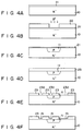
- Figs. 4A through 4M a manufacturing method of the lateral p-channel MOS transistor in Fig. 3 will be described in detail.
- an insulating film 21 is formed by dry oxidation at 1000°C on the surface of the n ⁇ -type silicon substrate 10.
- the insulating film 21 is made of SiO2 film of 0.1 ⁇ m thickness, for example.
- a photoresist pattern 22 is formed on the surface by photoetching. Then p-type impurities are injected into the entire surface by ion implantation. Boron ion is used as the p-type impurity.
- borons are diffused by heat treatment at 1200°C to form the p-type impurity diffused layer 11.
- the diffused layer 11 is used as the drain region.
- an insulating film (SiO2) 23 is then grown to a thickness of 1.0 ⁇ m on the surface by steam oxidation at 1000°C.
- openings 23a are formed by removing predetermined areas of the insulating film 23 by means of photoetching.
- gate insulating films 15 are formed on the bottom of the openings 23a by dry oxidation at 1000°C.
- the gate insulating film 15 is made of SiO2 film of 0.1 ⁇ m thickness, for example.
- a polysilicon film is deposited to a thickness of 0.5 ⁇ m on the entire surface of the substrate by chemical vapor deposition (CVD). Then, the polysilicon film is patterned by photoetching to thus form the gate electrode G.
- CVD chemical vapor deposition
- a photoresist pattern 24 is formed on the resultant surface by photoetching.
- N-type impurity ions are injected into the entire surface by ion implantation, using the photoresist pattern and the gate electrode G as a mask.
- Phosphorus ion P+ is used as the n-type impurity ion, for example.
- phosphori are diffused by heat treatment at 1200°C to form the n-type impurity diffused layer 13.
- the diffused layer 13 is used as the back gate region.
- a photoresist pattern 25 is formed by photoetching on the surface. Then, boron ions B+ are implanted into the entire surface by ion implantation, using the photoresist pattern 25, the gate electrode G and the insulating film 23 as a mask.
- an interlayer insulating film (SiO2) 16 is deposited to a thickness of 1.0 ⁇ m by CVD on the entire surface. Then, the interlayer insulating film 16 is annealed by heat treatment at 1000°C. Borons are diffused by the same heat treatment to form the p+-type impurity diffused layer 12 and the impurity diffused layer 14. The diffused layers 12 and 14 are used as the drain electrode connecting layer and the source region, respectively.
- contact holes are formed by removing predetermined areas of the interlayer insulating film 16 by means of photoetching. These contact holes correspond to the back gate contact portion Ba, the drain contact portion Da, and the source contact portion Sa.
- a metal wiring film such as Al film is deposited to a thickness of 1.0 ⁇ m over the surface of the resultant structure.
- the metal wiring film is then patterned by photoetching to form the drain electrode D and the source/back gate common electrode SB.
- the drain electrode D is in contact with the impurity diffused layer 12 as the drain electrode connecting layer.
- the common electrode SB is in contact not only with the whole back gate region 13 but also with the source region 14 which is formed in the area of the back gate region 13. After this, sintering is executed to complete the lateral MOS FET of Fig. 3B.
- the back gate region 13 is formed so as to surround the drain region 11 while being in contact with a part of the drain region 11. This arrangement allows a surge current to disperse from the drain region 11 to the surrounding back gate region 13. This suppresses a rise in the electric potential at the drain region 11. As a result, the electric potential value rarely exceeds the dielectric strength of the gate insulting film 15. Thus, a breakdown of the gate insulating film 15 and therefore an electrostatic breakdown of the device are suppressed .
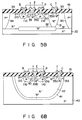
- Fig. 5A is a sectional view showing a lateral p-channel MOS FET according to a second embodiment of the present invention.
- Fig. 5A shows a sectional structure of the MOS FET as an integrated circuit.
- a lateral p-channel MOS transistor is formed on an island of an n ⁇ -type epitaxial layer 33 which is surrounded by a deep n+-type diffused layer 31 and an n+-type buried layer 32 formed in a p ⁇ -type substrate 30. More particulary, first the n+-type buried layer 32 is formed in the p ⁇ -type substrate 30 and the n ⁇ -type epitaxial layer 33 is formed on the substrate 30 and the layer 32.
- a p+-type semiconductor region 34 as an element isolation region is formed in outer part of the n ⁇ -type epitaxial layer 33. Further, in another part of the n ⁇ -type epitaxial layer 33, the deep n+-type diffused layer 31 reaching the n+-type buried layer 32 is formed. On the n ⁇ -type epitaxial layer 33 surrounded by both the deep n+-type diffused layer 31 and n+-type buried layer 32, the p-type diffused layer 11 is formed as the drain region. The n-type diffused layer 13 is then formed as the channel region/back gate region.
- the diffused layer 13 is in contact with part of the periphery of the p-type diffused layer 11 and be partially located in the deep n+-type diffused layer 31.
- An n-type diffused layer 13a i.e. a part of the n-type diffused layer 13, is formed as the back gate region so as to be located in the deep n+-type diffused layer 31 in a manner to surround the p-type diffused layer 11.
- numeral 12 denotes a p+-type diffused layer as the drain electrode connecting layer; 14, a p+-type diffused layer as the source region; 15, the gate insulating film; G, the gate electrode; D, the drain electrode; SB, the source/back gate common electrode; 16, the interlayer insulating film; and 35, an n+-type diffused layer as the back gate electrode connecting layer.
- Fig. 5B shows a sectional structure of a bipolar device as an integrated circuit which is formed on the same p ⁇ -type substrate 30 as shown in Fig. 5A.
- the p ⁇ -type substrate 30, a deep n+-type diffused layer 31 as a buried collector electrode connecting layer, an n+-type buried layer 32 as a collector buried electrode, an n ⁇ -type epitaxial layer 33, and a p+-type semiconductor region 34 as a device isolation region are formed by the same steps as those in Fig. 5A.
- an interlayer insulating film 16 is identical to that of Fig. 5A.
- a p-type diffused layer 11a as an external base region and a p+-type diffused layer 12a as a base electrode connecting layer are formed simultaneously with the drain region 11 and the drain electrode connecting layer 12 in Fig. 5A, respectively.
- An n+-type diffused layer 35a as a collector electrode connecting layer and n+-type diffused layer 35b as an emitter region are formed at the same time as the back gate electrode connecting layer 35 in Fig. 5A.
- a p-type diffused region 39 as a base region is formed between the steps for forming the external base region 11a and the emitter region 35b.
- boron ions are injected as p-type impurity by ion implantation using another photoresist mask and then diffused simultaneously with the n-type diffused layer 13 in Fig. 5A.
- a base electrode B, an emitter electrode E, and a collector electrode C are formed simultaneously with the drain electrode D and the source/back gate common electrode SB in Fig. 5A.
- Fig. 6A is a sectional view showing a lateral p-channel MOS FET according to a third embodiment of the present invention.
- Fig. 6A also shows a sectional structure of the MOS FET as an integrated circuit.
- a lateral p-channel MOS transistor is formed on an island of a deep n ⁇ -type buried epitaxial layer 42 which is surrounded by an n+-type buried layer 41 on a p ⁇ -type substrate 40. More particulary, the convex n+-type buried layer 41 is first formed deeply in the p ⁇ -type substrate 40 and the n ⁇ -type buried epitaxial layer 42 is formed in the buried layer 41.
- a p-type diffused layer 11 is formed as the drain region in the epitaxial layer 42.
- An n-type diffused layer 13 is formed as the channel region/back gate region.
- the diffused layer 13 is in contact with part of the periphery of the p-type diffused layer 11 at the surface of the n ⁇ -type epitaxial layer 42, while being partially located in the n+-type buried layer 41.
- the n-type diffused layer 13a i.e., a part of the n-type diffused layer 13, is formed as the back gate region at a part of the surface of the n ⁇ -type epitaxial layer 42 and at the surface of the n+-type buried layer 41 so as to surround the p-type diffused layer 11.
- numeral 12 denotes a p+-type diffused layer as the drain electrode connecting layer; 14, a p+-type diffused layer as the source region; 15, the gate insulating film; G, the gate electrode; D, the drain electrode; SB, the source/back gate common electrode; 16, the interlayer insulting film,; and 35, an n+-type diffused layer as the back gate electrode connecting layer.
- Fig. 6B shows a sectional structure of a bipolar device as an integrated circuit which is also formed on the same p ⁇ -type substrate 40 as shown in Fig. 6A.
- the p ⁇ -type substrate 40, an n+-type buried layer 41 as a collector buried electrode, and a deep n ⁇ -type buried epitaxial layer 42 are formed by the same steps as those in Fig. 6A.
- An interlayer insulating film 16 is also identical to that of Fig. 6A.
- a p-type diffused layer 11a as an external base region, and an n-type diffused layer 13a are formed simultaneously with the drain region 11 and the channel region/back gate region 13 in Fig. 6A, respectively.
- a p+-type diffused layer 12a as a base electrode connecting layer is formed at the same time as the drain electrode connecting layer 12 in Fig. 6A.
- An n+-type diffused layer 35a as a collector electrode connecting layer and an n+-type diffused layer 35b as an emitter region are formed simultaneously with the back gate electrode connecting layer 35 in Fig. 6A.
- a p-type diffused region 45 as a base region is formed after the external base region 11a is formed. Born ions are implanted and diffused simultaneously with the layer 13a to thus form the base region 45.
- a base electrode B, an emitter electrode E and a collector electrode C are also formed simultaneously with the drain electrode D and the source/back gate common electrode SB in Fig. 6A.
- lateral MOS FETs With lateral MOS FETs according to the present invention, it is possible to improve the resistibility to an electrostatic surge.
- a lateral MOS FET of the present invention can achieve the resistibility to an electrostatic surge of more than one thousand voltages, for example.
Landscapes
- Insulated Gate Type Field-Effect Transistor (AREA)
- Thin Film Transistor (AREA)
Applications Claiming Priority (2)
| Application Number | Priority Date | Filing Date | Title |
|---|---|---|---|
| JP280202/90 | 1990-10-17 | ||
| JP2280202A JP2609753B2 (ja) | 1990-10-17 | 1990-10-17 | 半導体装置 |
Publications (3)
| Publication Number | Publication Date |
|---|---|
| EP0481454A2 true EP0481454A2 (fr) | 1992-04-22 |
| EP0481454A3 EP0481454A3 (en) | 1992-10-21 |
| EP0481454B1 EP0481454B1 (fr) | 1997-12-10 |
Family
ID=17621734
Family Applications (1)
| Application Number | Title | Priority Date | Filing Date |
|---|---|---|---|
| EP91117653A Expired - Lifetime EP0481454B1 (fr) | 1990-10-17 | 1991-10-16 | MOSFET latéral et sa méthode de fabrication |
Country Status (5)
| Country | Link |
|---|---|
| US (1) | US5306938A (fr) |
| EP (1) | EP0481454B1 (fr) |
| JP (1) | JP2609753B2 (fr) |
| KR (1) | KR950009795B1 (fr) |
| DE (1) | DE69128406T2 (fr) |
Cited By (3)
| Publication number | Priority date | Publication date | Assignee | Title |
|---|---|---|---|---|
| US5565367A (en) * | 1995-03-24 | 1996-10-15 | Hualon Micro Electronic Corporation | Protective device for an integrated circit and manufacturing method thereof |
| EP0708486A3 (fr) * | 1994-10-17 | 1997-07-02 | Nec Corp | Transistor semi-conducteur à effet de champ à région étendue en contact avec le substrat |
| WO2010081705A1 (fr) | 2009-01-13 | 2010-07-22 | Saipem. S.P.A. | Procédé pour l'obtention de 1-butène de haute pureté à partir de mélanges d'hydrocarbures en c4 |
Families Citing this family (8)
| Publication number | Priority date | Publication date | Assignee | Title |
|---|---|---|---|---|
| JP2001110810A (ja) * | 1999-10-06 | 2001-04-20 | Fujitsu Ltd | 半導体装置及びその製造方法 |
| JP3831602B2 (ja) | 2000-12-07 | 2006-10-11 | 三洋電機株式会社 | 半導体装置の製造方法 |
| US6969909B2 (en) * | 2002-12-20 | 2005-11-29 | Vlt, Inc. | Flip chip FET device |
| US7038917B2 (en) * | 2002-12-27 | 2006-05-02 | Vlt, Inc. | Low loss, high density array interconnection |
| KR100722700B1 (ko) * | 2004-03-26 | 2007-05-30 | 산켄덴키 가부시키가이샤 | 반도체장치 |
| JP5180468B2 (ja) * | 2006-12-21 | 2013-04-10 | オンセミコンダクター・トレーディング・リミテッド | 半導体装置及びその製造方法 |
| JP5586546B2 (ja) * | 2011-03-23 | 2014-09-10 | 株式会社東芝 | 半導体装置 |
| US9660053B2 (en) * | 2013-07-12 | 2017-05-23 | Power Integrations, Inc. | High-voltage field-effect transistor having multiple implanted layers |
Family Cites Families (8)
| Publication number | Priority date | Publication date | Assignee | Title |
|---|---|---|---|---|
| US4300150A (en) * | 1980-06-16 | 1981-11-10 | North American Philips Corporation | Lateral double-diffused MOS transistor device |
| US4661838A (en) * | 1985-10-24 | 1987-04-28 | General Electric Company | High voltage semiconductor devices electrically isolated from an integrated circuit substrate |
| JPH01179342A (ja) * | 1988-01-05 | 1989-07-17 | Toshiba Corp | 複合半導体結晶体 |
| DE68918783T2 (de) * | 1988-08-18 | 1995-03-30 | Seiko Epson Corp | MIS-Bauelement. |
| EP0371785B1 (fr) * | 1988-11-29 | 1996-05-01 | Kabushiki Kaisha Toshiba | MOSFET latéral à modulation de conductivité |
| JP2509690B2 (ja) * | 1989-02-20 | 1996-06-26 | 株式会社東芝 | 半導体装置 |
| JPH02237159A (ja) * | 1989-03-10 | 1990-09-19 | Toshiba Corp | 半導体装置 |
| US5146298A (en) * | 1991-08-16 | 1992-09-08 | Eklund Klas H | Device which functions as a lateral double-diffused insulated gate field effect transistor or as a bipolar transistor |
-
1990
- 1990-10-17 JP JP2280202A patent/JP2609753B2/ja not_active Expired - Fee Related
-
1991
- 1991-10-16 US US07/777,004 patent/US5306938A/en not_active Expired - Lifetime
- 1991-10-16 EP EP91117653A patent/EP0481454B1/fr not_active Expired - Lifetime
- 1991-10-16 DE DE69128406T patent/DE69128406T2/de not_active Expired - Fee Related
- 1991-10-17 KR KR1019910018251A patent/KR950009795B1/ko not_active Expired - Fee Related
Cited By (3)
| Publication number | Priority date | Publication date | Assignee | Title |
|---|---|---|---|---|
| EP0708486A3 (fr) * | 1994-10-17 | 1997-07-02 | Nec Corp | Transistor semi-conducteur à effet de champ à région étendue en contact avec le substrat |
| US5565367A (en) * | 1995-03-24 | 1996-10-15 | Hualon Micro Electronic Corporation | Protective device for an integrated circit and manufacturing method thereof |
| WO2010081705A1 (fr) | 2009-01-13 | 2010-07-22 | Saipem. S.P.A. | Procédé pour l'obtention de 1-butène de haute pureté à partir de mélanges d'hydrocarbures en c4 |
Also Published As
| Publication number | Publication date |
|---|---|
| JP2609753B2 (ja) | 1997-05-14 |
| DE69128406T2 (de) | 1998-04-30 |
| KR920008967A (ko) | 1992-05-28 |
| EP0481454B1 (fr) | 1997-12-10 |
| JPH04154173A (ja) | 1992-05-27 |
| DE69128406D1 (de) | 1998-01-22 |
| KR950009795B1 (ko) | 1995-08-28 |
| EP0481454A3 (en) | 1992-10-21 |
| US5306938A (en) | 1994-04-26 |
Similar Documents
| Publication | Publication Date | Title |
|---|---|---|
| US6392275B1 (en) | Semiconductor device with DMOS, BJT and CMOS structures | |
| US5420061A (en) | Method for improving latchup immunity in a dual-polysilicon gate process | |
| US5374569A (en) | Method for forming a BiCDMOS | |
| US5648281A (en) | Method for forming an isolation structure and a bipolar transistor on a semiconductor substrate | |
| US4939099A (en) | Process for fabricating isolated vertical bipolar and JFET transistors | |
| JPH08227945A (ja) | BiCDMOSプロセスに基づく集積回路形成方法 | |
| US6570229B1 (en) | Semiconductor device | |
| US6005283A (en) | Complementary bipolar transistors | |
| KR910006672B1 (ko) | 반도체 집적회로 장치 및 그의 제조 방법 | |
| EP0481454B1 (fr) | MOSFET latéral et sa méthode de fabrication | |
| US5869850A (en) | Lateral insulated gate bipolar transistor | |
| US6376870B1 (en) | Low voltage transistors with increased breakdown voltage to substrate | |
| TWI408779B (zh) | 半導體裝置之形成方法及其結構 | |
| KR940003378B1 (ko) | 전하전송 디바이스를 포함하는 반도체장치 및 그 제조방법 | |
| EP0423791B1 (fr) | Elément capacitif du type MIS | |
| US20060027895A1 (en) | Forming lateral bipolar junction transistor in CMOS flow | |
| EP0399454B1 (fr) | Dispositif semi-conducteur monolithique comprenant des structures ccd, bipolaires et mos | |
| US5047820A (en) | Semi self-aligned high voltage P channel FET | |
| US20030001199A1 (en) | Electrostatic discharge protection in double diffused MOS transistors | |
| US6011283A (en) | Pillar emitter for BiCMOS devices | |
| US5744855A (en) | Single-poly-type bipolar transistor | |
| EP0348626B1 (fr) | Procédé pour l'intégration de transistors isolés bipolaires verticaux et JFET et circuit intégré correspondant | |
| JP3077742B2 (ja) | 半導体装置及びその製造方法 | |
| KR930008022B1 (ko) | 반도체장치 | |
| US6110767A (en) | Reversed MOS |
Legal Events
| Date | Code | Title | Description |
|---|---|---|---|
| PUAI | Public reference made under article 153(3) epc to a published international application that has entered the european phase |
Free format text: ORIGINAL CODE: 0009012 |
|
| 17P | Request for examination filed |
Effective date: 19911016 |
|
| AK | Designated contracting states |
Kind code of ref document: A2 Designated state(s): DE FR GB |
|
| PUAL | Search report despatched |
Free format text: ORIGINAL CODE: 0009013 |
|
| AK | Designated contracting states |
Kind code of ref document: A3 Designated state(s): DE FR GB |
|
| 17Q | First examination report despatched |
Effective date: 19941201 |
|
| GRAG | Despatch of communication of intention to grant |
Free format text: ORIGINAL CODE: EPIDOS AGRA |
|
| GRAG | Despatch of communication of intention to grant |
Free format text: ORIGINAL CODE: EPIDOS AGRA |
|
| GRAH | Despatch of communication of intention to grant a patent |
Free format text: ORIGINAL CODE: EPIDOS IGRA |
|
| GRAH | Despatch of communication of intention to grant a patent |
Free format text: ORIGINAL CODE: EPIDOS IGRA |
|
| GRAA | (expected) grant |
Free format text: ORIGINAL CODE: 0009210 |
|
| AK | Designated contracting states |
Kind code of ref document: B1 Designated state(s): DE FR GB |
|
| REF | Corresponds to: |
Ref document number: 69128406 Country of ref document: DE Date of ref document: 19980122 |
|
| ET | Fr: translation filed | ||
| REG | Reference to a national code |
Ref country code: GB Ref legal event code: 746 Effective date: 19980910 |
|
| PLBE | No opposition filed within time limit |
Free format text: ORIGINAL CODE: 0009261 |
|
| STAA | Information on the status of an ep patent application or granted ep patent |
Free format text: STATUS: NO OPPOSITION FILED WITHIN TIME LIMIT |
|
| 26N | No opposition filed | ||
| REG | Reference to a national code |
Ref country code: FR Ref legal event code: D6 |
|
| REG | Reference to a national code |
Ref country code: GB Ref legal event code: IF02 |
|
| PGFP | Annual fee paid to national office [announced via postgrant information from national office to epo] |
Ref country code: GB Payment date: 20021016 Year of fee payment: 12 |
|
| PGFP | Annual fee paid to national office [announced via postgrant information from national office to epo] |
Ref country code: DE Payment date: 20021017 Year of fee payment: 12 |
|
| PG25 | Lapsed in a contracting state [announced via postgrant information from national office to epo] |
Ref country code: GB Free format text: LAPSE BECAUSE OF NON-PAYMENT OF DUE FEES Effective date: 20031016 |
|
| PG25 | Lapsed in a contracting state [announced via postgrant information from national office to epo] |
Ref country code: DE Free format text: LAPSE BECAUSE OF NON-PAYMENT OF DUE FEES Effective date: 20040501 |
|
| GBPC | Gb: european patent ceased through non-payment of renewal fee |
Effective date: 20031016 |
|
| PGFP | Annual fee paid to national office [announced via postgrant information from national office to epo] |
Ref country code: FR Payment date: 20051010 Year of fee payment: 15 |
|
| REG | Reference to a national code |
Ref country code: FR Ref legal event code: ST Effective date: 20070629 |
|
| PG25 | Lapsed in a contracting state [announced via postgrant information from national office to epo] |
Ref country code: FR Free format text: LAPSE BECAUSE OF NON-PAYMENT OF DUE FEES Effective date: 20061031 |