EP0481487A2 - Bereitschaftsbetriebsteuerschaltung - Google Patents
Bereitschaftsbetriebsteuerschaltung Download PDFInfo
- Publication number
- EP0481487A2 EP0481487A2 EP91117750A EP91117750A EP0481487A2 EP 0481487 A2 EP0481487 A2 EP 0481487A2 EP 91117750 A EP91117750 A EP 91117750A EP 91117750 A EP91117750 A EP 91117750A EP 0481487 A2 EP0481487 A2 EP 0481487A2
- Authority
- EP
- European Patent Office
- Prior art keywords
- stand
- mosfet
- control circuit
- gate
- signal
- Prior art date
- Legal status (The legal status is an assumption and is not a legal conclusion. Google has not performed a legal analysis and makes no representation as to the accuracy of the status listed.)
- Withdrawn
Links
Images
Classifications
-
- G—PHYSICS
- G01—MEASURING; TESTING
- G01R—MEASURING ELECTRIC VARIABLES; MEASURING MAGNETIC VARIABLES
- G01R31/00—Arrangements for testing electric properties; Arrangements for locating electric faults; Arrangements for electrical testing characterised by what is being tested not provided for elsewhere
- G01R31/28—Testing of electronic circuits, e.g. by signal tracer
- G01R31/30—Marginal testing, e.g. by varying supply voltage
- G01R31/3004—Current or voltage test
-
- G—PHYSICS
- G06—COMPUTING OR CALCULATING; COUNTING
- G06F—ELECTRIC DIGITAL DATA PROCESSING
- G06F1/00—Details not covered by groups G06F3/00 - G06F13/00 and G06F21/00
- G06F1/26—Power supply means, e.g. regulation thereof
- G06F1/32—Means for saving power
Definitions
- This invention relates to a stand-by control circuit, and more particularly to, a stand-by control circuit for controlling a low power consumption operation mode called as a stand-by mode of a microcomputer.
- microcomputers have been applied to machines such as office automation machines.
- Microcomputers used in such machines are required to have a performance of low power consumption, because the machines are applied with a power supply from batteries equipped in the machines in accordance with tendencies of small size and light weight thereof.
- microcomputers are programmed to operate with low power consumption mode called as "stand-by mode".
- stand-by mode the microcomputer halts its processing operation with maintaining information of internal states of the microcomputer in registers, flags, RAMs, etc.
- the microcomputer goes into the stand-by mode by carrying out a stand-by control command, and is released from the stand-by mode by receiving a system reset signal.
- a conventional stand-by control circuit for controlling stand-by mode operation of a microcomputer includes a stand-by flag of a set/reset type flip-flop, a power ON detecting circuit which supplies a power ON detecting signal to a reset input terminal of the stand-by flag, an AND gate which has two input terminals supplied with a writing signal and a signal of a bus line, and a bus driver which is supplied with an output signal of the stand-by flag and controlled by a reading signal to supply a stand-by signal to the bus line.
- the power ON detecting circuit usually includes a transistor which is maintained to be at ON state.
- the power ON detecting circuit detects the power ON state and the power ON detecting signal becomes active to be supplied to the stand-by flag to reset.
- the stand-by flag is set when the AND gate supplies a set signal of logic level "1" on condition that the writing signal is active and the bus line is high level.
- An output signal of the stand-by flag is supplied to the bus line through the bus driver when a reading signal supplied to the bus driver becomes active.
- the power ON detecting signal supplied from the power ON detecting circuit becomes active, just after the power supply is turned on and remains active until the power supply voltage becomes as high as the inversion level, then the power ON detecting signal becomes inactive. In such operation, a constant current flows through the transistor which is maintained at ON state in the power ON detecting circuit.
- the stand-by flag is controlled to be at a set state, when a system is reset after the release of the stand-by mode, while the stand-by flag is controlled to be at a reset state, when the system is reset by turning a power supply on, so that the two reset states of the system are easily distinguished.
- a stand-by control circuit comprises; means for detecting a state of a power supply; a flag which is reset by a power ON detecting signal supplied from the detecting means; wherein the detecting means comprises means for shutting off a current flowing through the detecting means during a testing mode carried out in accordance with a testing signal.
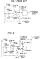
- the conventional stand-by control circuit includes a stand-by flag 31 of a set/reset type flip-flop, a power ON detecting circuit 32 which supplies a power ON detecting signal 33 to a reset input terminal of the stand-by flag 31, an AND gate 34 which has two input terminals supplied with a stand-by flag writing signal (SBFW) 35 and a signal of a bus line 38, and a bus driver 36 which is supplied with an output signal of the stand-by flag 31 and controlled by a stand-by flag reading signal (SBFR) 37 to supply a stand-by signal to the bus line 38.
- the power ON detecting circuit 32 usually includes a transistor which is maintained to be at ON state.
- the power ON detecting circuit 32 detects the power ON state to supply a power ON detecting signal to the stand-by flag 31 which is thereby reset.
- the stand-by flag 31 is set when the AND gate 34 supplies a set signal of logic level "1" on condition that the writing signal 35 is active and the bus line 38 is high level.
- An output signal of the stand-by flag 31 is supplied to the bus line 38 through the bus driver 36 when a reading signal 37 supplied to the bus driver 36 becomes active.
- the power ON detecting signal 33 supplied from the power ON detecting circuit 32 becomes active in accordance with the change of a logic threshold voltage at the time of turning the power supply ON, just after the power supply is turned on, and the power ON detecting signal 33 becomes inactive, when the power supply voltage becomes as high as the inversion level.
- a constant current flows through the transistor of the constantly ON state in the power ON detecting circuit 32.
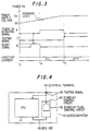
- the stand-by control circuit includes a stand-by flag 1 of a set/reset type flip-flop, a P-MOSFET 2, AN N-MOSFET 3, A NOR gate 5, an AND gate 8, and a bus driver 10.
- the P-MOSFET 2 is connected at a gate to a testing signal line 7, at a source to a power supply level, and at a nodal point B.
- the N-MOSFET 3 is connected at a gate to the power supply level, at a source to ground, and at a drain to the nodal point B.
- the NOR gate 5 is connected at two input terminals to the testing signal line 7 and the nodal point B, and at an output terminal to a reset terminal of the stand-by flag 1.
- the AND gate 8 is connected at two input terminals to a writing signal line 9 and a nodal point A.
- the stand-by flag 1 is connected at an output terminal to an input terminal of the bus driver 10.
- the bus driver 10 is connected at a control terminal to a reading signal line 11 and at an output terminal to the nodal point A.
- the testing signal is inactive, so that the P-MOSFET 2 is at ON state.
- the power supply is turned on (time t1 ), so that the power supply voltage increases gradually, as shown in Fig. 3, and the N-MOSFET 3 is turned on.
- the power ON detecting signal level which is a voltage level of the nodal point B is maintained to be low level until the power supply voltage becomes the inversion level. Therefore, the NOR gate 5 is supplied with two low level input signals, so that the NOR gate 5 supplies a high level signal to the reset terminal of the stand-by flag 1 to be reset.
- the power ON detecting signal becomes high level (time t2 ), so that the NOR gate 5 supplies a low level signal to the stand-by flag 1.
- the stand-by flag 1 is set when the AND gate 8 supplies a set signal of logic level "1" on condition that the stand-by flag writing signal (SBFW) 9 is active and the bus line 12 is at a high level.
- An output signal of the stand-by flag 1 is supplied to the bus line 12 through the bus driver 10 when a stand-by flag reading signal (SBFR) 11 supplied to the bus driver 10 becomes active.
- SBFR stand-by flag reading signal
- the testing signal is set to be high (time t 3 ), so that the P-MOSFET 2 becomes at OFF state. Therefore, no current flows through the P-MOSFET 2 and the N-MOSFET 3, and the power ON detecting signal becomes low level.
- the NOR gate 5 is supplies with a high level, so that it supplies the reset terminal of the stand-by flag with a low level signal. After the time t2 , no constant current flows through the P- and N-MOSFETs 2 and 3.
- the testing signal may be supplied from an external terminal of the microcomputer, or may be supplied form a testing mode changing circuit provided in the microcomputer.
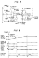
- Fig. 4 shows a microcomputer 40 including the stand-by control circuit in the first preferred embodiment.
- a stand-by flag control circuit 42 which is included in the stand-by control circuit 43 is supplied with a testing signal 45 through an external terminal 44 of the microcomputer 40.
- a CPU 41 of the microcomputer 40 and the stand-by control circuit 43 are connected each other by a bus line 49. The CPU 41 is also supplied with the testing signal 45.
- the microcomputer 40 has a testing mode as well as an ordinary operation mode for operating command processes. Switching of the two modes are determined by the testing signal 45 which is determined by an input logic level of the external terminal 44.
- the ordinary operation mode is selected when the input logic level thereof is "0", and the testing mode is selected when the input logic level thereof is "1".
- the testing signal 45 is supplied directly from the external terminal 44, however, the testing signal 45 may be supplied from a register for storing a data determining a testing mode in the microcomputer 40.
- the stand-by control circuit includes a stand-by flag 13 of a set/reset type flip-flop, a P-MOSFET 14, two N-MOSFETs 15 and 19, two inverters 17 and 20, an AND gate 22, and a bus driver 24.
- the P-MOSFET 14 is connected at a gate to ground, at a source to a power supply level, and at a drain to a nodal point D.
- the N-MOSFET 19 is connected at a gate to the testing signal line 21 through the inverter 20, at a source to a drain of the N-MOSFET 15, and at a drain to the nodal point D.
- the N-MOSFET 15 is connected at a gate to the power supply level, at a source to ground.
- the stand-by flag 13 is connected at a reset terminal to the nodal point D through the inverter 17, at a set terminal to an output of the AND gate 22, and at an output terminal to a nodal point C through the bus driver 24.
- the AND gate 22 is connected at two input terminals to a writing signal line 23 and a nodal point C.
- the bus driver 24 is connected at a control terminal to a reading signal line 25.
- the testing signal is set to be inactive, so that the N-MOSFET 19 is applied at the gate with a high level to be at ON state.
- the power supply voltage increases gradually, as shown in Fig. 6, and the N-MOSFET 15 becomes ON state.
- the P-MOSFET 14 is constantly at ON state.
- the power ON detecting signal level which is a voltage level of the nodal point D is maintained to be low level until the power supply voltage becomes the inversion level (time t2 ).
- the stand-by flag 13 is supplied at the reset terminal with a high level signal through the inverter 17 to be reset.
- the power detecting signal becomes high level, so that the stand-by flag 13 is supplied at the reset terminal with a low level.
- the stand-by flag 13 is set when the AND gate 22 supplies a set signal of logic level "1" on condition that the writing signal (SPFW) 23 is active and the bus line 26 is high level.
- An output signal of the stand-by flag 13 is supplied to the bus line 26 through the bus driver 24 when a reading signal (SPFR) 25 supplied to the bus driver 24 becomes active.
Landscapes
- Engineering & Computer Science (AREA)
- Physics & Mathematics (AREA)
- General Engineering & Computer Science (AREA)
- General Physics & Mathematics (AREA)
- Theoretical Computer Science (AREA)
- Microcomputers (AREA)
- Electronic Switches (AREA)
Applications Claiming Priority (2)
| Application Number | Priority Date | Filing Date | Title |
|---|---|---|---|
| JP278268/90 | 1990-10-17 | ||
| JP27826890 | 1990-10-17 |
Publications (2)
| Publication Number | Publication Date |
|---|---|
| EP0481487A2 true EP0481487A2 (de) | 1992-04-22 |
| EP0481487A3 EP0481487A3 (en) | 1994-10-26 |
Family
ID=17594978
Family Applications (1)
| Application Number | Title | Priority Date | Filing Date |
|---|---|---|---|
| EP19910117750 Withdrawn EP0481487A3 (en) | 1990-10-17 | 1991-10-17 | Stand-by control circuit |
Country Status (2)
| Country | Link |
|---|---|
| US (1) | US5349586A (de) |
| EP (1) | EP0481487A3 (de) |
Cited By (1)
| Publication number | Priority date | Publication date | Assignee | Title |
|---|---|---|---|---|
| WO1997036232A1 (de) * | 1996-03-23 | 1997-10-02 | Robert Bosch Gmbh | System zum test eines in einem steuergerät eingebauten rechners |
Families Citing this family (5)
| Publication number | Priority date | Publication date | Assignee | Title |
|---|---|---|---|---|
| US5450417A (en) * | 1993-10-26 | 1995-09-12 | Texas Instruments Incorporated | Circuit for testing power-on-reset circuitry |
| US5455799A (en) * | 1994-06-29 | 1995-10-03 | Sgs-Thomson Microelectronics, Inc. | Circuit which provides power on reset disable during a test mode |
| JP3434762B2 (ja) * | 1999-12-27 | 2003-08-11 | エヌイーシーマイクロシステム株式会社 | 半導体集積回路 |
| US7185659B2 (en) * | 2003-01-31 | 2007-03-06 | Philip Morris Usa Inc. | Inductive heating magnetic structure for removing condensates from electrical smoking device |
| DE112012004756T5 (de) | 2011-11-15 | 2014-10-30 | Isaberg Rapid Ab | Detektor-Anordnung in einer Stromkreis-Anordnung mit Standby-Abschaltung |
Family Cites Families (14)
| Publication number | Priority date | Publication date | Assignee | Title |
|---|---|---|---|---|
| US3680061A (en) * | 1970-04-30 | 1972-07-25 | Ncr Co | Integrated circuit bipolar random access memory system with low stand-by power consumption |
| US4120047A (en) * | 1977-04-20 | 1978-10-10 | National Semiconductor Corporation | Quasi-static MOS memory array with standby operation |
| JPS6023432B2 (ja) * | 1977-12-09 | 1985-06-07 | 株式会社日立製作所 | Mosメモリ |
| JPS58127262A (ja) * | 1982-01-25 | 1983-07-29 | Toshiba Corp | マイクロコンピユ−タ |
| JPS58140649A (ja) * | 1982-02-16 | 1983-08-20 | Fujitsu Ltd | 電圧検出回路 |
| JPH0693616B2 (ja) * | 1986-07-21 | 1994-11-16 | 沖電気工業株式会社 | リセツト回路 |
| JPS6427094A (en) * | 1987-07-23 | 1989-01-30 | Mitsubishi Electric Corp | Mos-type semiconductor memory |
| JPH0197016A (ja) * | 1987-10-09 | 1989-04-14 | Fujitsu Ltd | 半導体集積回路装置 |
| US4999519A (en) * | 1987-12-04 | 1991-03-12 | Hitachi Vlsi Engineering Corporation | Semiconductor circuit with low power consumption having emitter-coupled logic or differential amplifier |
| JPH06100947B2 (ja) * | 1988-01-29 | 1994-12-12 | 日本電気株式会社 | 電源制御回路 |
| JPH0389182A (ja) * | 1989-08-31 | 1991-04-15 | Sharp Corp | 集積回路装置 |
| JPH07109864B2 (ja) * | 1989-09-13 | 1995-11-22 | シャープ株式会社 | スタティックram |
| JP3061836B2 (ja) * | 1990-05-22 | 2000-07-10 | 日本電気株式会社 | メモリ装置 |
| JP2591305B2 (ja) * | 1990-09-30 | 1997-03-19 | 日本電気株式会社 | パワーオンリセット回路 |
-
1991
- 1991-10-17 US US07/781,008 patent/US5349586A/en not_active Expired - Fee Related
- 1991-10-17 EP EP19910117750 patent/EP0481487A3/xx not_active Withdrawn
Cited By (2)
| Publication number | Priority date | Publication date | Assignee | Title |
|---|---|---|---|---|
| WO1997036232A1 (de) * | 1996-03-23 | 1997-10-02 | Robert Bosch Gmbh | System zum test eines in einem steuergerät eingebauten rechners |
| US6035421A (en) * | 1996-03-23 | 2000-03-07 | Robert Bosch Gmbh | System for testing a computer built into a control device |
Also Published As
| Publication number | Publication date |
|---|---|
| US5349586A (en) | 1994-09-20 |
| EP0481487A3 (en) | 1994-10-26 |
Similar Documents
| Publication | Publication Date | Title |
|---|---|---|
| US5343086A (en) | Automatic voltage detector control circuitry | |
| EP0141681B1 (de) | Schaltung zur Erfassung von Prüfeingaben | |
| EP0898284B1 (de) | Halbleiterspeicher mit einer Prüfschaltung | |
| EP0364925A1 (de) | Integrierte Halbleiterschaltung mit Ein- und Ausgangsanschlüssen, die einen unabhängigen Verbindungstest erlauben | |
| US5731700A (en) | Quiescent power supply current test method and apparatus for integrated circuits | |
| US5553236A (en) | Method and apparatus for testing a clock stopping/starting function of a low power mode in a data processor | |
| US6711692B1 (en) | Data processing unit including central unit and peripheral unit driven by separate power supplies | |
| EP0181943A1 (de) | Datenhalteschaltung in einem speicher | |
| EP0481487A2 (de) | Bereitschaftsbetriebsteuerschaltung | |
| JPH10332797A (ja) | 半導体装置 | |
| US5610544A (en) | Semiconductor integrated circuit free from through current due to source-voltage drop | |
| EP0381241A2 (de) | Hochgeschwindigkeitsausgangsschaltung für verdrahtete ODER-Struktur | |
| JPH10240560A (ja) | 波形信号処理装置 | |
| US6725171B2 (en) | Self-test with split, asymmetric controlled driver output stage | |
| EP0565866B1 (de) | Hochintegriertes IC | |
| US4954993A (en) | Semiconductor integrated circuit having a plurality of circuit blocks respectively supplied with power from different power sources | |
| KR100247221B1 (ko) | 테스트모드 활성화회로 | |
| JP3170583B2 (ja) | 半導体集積回路試験方法及び装置 | |
| JP2985829B2 (ja) | 半導体集積回路 | |
| JPH0573349A (ja) | スタンバイ制御回路 | |
| US20030151954A1 (en) | Input/output buffer circuit | |
| JPH0572297A (ja) | 半導体集積回路 | |
| JP3093685B2 (ja) | 集積回路およびその機能試験方法 | |
| EP0335376A2 (de) | Tragbarer elektronischer Rechner | |
| JPH06300823A (ja) | 集積回路 |
Legal Events
| Date | Code | Title | Description |
|---|---|---|---|
| PUAI | Public reference made under article 153(3) epc to a published international application that has entered the european phase |
Free format text: ORIGINAL CODE: 0009012 |
|
| AK | Designated contracting states |
Kind code of ref document: A2 Designated state(s): DE FR GB |
|
| 17P | Request for examination filed |
Effective date: 19920413 |
|
| PUAL | Search report despatched |
Free format text: ORIGINAL CODE: 0009013 |
|
| AK | Designated contracting states |
Kind code of ref document: A3 Designated state(s): DE FR GB |
|
| STAA | Information on the status of an ep patent application or granted ep patent |
Free format text: STATUS: THE APPLICATION HAS BEEN WITHDRAWN |
|
| 18W | Application withdrawn |
Withdrawal date: 19960306 |