EP0481494A2 - Appareil de mémoire - Google Patents
Appareil de mémoire Download PDFInfo
- Publication number
- EP0481494A2 EP0481494A2 EP91117760A EP91117760A EP0481494A2 EP 0481494 A2 EP0481494 A2 EP 0481494A2 EP 91117760 A EP91117760 A EP 91117760A EP 91117760 A EP91117760 A EP 91117760A EP 0481494 A2 EP0481494 A2 EP 0481494A2
- Authority
- EP
- European Patent Office
- Prior art keywords
- data
- memory cell
- cell array
- serial data
- shift register
- Prior art date
- Legal status (The legal status is an assumption and is not a legal conclusion. Google has not performed a legal analysis and makes no representation as to the accuracy of the status listed.)
- Granted
Links
Images


Classifications
-
- G—PHYSICS
- G11—INFORMATION STORAGE
- G11C—STATIC STORES
- G11C7/00—Arrangements for writing information into, or reading information out from, a digital store
- G11C7/10—Input/output [I/O] data interface arrangements, e.g. I/O data control circuits, I/O data buffers
- G11C7/1072—Input/output [I/O] data interface arrangements, e.g. I/O data control circuits, I/O data buffers for memories with random access ports synchronised on clock signal pulse trains, e.g. synchronous memories, self timed memories
-
- G—PHYSICS
- G11—INFORMATION STORAGE
- G11C—STATIC STORES
- G11C11/00—Digital stores characterised by the use of particular electric or magnetic storage elements; Storage elements therefor
- G11C11/21—Digital stores characterised by the use of particular electric or magnetic storage elements; Storage elements therefor using electric elements
- G11C11/34—Digital stores characterised by the use of particular electric or magnetic storage elements; Storage elements therefor using electric elements using semiconductor devices
- G11C11/40—Digital stores characterised by the use of particular electric or magnetic storage elements; Storage elements therefor using electric elements using semiconductor devices using transistors
Definitions
- This invention relates to a memory apparatus, and more particularly to, a memory apparatus including a shift register for input and output of a serial data for an image field, etc.
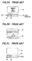
- a first conventional memory apparatus includes a memory cell array for storing data, a data register composed of a plurality of latch circuits, a transfer gate connected between the memory cell array and the data register, and a selector which is a shift register and is connected to the data register.
- the serial data is transferred to the memory cell array in parallel by the transfer gate, and is stored in the memory cell array.
- the serial data is transferred to the data register in parallel by the transfer gate, the serial data is latched therein by the corresponding latch circuits. Then, the latched serial data is transferred to the shift register for the selector, in which the serial data is shifted to be supplied to a following state.
- the structure is complicated because the shift register for the selector and the latch circuits for the data register require a number of elements to be used therein. Therefore, a cost of the memory apparatus is high.
- a second conventional memory apparatus which overcomes the above disadvantage of the first conventional memory apparatus includes a memory cell array, a data register which is a shift register including a plurality of flip-flop circuits, and a transfer gate connected between the memory cell array and the data register.
- the second conventional memory apparatus has been proposed in Japanese Patent Application No. 63-196708.
- the serial data is shifted therein in accordance with the clock signal. After that, when a last data bit of the serial data is stored in the data register, the serial data is transferred to the memory cell array in parallel by the transfer gate.
- the stored data is transferred to the data register in parallel by the transfer gate, the transferred data is shifted therein to an output side of the register, so that the serial data is supplied to a following stage.
- the second conventional memory device there is a disadvantage in that, if the number of data bits composing a serial data is smaller than the total shifting steps, each being of a flip-flop circuit, of the shift register, invalid data bits of the number equal to the difference between those of the serial data bits and the shifting steps are supplied from the data register at the beginning time when the serial data is read out, as explained in detail later.
- a memory apparatus includes: a memory cell array for storing a data of bits; a shift register for receiving an input serial data to be stored in the memory cell array and supplying an output serial data to be read from the memory cell array; a transfer gate which is positioned between the memory cell array and the shift register to transfer the data of bits in parallel therebetween; and a control circuit for controlling the shift register to shift the input serial data; wherein the control circuit controls the shift register to shift the input serial data until a first bit thereof reaches to a final step of the shift register, and then controls the transfer gate to transfer the input serial data in parallel to be stored in the memory cell array.
- the first conventional memory apparatus shown in Fig. 1 includes a memory cell array 10 for storing data, a data register 12 composed of a plurality of latch circuits, a transfer gate 14 connected between the memory cell array 10 and the data register 12, a selector 16 which is a shift register and is connected to the data register 12, and a control circuit 18 for controlling the memory cell array 10, the data register 12, the transfer gate 14 and the selector 16, respectively.
- the selector 16 is supplied with an input serial data SDI and supplies an output serial data SDO to a following stage.
- the control circuit 18 is supplied with a synchronous signal SYNC, a control signal WC for writing a serial data into the memory cell array 10 and a control signal RC for reading a serial data out of the memory cell array 10.
- the input serial data SDI supplied to the selector 16 is shifted therein by a clock signal.
- the serial data is then transferred to the data register 12, and is stored in corresponding latch circuit selected by the selector 16. After that, the serial data is transferred to the memory cell array 10 in parallel by the transfer gate 14, and is stored in the memory cell array 10.
- the stored data is transferred to the data register 12 in parallel by the transfer gate 14. Then, the transferred data is supplied to the selector 16, in which the data is shifted therein to be provided therefrom as a serial data to the following stage.
- the second conventional memory apparatus includes a memory cell array 10 for storing a data, a data register 20 which is a shift register, and a transfer gate 22 including transistors Q5 to Q8.
- the data register 20 includes flip-flops F1 to F5 connected in serial and transistors Q1 to Q4.
- the data register 20 is supplied with an input serial data SDI under the control of a clock signal CLK, and supplies an output serial data SDO to a following stage.
- the transfer gate 22 is supplied with a control signal TG to transfer a serial data between the memory cell array 10 and the data register 20.
- the control signal TG is applied through an inverter INV to gates of the transistors Q1 to Q4, and directly to gates of the transistors Q5 to Q8.
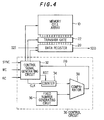
- the memory apparatus includes a memory cell array 10 for storing a data, a data register 20 which is a shift register, a transfer gate 22 connected between the memory cell array 10 and the data register 20, and a control circuit 30 for controlling the memory cell array 10, the data register 20 and the transfer gate 22, respectively.
- the control circuit 30 includes a control signal generating circuit 32, a counter 34 controlled to be supplied with a clock signal CLK and a reset signal RST by the control signal generating circuit 32, a fixed number generating circuit 36 which generates a number data corresponding to the number of flip-flops (not shown) composing the data register 20, and a comparator 38 connected at inputs to the counter 34 and the fixed number generating circuit 36 and at an output to the control signal generating circuit 32.
- the comparator 38 compares two signals supplied from the counter 34 and the fixed number generating circuit 36, and supplies an equal signal EQ when the counter output becomes equal to the fixed number.
- the control signal generating circuit 32 is supplied with a synchronous signal SYNC, a writing signal WC and a reading signal RC.
- the equal signal EQ is generated in the comparator 38 to be supplied to the control signal generating circuit 32.
- the serial data is stopped shifting, and the serial data is transferred to the memory cell array 10 in parallel by the transfer gate 22 as shown in Fig. 6C.
- the counter 34 is reset to be zero at the time t4 by the reset signal RST of a high level.
- the reading control signal RC is supplied to the control signal generating circuit 32
- the stored data is transferred from the memory cell array 10 to the data register 20 in parallel by the transfer gate 22 as shown in Fig. 6D.
- the serial data is supplied from the data register 20 bit by bit in the order of the first bit B F to the last bit B L to the following stage.
- the number of bits composing a serial data is smaller than that of flip-flops (not shown) composing the data register 20, an effective data bit is supplied instantly at the beginning time when the serial data is read out, because the serial data is written into the memory cell array 10 under a state thet the first bit B F reaches to the end step of the data register 20.
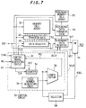
- a memory apparatus further includes a redundant memory cell array 50 for storing a redundant data, a redundant data register 52, a redundant data transfer gate 54 connected between the redundant memory cell array 50 and the redundant data register, a switching circuit 56 connected at inputs to outputs of the data register 20 and the redundant data register 52, and a selector 58 connected at an input to an output of the counter 34 and at an output to the switching circuit 56.
- the redundant memory cell array 50 stores a data corresponding to a disabled memory cell of the memory cell array 10.
- the redundant data register 52 is supplied with an input serial data SDI to be stored by a clock signal DCLK, when a signal RCLK becomes high, and supplies a redundant data RDT to the switching circuit 56.
- the selector 58 compares the number of clock pulses CLK counted by the counter 34 and a predetermined number corresponding to the disabled memory cell of the memory cell array 10, and supplies signals RCLK and RSEL when the number of the clock pulses CLK becomes to the number determined in the selector 58.
- the switching circuit 56 supplies an output serial data SDO by selecting one of the redundant data RDT and a normal data NDT supplied from the data register 20 in accordance with the signal RSEL from the selector 58.
- the reading control signal RC supplied to the control signal generating circuit 32 becomes high at a time t3, the data stored in the normal memory cells of the memory cell array 10 are transferred to the data register 20 by the transfer gate 22.
- a redundant data stored in the redundant memory cell array 50 is transferred to the redundant data register 52 by the redundant data transfer gate 54.
- the normal data NDT is supplied to the switching circuit 56 to be transmitted therethrough as the output serial data SDO, when the signal RSEL is low to be supplied to the switching circuit 56 (times t3 to t B ).
- the signal RSEL becomes high to be supplied to the switching circuit 56 at the time t B .
- the redundant data RDT is transferred from the redundant data register 52 to the switching circuit 56 and is supplied therefrom as the serial data output SDO instead of the normal data NDT to a following stage.
- the signal RSEL becomes low again, the data is supplied from the data register 20 through the switching circuit 56 to the following stage. Then, the whole bits of the serial data SDO are obtained at the output of the switching circuit 56 at a time t4.
- the memory apparatus operates normally.
Landscapes
- Engineering & Computer Science (AREA)
- Microelectronics & Electronic Packaging (AREA)
- Computer Hardware Design (AREA)
- Dram (AREA)
- For Increasing The Reliability Of Semiconductor Memories (AREA)
Applications Claiming Priority (2)
| Application Number | Priority Date | Filing Date | Title |
|---|---|---|---|
| JP2282826A JP2596208B2 (ja) | 1990-10-19 | 1990-10-19 | メモリ装置 |
| JP282826/90 | 1990-10-19 |
Publications (3)
| Publication Number | Publication Date |
|---|---|
| EP0481494A2 true EP0481494A2 (fr) | 1992-04-22 |
| EP0481494A3 EP0481494A3 (fr) | 1994-12-14 |
| EP0481494B1 EP0481494B1 (fr) | 1997-09-03 |
Family
ID=17657585
Family Applications (1)
| Application Number | Title | Priority Date | Filing Date |
|---|---|---|---|
| EP91117760A Expired - Lifetime EP0481494B1 (fr) | 1990-10-19 | 1991-10-17 | Appareil de mémoire |
Country Status (5)
| Country | Link |
|---|---|
| US (1) | US5343439A (fr) |
| EP (1) | EP0481494B1 (fr) |
| JP (1) | JP2596208B2 (fr) |
| KR (1) | KR0138751B1 (fr) |
| DE (1) | DE69127527T2 (fr) |
Cited By (1)
| Publication number | Priority date | Publication date | Assignee | Title |
|---|---|---|---|---|
| EP2932506A4 (fr) * | 2012-12-11 | 2016-08-10 | Hewlett Packard Entpr Dev Lp | Opération de données dans un cycle de registres à décalage |
Families Citing this family (19)
| Publication number | Priority date | Publication date | Assignee | Title |
|---|---|---|---|---|
| KR940024597A (ko) * | 1993-04-10 | 1994-11-18 | 김광호 | 듀얼포트 메모리장치의 시리얼데이타 입력장치. |
| JPH0713898A (ja) * | 1993-06-29 | 1995-01-17 | Mitsubishi Electric Corp | 半導体集積回路装置 |
| JPH07182893A (ja) * | 1993-12-24 | 1995-07-21 | Mitsubishi Electric Corp | 半導体記憶装置 |
| US5559753A (en) * | 1995-01-25 | 1996-09-24 | Dell Usa, L.P. | Apparatus and method for preventing bus contention during power-up in a computer system with two or more DRAM banks |
| US5682496A (en) | 1995-02-10 | 1997-10-28 | Micron Quantum Devices, Inc. | Filtered serial event controlled command port for memory |
| US5627786A (en) * | 1995-02-10 | 1997-05-06 | Micron Quantum Devices, Inc. | Parallel processing redundancy scheme for faster access times and lower die area |
| US6108237A (en) | 1997-07-17 | 2000-08-22 | Micron Technology, Inc. | Fast-sensing amplifier for flash memory |
| US5610873A (en) * | 1996-03-21 | 1997-03-11 | National Science Council Of R.O.C. | Address generator for generating a plurality of addresses to be used in zig-zag scanning of contents of memory array |
| US6172935B1 (en) | 1997-04-25 | 2001-01-09 | Micron Technology, Inc. | Synchronous dynamic random access memory device |
| US6728799B1 (en) * | 2000-01-13 | 2004-04-27 | Hewlett-Packard Development Company, L.P. | Hybrid data I/O for memory applications |
| US6993105B1 (en) | 2000-05-09 | 2006-01-31 | Cypress Semiconductor Corp. | Linearized digital phase-locked loop |
| US6417698B1 (en) * | 2000-05-12 | 2002-07-09 | Cypress Semiconductor Corp. | Linearized digital phase-locked loop method |
| US6950484B1 (en) | 2000-05-12 | 2005-09-27 | Cypress Semiconductor Corp. | Linearized digital phase-locked loop method |
| US6535023B1 (en) | 2000-05-12 | 2003-03-18 | Cypress Semiconductor Corp. | Linearized digital phase-locked loop method |
| US6711226B1 (en) | 2000-05-12 | 2004-03-23 | Cypress Semiconductor Corp. | Linearized digital phase-locked loop |
| KR100598010B1 (ko) * | 2004-08-06 | 2006-07-06 | 삼성전자주식회사 | 클럭 분배기, 클럭 분배기를 포함한 시스템, 클럭 분배방법 및 클럭 분배를 이용한 데이터 읽기 및 쓰기 방법 |
| US7826581B1 (en) | 2004-10-05 | 2010-11-02 | Cypress Semiconductor Corporation | Linearized digital phase-locked loop method for maintaining end of packet time linearity |
| US8083723B2 (en) * | 2007-04-05 | 2011-12-27 | Stealth Therapeutics, Inc. | Stabilized elongate implantable vascular access device |
| US8717831B2 (en) | 2012-04-30 | 2014-05-06 | Hewlett-Packard Development Company, L.P. | Memory circuit |
Family Cites Families (8)
| Publication number | Priority date | Publication date | Assignee | Title |
|---|---|---|---|---|
| US4330852A (en) * | 1979-11-23 | 1982-05-18 | Texas Instruments Incorporated | Semiconductor read/write memory array having serial access |
| JPH0760594B2 (ja) * | 1987-06-25 | 1995-06-28 | 富士通株式会社 | 半導体記憶装置 |
| US5195055A (en) * | 1987-11-30 | 1993-03-16 | Mitsubishi Denki Kabushiki Kaisha | Serial data input circuit for the shifting-in of variable length data |
| JPH07107792B2 (ja) * | 1988-01-19 | 1995-11-15 | 株式会社東芝 | マルチポートメモリ |
| US4873671A (en) * | 1988-01-28 | 1989-10-10 | National Semiconductor Corporation | Sequential read access of serial memories with a user defined starting address |
| JPH01224993A (ja) * | 1988-03-04 | 1989-09-07 | Nec Corp | マルチポートメモリ |
| JPH0748316B2 (ja) * | 1988-05-30 | 1995-05-24 | 日本電気株式会社 | デュアルポートメモリ回路 |
| US5084839A (en) * | 1990-02-05 | 1992-01-28 | Harris Corporation | Variable length shift register |
-
1990
- 1990-10-19 JP JP2282826A patent/JP2596208B2/ja not_active Expired - Fee Related
-
1991
- 1991-10-17 EP EP91117760A patent/EP0481494B1/fr not_active Expired - Lifetime
- 1991-10-17 DE DE69127527T patent/DE69127527T2/de not_active Expired - Fee Related
- 1991-10-18 KR KR1019910018375A patent/KR0138751B1/ko not_active Expired - Fee Related
- 1991-10-18 US US07/779,087 patent/US5343439A/en not_active Expired - Fee Related
Cited By (1)
| Publication number | Priority date | Publication date | Assignee | Title |
|---|---|---|---|---|
| EP2932506A4 (fr) * | 2012-12-11 | 2016-08-10 | Hewlett Packard Entpr Dev Lp | Opération de données dans un cycle de registres à décalage |
Also Published As
| Publication number | Publication date |
|---|---|
| DE69127527T2 (de) | 1998-02-12 |
| EP0481494B1 (fr) | 1997-09-03 |
| JP2596208B2 (ja) | 1997-04-02 |
| DE69127527D1 (de) | 1997-10-09 |
| US5343439A (en) | 1994-08-30 |
| KR920008750A (ko) | 1992-05-28 |
| EP0481494A3 (fr) | 1994-12-14 |
| JPH04157692A (ja) | 1992-05-29 |
| KR0138751B1 (ko) | 1998-06-15 |
Similar Documents
| Publication | Publication Date | Title |
|---|---|---|
| US5343439A (en) | Memory apparatus | |
| US6738918B2 (en) | High speed data transfer synchronizing system and method | |
| US4825411A (en) | Dual-port memory with asynchronous control of serial data memory transfer | |
| US5555548A (en) | Method and apparatus for transferring data between a master unit and a plurality of slave units | |
| EP0218830A2 (fr) | Appareil de test de mémoire | |
| EP0438273A2 (fr) | Dispositif de mémoire à semi-conducteur à redondance de colonne | |
| KR910005585B1 (ko) | 동기식 반도체 기억 장치 | |
| DE19653114C2 (de) | Synchron-Halbleiterspeichervorrichtung, bei der ein Burstzähler gemeinsam für ein Datenschreiben und für ein Datenlesen verwendet wird | |
| KR100694440B1 (ko) | 반도체기억장치 | |
| EP0416513B1 (fr) | Dispositif de mémoire fifo | |
| US5033001A (en) | Dual mode memory read cycle time reduction system which generates read data clock signals from shifted and synchronized trigger signals | |
| US7295489B2 (en) | Method and circuit for writing double data rate (DDR) sampled data in a memory device | |
| KR100768455B1 (ko) | 반도체 장치 | |
| JPS6374187A (ja) | 先入れ先出しメモリ | |
| KR100253565B1 (ko) | 동기식 기억소자의 양방향 데이타 입출력 회로 및 그 제어방법 | |
| US5475455A (en) | Information recording device | |
| JP3711200B2 (ja) | 直接アクセスモードテスト制御回路を備える高速半導体メモリ装置及びそのテスト方法 | |
| US6442103B1 (en) | Synchronous SRAM device with late write function | |
| US5444658A (en) | Elastic store memory circuit | |
| JPH04233646A (ja) | データ転送インタフェースモジュール | |
| US5917832A (en) | Self-test circuit and method utilizing interlaced scanning for testing a semiconductor memory device | |
| US5394404A (en) | Flip-flop circuit having diagnostic function | |
| CN101120299B (zh) | 异步抖动减小技术 | |
| JP2702318B2 (ja) | セル位相乗換回路 | |
| JP2758736B2 (ja) | セル位相乗換回路 |
Legal Events
| Date | Code | Title | Description |
|---|---|---|---|
| PUAI | Public reference made under article 153(3) epc to a published international application that has entered the european phase |
Free format text: ORIGINAL CODE: 0009012 |
|
| 17P | Request for examination filed |
Effective date: 19911017 |
|
| AK | Designated contracting states |
Kind code of ref document: A2 Designated state(s): DE FR GB |
|
| PUAL | Search report despatched |
Free format text: ORIGINAL CODE: 0009013 |
|
| AK | Designated contracting states |
Kind code of ref document: A3 Designated state(s): DE FR GB |
|
| 17Q | First examination report despatched |
Effective date: 19960117 |
|
| GRAG | Despatch of communication of intention to grant |
Free format text: ORIGINAL CODE: EPIDOS AGRA |
|
| GRAH | Despatch of communication of intention to grant a patent |
Free format text: ORIGINAL CODE: EPIDOS IGRA |
|
| GRAH | Despatch of communication of intention to grant a patent |
Free format text: ORIGINAL CODE: EPIDOS IGRA |
|
| GRAA | (expected) grant |
Free format text: ORIGINAL CODE: 0009210 |
|
| AK | Designated contracting states |
Kind code of ref document: B1 Designated state(s): DE FR GB |
|
| REF | Corresponds to: |
Ref document number: 69127527 Country of ref document: DE Date of ref document: 19971009 |
|
| ET | Fr: translation filed | ||
| PLBE | No opposition filed within time limit |
Free format text: ORIGINAL CODE: 0009261 |
|
| STAA | Information on the status of an ep patent application or granted ep patent |
Free format text: STATUS: NO OPPOSITION FILED WITHIN TIME LIMIT |
|
| 26N | No opposition filed | ||
| PGFP | Annual fee paid to national office [announced via postgrant information from national office to epo] |
Ref country code: GB Payment date: 19981023 Year of fee payment: 8 |
|
| PGFP | Annual fee paid to national office [announced via postgrant information from national office to epo] |
Ref country code: FR Payment date: 19981030 Year of fee payment: 8 |
|
| PGFP | Annual fee paid to national office [announced via postgrant information from national office to epo] |
Ref country code: DE Payment date: 19981221 Year of fee payment: 8 |
|
| PG25 | Lapsed in a contracting state [announced via postgrant information from national office to epo] |
Ref country code: GB Free format text: LAPSE BECAUSE OF NON-PAYMENT OF DUE FEES Effective date: 19991017 |
|
| GBPC | Gb: european patent ceased through non-payment of renewal fee |
Effective date: 19991017 |
|
| PG25 | Lapsed in a contracting state [announced via postgrant information from national office to epo] |
Ref country code: FR Free format text: LAPSE BECAUSE OF NON-PAYMENT OF DUE FEES Effective date: 20000630 |
|
| PG25 | Lapsed in a contracting state [announced via postgrant information from national office to epo] |
Ref country code: DE Free format text: LAPSE BECAUSE OF NON-PAYMENT OF DUE FEES Effective date: 20000801 |
|
| REG | Reference to a national code |
Ref country code: FR Ref legal event code: ST |