EP0481827A2 - Filtres colorés - Google Patents
Filtres colorés Download PDFInfo
- Publication number
- EP0481827A2 EP0481827A2 EP91309703A EP91309703A EP0481827A2 EP 0481827 A2 EP0481827 A2 EP 0481827A2 EP 91309703 A EP91309703 A EP 91309703A EP 91309703 A EP91309703 A EP 91309703A EP 0481827 A2 EP0481827 A2 EP 0481827A2
- Authority
- EP
- European Patent Office
- Prior art keywords
- polyamic acid
- black matrix
- color filter
- photo
- glass substrate
- Prior art date
- Legal status (The legal status is an assumption and is not a legal conclusion. Google has not performed a legal analysis and makes no representation as to the accuracy of the status listed.)
- Granted
Links
Images
Classifications
-
- G—PHYSICS
- G02—OPTICS
- G02F—OPTICAL DEVICES OR ARRANGEMENTS FOR THE CONTROL OF LIGHT BY MODIFICATION OF THE OPTICAL PROPERTIES OF THE MEDIA OF THE ELEMENTS INVOLVED THEREIN; NON-LINEAR OPTICS; FREQUENCY-CHANGING OF LIGHT; OPTICAL LOGIC ELEMENTS; OPTICAL ANALOGUE/DIGITAL CONVERTERS
- G02F1/00—Devices or arrangements for the control of the intensity, colour, phase, polarisation or direction of light arriving from an independent light source, e.g. switching, gating or modulating; Non-linear optics
- G02F1/01—Devices or arrangements for the control of the intensity, colour, phase, polarisation or direction of light arriving from an independent light source, e.g. switching, gating or modulating; Non-linear optics for the control of the intensity, phase, polarisation or colour
- G02F1/13—Devices or arrangements for the control of the intensity, colour, phase, polarisation or direction of light arriving from an independent light source, e.g. switching, gating or modulating; Non-linear optics for the control of the intensity, phase, polarisation or colour based on liquid crystals, e.g. single liquid crystal display cells
- G02F1/133—Constructional arrangements; Operation of liquid crystal cells; Circuit arrangements
- G02F1/1333—Constructional arrangements; Manufacturing methods
- G02F1/1335—Structural association of cells with optical devices, e.g. polarisers or reflectors
-
- G—PHYSICS
- G02—OPTICS
- G02F—OPTICAL DEVICES OR ARRANGEMENTS FOR THE CONTROL OF LIGHT BY MODIFICATION OF THE OPTICAL PROPERTIES OF THE MEDIA OF THE ELEMENTS INVOLVED THEREIN; NON-LINEAR OPTICS; FREQUENCY-CHANGING OF LIGHT; OPTICAL LOGIC ELEMENTS; OPTICAL ANALOGUE/DIGITAL CONVERTERS
- G02F1/00—Devices or arrangements for the control of the intensity, colour, phase, polarisation or direction of light arriving from an independent light source, e.g. switching, gating or modulating; Non-linear optics
- G02F1/01—Devices or arrangements for the control of the intensity, colour, phase, polarisation or direction of light arriving from an independent light source, e.g. switching, gating or modulating; Non-linear optics for the control of the intensity, phase, polarisation or colour
- G02F1/13—Devices or arrangements for the control of the intensity, colour, phase, polarisation or direction of light arriving from an independent light source, e.g. switching, gating or modulating; Non-linear optics for the control of the intensity, phase, polarisation or colour based on liquid crystals, e.g. single liquid crystal display cells
- G02F1/133—Constructional arrangements; Operation of liquid crystal cells; Circuit arrangements
- G02F1/136—Liquid crystal cells structurally associated with a semi-conducting layer or substrate, e.g. cells forming part of an integrated circuit
- G02F1/1362—Active matrix addressed cells
- G02F1/136209—Light shielding layers, e.g. black matrix, incorporated in the active matrix substrate, e.g. structurally associated with the switching element
-
- G—PHYSICS
- G03—PHOTOGRAPHY; CINEMATOGRAPHY; ANALOGOUS TECHNIQUES USING WAVES OTHER THAN OPTICAL WAVES; ELECTROGRAPHY; HOLOGRAPHY
- G03F—PHOTOMECHANICAL PRODUCTION OF TEXTURED OR PATTERNED SURFACES, e.g. FOR PRINTING, FOR PROCESSING OF SEMICONDUCTOR DEVICES; MATERIALS THEREFOR; ORIGINALS THEREFOR; APPARATUS SPECIALLY ADAPTED THEREFOR
- G03F7/00—Photomechanical, e.g. photolithographic, production of textured or patterned surfaces, e.g. printing surfaces; Materials therefor, e.g. comprising photoresists; Apparatus specially adapted therefor
- G03F7/004—Photosensitive materials
- G03F7/075—Silicon-containing compounds
- G03F7/0751—Silicon-containing compounds used as adhesion-promoting additives or as means to improve adhesion
-
- G—PHYSICS
- G02—OPTICS
- G02F—OPTICAL DEVICES OR ARRANGEMENTS FOR THE CONTROL OF LIGHT BY MODIFICATION OF THE OPTICAL PROPERTIES OF THE MEDIA OF THE ELEMENTS INVOLVED THEREIN; NON-LINEAR OPTICS; FREQUENCY-CHANGING OF LIGHT; OPTICAL LOGIC ELEMENTS; OPTICAL ANALOGUE/DIGITAL CONVERTERS
- G02F1/00—Devices or arrangements for the control of the intensity, colour, phase, polarisation or direction of light arriving from an independent light source, e.g. switching, gating or modulating; Non-linear optics
- G02F1/01—Devices or arrangements for the control of the intensity, colour, phase, polarisation or direction of light arriving from an independent light source, e.g. switching, gating or modulating; Non-linear optics for the control of the intensity, phase, polarisation or colour
- G02F1/13—Devices or arrangements for the control of the intensity, colour, phase, polarisation or direction of light arriving from an independent light source, e.g. switching, gating or modulating; Non-linear optics for the control of the intensity, phase, polarisation or colour based on liquid crystals, e.g. single liquid crystal display cells
- G02F1/133—Constructional arrangements; Operation of liquid crystal cells; Circuit arrangements
- G02F1/1333—Constructional arrangements; Manufacturing methods
- G02F1/1335—Structural association of cells with optical devices, e.g. polarisers or reflectors
- G02F1/133509—Filters, e.g. light shielding masks
- G02F1/133514—Colour filters
- G02F1/133516—Methods for their manufacture, e.g. printing, electro-deposition or photolithography
Definitions
- the present invention relates to a color filter used for color liquid crystal display unit, and in particular to a color filter having special features in black matrix.
- a liquid crystal display unit In a liquid crystal display unit, at least two transparent substrates made of the arterial such as glass having transparent electrodes are provided face to face to each other with spacings of 1 to 10 ⁇ m, and liquid crystal substance is sealed therebetween and the liquid crystals are oriented in a certain direction by applying voltage across the electrodes so that transparent and non-transparent portions are formed to display the image.
- a color liquid crystal display unit three-color filters for red (R), green (G) and blue (B) corresponding to three primary colors of light are furnished on one of transparent electrode substrates. By adjusting the voltage applied on the transparent electrode, the transmission of liquid crystal light is controlled.
- color display is accomplished by developing colors through the addition of 3 primary colors.
- the layers colored with the colors of R, G and B of a color filter are forced on a substrate where black matrix is provided for defining the boundary of the colors.
- Black matrix defines three primary colors of R, G and B of the color layers, and it also shields the light for the electrodes for driving of liquid crystal or transistor such as TFT on the substrate placed face-to-face to the color filter.
- the black matrix formed on the color filter is usually formed by thin film of metals such as chromium, nickel, aluminum, etc.
- the black matrix thin film of these metals is placed on glass substrate by the methods such as sputtering, vacuum evaporation, etc. Then, photo-resist patterns are formed by the technique of photolithography, and the pattern is formed by etching metal thin film using photo-resist pattern as the etching mask.
- black matrix made of metal thin film is formed by the methods such as sputtering, vacuum evaporation, etc., the cost for forming film is expensive. Because metal thin film has metallic luster, the reflected light from metal chromium thin film is increased in case the light entering the display unit from outside is strong, and this results in the deterioration of display quality in a transmission type display unit such as liquid crystal display unit.
- chromium thin film For the purpose of decreasing the reflectivity of metal chromium, it is proposed to form chromium thin film after a film of low reflectivity such as chromium oxide is placed on glass substrate before metal chromium thin film is formed.
- a film of low reflectivity such as chromium oxide is placed on glass substrate before metal chromium thin film is formed.
- this is not very desirable because more processes are required and the manufacturing cost is increased.
- the present inventors have proposed the following manufacturing method in the Japanese Patent Application which describes a color filter having black matrix made of polyimide type resin with dispersed light shielding material such as carbon black as the black matrix with low reflectivity and low manufacturing cost, and which also discloses a method for manufacturing such color filter.
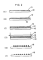
- Fig. 2 shows a cross-sectional view of color filter
- carbon black, metal oxides such as triiron tetraoxide or mixture of these substances are dispersed in polyamic acid solution, and this is coated on the glass substrate 10 by roll coating method or spin coating method to form the coated layer 12 as shown in Fig. 2 (B).
- Fig. 2 (C) After polyamic acid is coated, pre-baking is performed as shown in Fig. 2 (C). Then, photo-resist is coated on the coated layer of polyamic acid compositions to form a photo-resist layer 13. The photo-resist layer is exposed to light using a predetermined photo mask 14 as shown in Fig. 2 (D) and the image is developed. Thus, the desired pattern is formed on the photo-resist layer.
- the coated layer of polyamic acid is etched according to the pattern of the photo resist layer, and the photo-resist layer is detached as given in Fig. 2 (F).
- black matrix is also damaged as it is an organic substance located in lower layer of the photo-resist layer. For this reason, it is practiced to selectively dissolve and detach only the photoresist layer using various types of organic solvents.
- organic solvents such as acetone, methylethylketone, etc., alcoholic type organic solvents such as methanol, ethanol, etc. cellosolve type organic solvents such as ethyl cellosolve, cellosolve acetate type solvents such as ethyl cellosolve acetate, ester type organic solvents such as butyl acetate, or glycol type organic solvents.
- aminosilane type coupling agent such as ⁇ -(2-aminoethyl)-aminopropyl-trimethoxysilane, ⁇ -aminopropyltriethoxysilane, etc. having high affinity with silicon, which is a component of glass, has been used.
- the object of the present invention is to offer a compound, which can form black matrix having high adhesive strength to glass substrate, and it is characterized in that the adhesive strength of polyimide layer is increased either by coating the substrate with a compound consisting of silane coupling agent having epoxy group mixed with the mixture containing a polyimide precursor composed of polyamic acid, or by coating the mixture containing a polyimide precursor on a layer of epoxy type silane coupling agent formed on the substrate.
- epoxysilane usable for the purpose of this invention ⁇ -glycidoxypropyltrimethoxysilane, ⁇ -glycidoxypropylmethyldiethoxysilane, ⁇ -(3,4-epoxycyclohexyl)-ethyltrimethoxysilane, etc. can be used.
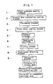
- Fig. 1 is a drawing for explaining the manufacturing process of such color filter.
- the substrate made from Corning 7059 or borosilicate glass with lower thermal expansion coefficient or soda lime glass are used, and organic substances attached on glass substrate surface are removed by organic solvent, acid, alkali, water, etc. in the washing process 1 of glass substrate.
- the glass substrate is coated with the solution, in which light shielding material for preventing the transmission of light is dispersed in the solution of polyamic acid, easily imidized by heating, by means of roll coating method or spin coating method.
- polyimide precursor such as PIQ/PIX series (Hitachi Chemical Co., Ltd.), Semico Fine SP series (Toray Industries, Inc.), Pymel series (Asahi Chemical Industries Co., ltd.), Pyralin series (DuPont), etc. are used.
- pigments such as carbon black, triiron tetraoxide, etc. are dispersed.
- the light shielding material is dispersed by stirring the solution, or by ball mill method, or 3-roll method. If a small quantity of surface active agent is added, the dispersion of light shielding material can be stabilized.
- the particle used as light shielding material is 1 ⁇ m or less in size to attain the stability of the dispersed particles.
- silane coupling agent having epoxy group is mixed to the solution of polyamic acid.
- Silane coupling agent with epoxy group is added by 0.005% to 0.5% in weight to polyamic acid solution.
- the adhesive strength of black matrix is improved less.
- it is mixed by 0.5% or more, no change is seen in the mixed compound, but the film of polyamic acid cannot be removed completely even if it is attempted to remove it by etching through the mask of the photo-resist pattern formed on the coated polyamic acid film. Thus, it should be mixed by 0.5% or more.
- the film thickness of polyamic acid composition thus formed varies according to the optical shielding property of polyamic acid, in which shielding material is dispersed, the film with thickness of 0.5 to 2.0 ⁇ m is formed. And after polyamic acid solution with dispersed shielding material is coated, pre-baking treatment is performed in the pre-baking process 3 by heating at 130°C to 150°C for 30 minutes.
- a predetermined pattern is formed on the film coated with polyamic acid.
- photo-resist is coated on the polyamic acid coated film in the photo-resist coating process 4, and after pre-baking it on a heat plate or in an oven heated at 90°C to 100°C, the pattern is formed by the technique of photolithography.
- the photo-resist of both positive and negative types can be used.
- novolak type photo-resist which is widely used as positive type photo-resists because, after exposure to light using photomask, alkali solution such as sodium hydroxide, tetramethyl ammonium, etc. can be used for development.
- alkali solution such as sodium hydroxide, tetramethyl ammonium, etc.
- the exposed portion of photo-resist is removed by alkali solution and polyamic acid is also removed at the same time.
- the photo-resist with the predetermined pattern is exposed to light in the exposure process 5 using ultra-high voltage mercury lamp as light source, and the pattern is then developed in the developing process 6.
- photo-resist detaching process 8 photo-resist is detached, which remains on the film coated with polyamic acid composition, formed in the predetermined pattern on glass substrate.
- photo-resist can be easily detached by the following organic solvents: ketone type organic solvents such as acetone, methylethylketone, etc. alcohol type solvents such as methanol, ethanol, etc., cellosolve type solvent such as ethyl cellosolve, or ester type solvents such as butyl acetate, or glycol type organic solvents.
- ketone type organic solvents such as acetone, methylethylketone, etc.
- alcohol type solvents such as methanol, ethanol, etc.
- cellosolve type solvent such as ethyl cellosolve
- ester type solvents such as butyl acetate
- glycol type organic solvents such as butyl acetate, or glycol type organic solvents.
- glycol ethers such as ethyleneglycol monobutyl ether, diethyleneglycol diethyl ether, diethyleneglycol monoether acetate, dipropyleneglycol monomethyl ether, etc. because these have ignition point of 70°C or above and are compatible with water, are easier to handle and water can be used also for the washing process of residue after the detachment process. Thus, the process can be simplified.
- Some organic solvents may cause damage such as cracking or dissolving to the polyamic acid coated film thus pre-baked but the detachment solution using glycol ether does not cause such damage.
- composition containing polyamic acid after detaching photo resist is turned to polyimide in the imidization process 9 by heating polyamic acid to 250°C or more.
- a colored layer is provided by photolithography or printing method.
- Transparent protective film is formed on the colored layer, and transparent electrode layer with the predetermined pattern is formed on the transparent protective film.
- a color filter is manufactured.
- black matrix with high bonding strength can be obtained without the pre-treatment process for glass substrate, i.e. without coating process and drying process for silane coupling agent.
- Epoxy type silane coupling agent is coated on glass substrate to form a layer. After coating polyimide precursor composition on it, the pattern is formed, and polyimide precursor is imidized.
- composition containing polyamic acid after detaching photo-resist is turned to polyimide in the imidization process 9 by heating polyamic acid at 250°C or more.
- a glass substrate (Corning 7059) with thickness of 1.1 mm is used as substrate after throughly washing.
- polyimide precursor 14% solution of Pyralin PI-2545 (DuPont) commercially available is used as polyamic acid.
- polyamic acid Converted to 100%
- carbon black is added to one part of polyamic acid (converted to 100%).
- ⁇ -butyl lactone is added to the dispersion solution thus obtained to adjust viscosity.
- ⁇ -glycidoxy-propyltrimethoxysilane Toray Silicone Co., Ltd.; SH6020
- SH6020 ⁇ -glycidoxy-propyltrimethoxysilane
- This solution was coated on glass substrate in a thickness of 1.5 ⁇ m by spin coating and was pre-baked by heating to 130°C on a hot plate to remove organic solvent.
- OFPR-800 Tokyo Ohka Industry Co., Ltd.
- a hot plate heated to 90°C On the polyamic acid coated film, OFPR-800 (Tokyo Ohka Industry Co., Ltd.) was coated as positive type resist, and it was pre-baked on a hot plate heated to 90°C.
- the coated film formed on the substrate 1 was exposed to light irradiated from 2.0 kW ultra-high voltage mercury lamp for 10 seconds through a photo mask. Then, the exposed portion of photo resist was removed, using NMD-3 (Tokyo Ohka Industry Co., Ltd.) as developing solution, and polyamic acid etching was performed at the same time.
- NMD-3 Tokyo Ohka Industry Co., Ltd.
- the color filter was immersed for 45 seconds in diethyleneglycol monobutyl ether. After the photo resist on the polyamic acid coated film was detached, it was washed with water. When the black matrix was examined under microscope (x 400), no defect was found such as cracking, narrowed line width, etc.
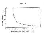
- the minimum line width of the pattern of formable polyimide depends upon the adding quantity of epoxy silane added to polyamic acid as shown in Fig. 3. Namely, if the adding quantity of epoxy silane is too low, sufficient bonding strength is not obtained between polyamic acid and glass substrate, and fine pattern is separated from the glass substrate during polyamic acid etching or during rinsing. Therefore, to form the pattern of 10 ⁇ m or less, which is required as black matrix layer for color filter for liquid crystal display unit, it is necessary to add epoxy silane by 0.05 wt % or more.
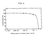
- Fig. 4 summarizes the results of the measurement by the light of 450 nm, showing the relationship between the adding quantity of epoxy silane and the light transmittance of the transparent portion, where black matrix removed by etching is not formed.
- the polyamic acid composition containing epoxy silane by 0.2 wt % or more is difficult to etch, and sufficient transmission is not obtained because black matrix thin film containing light shielding material remains on the portion, which is originally to be removed.
- epoxy silane is added by 0.05 wt % to 0.1 wt %.
- red, green and blue pigments are dispersed on photosensitive resin by the composition ratio as shown in Table 1 to prepare colored photosensitive resins in red, green and blue.
- the red photosensitive resin was coated in a thickness of 1.2 ⁇ m. Then, it was dried in an oven kept at 70°C for 30 minutes, and it was exposed to light using a mercury lamp. Spray development with water was performed for 1 minute, and red relief image was formed in an area where red pixel should be formed. Further, it was heated and hardened at 150°C for 30 minutes.
- green relief image was formed on an area where green pixel should be formed, and blue relief image was formed in an area where blue pixel should be formed.
- colored layers were prepared.
- light curing mixture was prepared by mixing 35 weight parts of o-cresol-novolak epoxy acrylate (molecular weight 1500 - 2000) as light curing acrylate oligomer and 15 weight parts of cresol novolak type epoxy resin, and by mixing 50 weight parts of dipentaerythritol hexacrylate (Nippon Kayaku Co., Ltd.; DPHA) as multifunctional polymeric monomer. Further, 2 weight parts of Ilgacure (Ciba Geigy) was added as polymerization initiator, and 2 weight parts of UVE1014(General Electric) was added as epoxy curing agent. This mixture is dissolved in 200 weight parts of ethyl cellosolve acetate.
- ITO film composite film of indium oxide and tin oxide
- a color filter was manufactured by the same procedure as in the Example 1, except that the photo resist on the coated film of polyamic acid was detached by immersing in diethyleneglycol for 90 seconds. When the black matrix was examined under microscope (x 400), cracking was seen at the crossings of grids.
Landscapes
- Physics & Mathematics (AREA)
- Nonlinear Science (AREA)
- General Physics & Mathematics (AREA)
- Mathematical Physics (AREA)
- Chemical & Material Sciences (AREA)
- Crystallography & Structural Chemistry (AREA)
- Optics & Photonics (AREA)
- Engineering & Computer Science (AREA)
- Microelectronics & Electronic Packaging (AREA)
- Optical Filters (AREA)
- Liquid Crystal (AREA)
- Compositions Of Macromolecular Compounds (AREA)
Applications Claiming Priority (2)
| Application Number | Priority Date | Filing Date | Title |
|---|---|---|---|
| JP2280753A JPH04156402A (ja) | 1990-10-19 | 1990-10-19 | カラーフィルター |
| JP280753/90 | 1990-10-19 |
Publications (3)
| Publication Number | Publication Date |
|---|---|
| EP0481827A2 true EP0481827A2 (fr) | 1992-04-22 |
| EP0481827A3 EP0481827A3 (en) | 1992-09-30 |
| EP0481827B1 EP0481827B1 (fr) | 1996-07-31 |
Family
ID=17629476
Family Applications (1)
| Application Number | Title | Priority Date | Filing Date |
|---|---|---|---|
| EP91309703A Expired - Lifetime EP0481827B1 (fr) | 1990-10-19 | 1991-10-21 | Filtres colorés |
Country Status (5)
| Country | Link |
|---|---|
| US (1) | US5251071A (fr) |
| EP (1) | EP0481827B1 (fr) |
| JP (1) | JPH04156402A (fr) |
| KR (1) | KR920008527A (fr) |
| DE (1) | DE69121161T2 (fr) |
Cited By (4)
| Publication number | Priority date | Publication date | Assignee | Title |
|---|---|---|---|---|
| EP0605685A4 (fr) * | 1992-06-01 | 1994-11-02 | Advanced Tech Incubator | Element agissant sur la lumiere pour des systemes optiques a haute resolution et procede de fabrication. |
| EP0740183A1 (fr) * | 1995-04-24 | 1996-10-30 | DAINICHI SEIKA COLOR & CHEMICALS MFG. CO. LTD. | Composition pour une matrice noire, procédé de fabrication d'une telle matrice et article comprenant une telle matrice |
| EP0867748A3 (fr) * | 1997-03-27 | 2000-09-06 | Canon Kabushiki Kaisha | Filtre coloré, sa méthode de fabrication et panneau d'affichage à cristaux liquides l'utilisant |
| CN103838083A (zh) * | 2012-11-20 | 2014-06-04 | 奇美实业股份有限公司 | 感光性树脂组合物、其所形成的彩色滤光片及其液晶显示元件 |
Families Citing this family (27)
| Publication number | Priority date | Publication date | Assignee | Title |
|---|---|---|---|---|
| JP2794499B2 (ja) * | 1991-03-26 | 1998-09-03 | 株式会社半導体エネルギー研究所 | 半導体装置の作製方法 |
| US5414442A (en) * | 1991-06-14 | 1995-05-09 | Semiconductor Energy Laboratory Co., Ltd. | Electro-optical device and method of driving the same |
| US6975296B1 (en) | 1991-06-14 | 2005-12-13 | Semiconductor Energy Laboratory Co., Ltd. | Electro-optical device and method of driving the same |
| US6778231B1 (en) | 1991-06-14 | 2004-08-17 | Semiconductor Energy Laboratory Co., Ltd. | Electro-optical display device |
| US6005651A (en) * | 1992-08-04 | 1999-12-21 | Matsushita Electric Industrial Co., Ltd. | Display panel and projection display system with use of display panel |
| JPH06167705A (ja) * | 1992-11-30 | 1994-06-14 | Sanyo Electric Co Ltd | 単板式液晶プロジェクター |
| KR100200199B1 (ko) * | 1994-08-02 | 1999-06-15 | 사또 아끼오 | 광학필터용 폴리이미드수지조성물 |
| TW425484B (en) * | 1995-04-28 | 2001-03-11 | Toray Industries | A resin black matrix for liquid crystal display device |
| KR0182877B1 (ko) * | 1995-11-25 | 1999-05-01 | 구자홍 | 액정표시장치의 구조 및 그 제조방법 |
| EP0794452B1 (fr) * | 1996-03-08 | 2007-03-21 | Canon Kabushiki Kaisha | Dispositif d'affichage et son procédé de fabrication |
| KR100209277B1 (ko) * | 1996-04-25 | 1999-07-15 | 구자홍 | 박막트랜지스터 어레이 기판 및 그 제조방법 |
| JP3549176B2 (ja) * | 1997-07-28 | 2004-08-04 | 株式会社東芝 | 液晶表示装置、およびカラーフィルタ基板の製造方法 |
| KR100870020B1 (ko) * | 2002-10-04 | 2008-11-21 | 삼성전자주식회사 | 용해 특성을 조절하는 감광성 수지 조성물 및 이를 이용한이층 구조의 패턴 형성 방법 |
| EP2139953B1 (fr) | 2007-04-24 | 2014-04-16 | Cabot Corporation | Noir de carbone à faible structure et procédé de fabrication de celui-ci |
| US11497681B2 (en) | 2012-02-28 | 2022-11-15 | Corning Incorporated | Glass articles with low-friction coatings |
| CN107540242B (zh) | 2012-02-28 | 2020-11-20 | 康宁股份有限公司 | 具有低摩擦涂层的玻璃制品 |
| US10737973B2 (en) | 2012-02-28 | 2020-08-11 | Corning Incorporated | Pharmaceutical glass coating for achieving particle reduction |
| US10273048B2 (en) | 2012-06-07 | 2019-04-30 | Corning Incorporated | Delamination resistant glass containers with heat-tolerant coatings |
| US9034442B2 (en) | 2012-11-30 | 2015-05-19 | Corning Incorporated | Strengthened borosilicate glass containers with improved damage tolerance |
| US10117806B2 (en) | 2012-11-30 | 2018-11-06 | Corning Incorporated | Strengthened glass containers resistant to delamination and damage |
| RU2691189C2 (ru) | 2014-09-05 | 2019-06-11 | Корнинг Инкорпорейтед | Стеклянные изделия и способы повышения надежности стеклянных изделий |
| EP3206998B1 (fr) | 2014-11-26 | 2021-09-08 | Corning Incorporated | Procédés pour la production de récipients en verre renforcé et durable |
| EP3150564B1 (fr) | 2015-09-30 | 2018-12-05 | Corning Incorporated | Compositions chimiques à base de polyimide-siloxane halogéné et articles en verre avec des revêtements à faible frottement en polylmide-siloxane halogéné |
| US20170121058A1 (en) | 2015-10-30 | 2017-05-04 | Corning Incorporated | Glass articles with mixed polymer and metal oxide coatings |
| CN112445019A (zh) * | 2019-09-05 | 2021-03-05 | 咸阳彩虹光电科技有限公司 | 一种功能基板、液晶显示面板及显示器 |
| WO2022051645A2 (fr) | 2020-09-04 | 2022-03-10 | Corning Incorporated | Emballages pharmaceutiques revêtus bloquant la lumière ultraviolette |
| CN113161329A (zh) * | 2021-03-12 | 2021-07-23 | 华南理工大学 | 具有高光色性能的rgb光源器件及其制备方法、显示屏 |
Family Cites Families (5)
| Publication number | Priority date | Publication date | Assignee | Title |
|---|---|---|---|---|
| SE366505B (fr) * | 1972-03-03 | 1974-04-29 | Volvo Ab | |
| WO1986004688A1 (fr) * | 1985-02-05 | 1986-08-14 | Kyodo Printing Co., Ltd. | Filtre colore et son procede de production |
| JPH0721562B2 (ja) * | 1987-05-14 | 1995-03-08 | 凸版印刷株式会社 | カラ−フイルタ |
| US4934791A (en) * | 1987-12-09 | 1990-06-19 | Matsushita Electric Industrial Co., Ltd. | Color filter |
| EP0326112B1 (fr) * | 1988-01-29 | 1994-09-14 | Toppan Printing Co., Ltd. | Structures d'électrodes pour dispositif d'affichage et son procédé de production |
-
1990
- 1990-10-19 JP JP2280753A patent/JPH04156402A/ja active Pending
-
1991
- 1991-10-18 KR KR1019910018445A patent/KR920008527A/ko not_active Ceased
- 1991-10-18 US US07/779,353 patent/US5251071A/en not_active Expired - Lifetime
- 1991-10-21 DE DE69121161T patent/DE69121161T2/de not_active Expired - Lifetime
- 1991-10-21 EP EP91309703A patent/EP0481827B1/fr not_active Expired - Lifetime
Cited By (6)
| Publication number | Priority date | Publication date | Assignee | Title |
|---|---|---|---|---|
| EP0605685A4 (fr) * | 1992-06-01 | 1994-11-02 | Advanced Tech Incubator | Element agissant sur la lumiere pour des systemes optiques a haute resolution et procede de fabrication. |
| EP0740183A1 (fr) * | 1995-04-24 | 1996-10-30 | DAINICHI SEIKA COLOR & CHEMICALS MFG. CO. LTD. | Composition pour une matrice noire, procédé de fabrication d'une telle matrice et article comprenant une telle matrice |
| AU703135B2 (en) * | 1995-04-24 | 1999-03-18 | Dainichiseika Color & Chemicals Mfg. Co. Ltd. | Composition for black matrix, fabrication process of black matrix, and article provided with black matrix |
| EP0867748A3 (fr) * | 1997-03-27 | 2000-09-06 | Canon Kabushiki Kaisha | Filtre coloré, sa méthode de fabrication et panneau d'affichage à cristaux liquides l'utilisant |
| CN103838083A (zh) * | 2012-11-20 | 2014-06-04 | 奇美实业股份有限公司 | 感光性树脂组合物、其所形成的彩色滤光片及其液晶显示元件 |
| CN103838083B (zh) * | 2012-11-20 | 2017-01-04 | 奇美实业股份有限公司 | 感光性树脂组合物、其所形成的彩色滤光片及其液晶显示元件 |
Also Published As
| Publication number | Publication date |
|---|---|
| DE69121161D1 (de) | 1996-09-05 |
| DE69121161T2 (de) | 1997-03-06 |
| KR920008527A (ko) | 1992-05-28 |
| JPH04156402A (ja) | 1992-05-28 |
| US5251071A (en) | 1993-10-05 |
| EP0481827A3 (en) | 1992-09-30 |
| EP0481827B1 (fr) | 1996-07-31 |
Similar Documents
| Publication | Publication Date | Title |
|---|---|---|
| US5251071A (en) | Color filter | |
| KR100338428B1 (ko) | 차광층을가진기판의형성방법,차광층을가진기판,흑백표시박막트랜지스터(tft)어레이기판용대향전극기판및흑백표시액정디스플레이장치 | |
| KR100376156B1 (ko) | 액정표시소자용수지블랙매트릭스 | |
| KR100292634B1 (ko) | 안료분산형컬러필터용조성물 | |
| US5503952A (en) | Method for manufacture of color filter and liquid crystal display | |
| JP2575572B2 (ja) | アルカリ現像型感光性カラーフィルター用インク及びそれを用いたカラーフィルター | |
| JP3470352B2 (ja) | カラーフィルタ | |
| US5214541A (en) | Method for producing color filter | |
| JPH10142418A (ja) | カラーフィルター及び液晶表示装置の製造方法 | |
| JP3230794B2 (ja) | 高抵抗黒色感放射線性樹脂組成物及び黒色硬化膜並びにその黒色画像形成方法 | |
| JPH04190362A (ja) | 遮光膜およびその製造方法 | |
| JP4465752B2 (ja) | 電極基板および液晶表示装置 | |
| JP5540649B2 (ja) | カラーフィルター用赤色着色組成物、液晶表示装置用カラーフィルター基板、および液晶表示装置 | |
| JP2002145999A (ja) | 光重合性不飽和樹脂および該樹脂を含有する感光性樹脂組成物 | |
| US5399449A (en) | Method for producing color filter wherein the voltage used to electrodeposit the colored layers is decreased with each subsequent electrodeposition step | |
| US5721089A (en) | Photosensitive material, color filter and liquid crystal device having the color filter | |
| JP2000329926A (ja) | 顔料分散樹脂溶液組成物、その製造方法およびカラーフィルター | |
| JP2000199967A (ja) | 樹脂製ブラックマトリクスの製造方法、該ブラックマトリクスを用いたカラ―フィルタの製造方法、及び該製造方法で製造されたカラ―フィルタを用いた液晶素子 | |
| JP2002341128A (ja) | カラーフィルターおよび液晶表示素子の製造方法 | |
| JP2000199815A (ja) | カラ―フィルタおよびその製造方法 | |
| JPH085829A (ja) | 液晶表示素子用カラーフィルタ | |
| EP0636931A1 (fr) | Méthode pour fabriquer un substrat portant des films en forme de cadre et fenêtre sur sa surface | |
| JPH11242111A (ja) | カラーフィルタ保護膜用組成物、カラーフィルタ付き基板、その製法及び液晶表示素子 | |
| JP3992801B2 (ja) | カラーフィルタの製造方法 | |
| JP2003287614A (ja) | カラーフィルターの製造方法 |
Legal Events
| Date | Code | Title | Description |
|---|---|---|---|
| PUAI | Public reference made under article 153(3) epc to a published international application that has entered the european phase |
Free format text: ORIGINAL CODE: 0009012 |
|
| AK | Designated contracting states |
Kind code of ref document: A2 Designated state(s): DE FR GB NL |
|
| PUAL | Search report despatched |
Free format text: ORIGINAL CODE: 0009013 |
|
| AK | Designated contracting states |
Kind code of ref document: A3 Designated state(s): DE FR GB NL |
|
| 17P | Request for examination filed |
Effective date: 19921102 |
|
| 17Q | First examination report despatched |
Effective date: 19940930 |
|
| GRAH | Despatch of communication of intention to grant a patent |
Free format text: ORIGINAL CODE: EPIDOS IGRA |
|
| GRAH | Despatch of communication of intention to grant a patent |
Free format text: ORIGINAL CODE: EPIDOS IGRA |
|
| GRAA | (expected) grant |
Free format text: ORIGINAL CODE: 0009210 |
|
| AK | Designated contracting states |
Kind code of ref document: B1 Designated state(s): DE FR GB NL |
|
| ET | Fr: translation filed | ||
| REF | Corresponds to: |
Ref document number: 69121161 Country of ref document: DE Date of ref document: 19960905 |
|
| PLBE | No opposition filed within time limit |
Free format text: ORIGINAL CODE: 0009261 |
|
| STAA | Information on the status of an ep patent application or granted ep patent |
Free format text: STATUS: NO OPPOSITION FILED WITHIN TIME LIMIT |
|
| 26N | No opposition filed | ||
| REG | Reference to a national code |
Ref country code: GB Ref legal event code: IF02 |
|
| PGFP | Annual fee paid to national office [announced via postgrant information from national office to epo] |
Ref country code: GB Payment date: 20090922 Year of fee payment: 19 |
|
| PGFP | Annual fee paid to national office [announced via postgrant information from national office to epo] |
Ref country code: DE Payment date: 20091123 Year of fee payment: 19 |
|
| PGFP | Annual fee paid to national office [announced via postgrant information from national office to epo] |
Ref country code: NL Payment date: 20090924 Year of fee payment: 19 |
|
| REG | Reference to a national code |
Ref country code: NL Ref legal event code: V1 Effective date: 20110501 |
|
| GBPC | Gb: european patent ceased through non-payment of renewal fee |
Effective date: 20101021 |
|
| PG25 | Lapsed in a contracting state [announced via postgrant information from national office to epo] |
Ref country code: FR Free format text: LAPSE BECAUSE OF NON-PAYMENT OF DUE FEES Effective date: 20101102 |
|
| REG | Reference to a national code |
Ref country code: FR Ref legal event code: ST Effective date: 20110630 |
|
| REG | Reference to a national code |
Ref country code: DE Ref legal event code: R119 Ref document number: 69121161 Country of ref document: DE Effective date: 20110502 |
|
| PG25 | Lapsed in a contracting state [announced via postgrant information from national office to epo] |
Ref country code: GB Free format text: LAPSE BECAUSE OF NON-PAYMENT OF DUE FEES Effective date: 20101021 Ref country code: NL Free format text: LAPSE BECAUSE OF NON-PAYMENT OF DUE FEES Effective date: 20110501 |
|
| PGFP | Annual fee paid to national office [announced via postgrant information from national office to epo] |
Ref country code: FR Payment date: 20091006 Year of fee payment: 19 |
|
| PG25 | Lapsed in a contracting state [announced via postgrant information from national office to epo] |
Ref country code: DE Free format text: LAPSE BECAUSE OF NON-PAYMENT OF DUE FEES Effective date: 20110502 |