EP0481876B1 - Justierverfahren der optischen Achsen von einer Faser und von einem optoelektronischen Bauelement und die mit diesem Verfahren hergestellte Vorrichtung - Google Patents
Justierverfahren der optischen Achsen von einer Faser und von einem optoelektronischen Bauelement und die mit diesem Verfahren hergestellte Vorrichtung Download PDFInfo
- Publication number
- EP0481876B1 EP0481876B1 EP91402749A EP91402749A EP0481876B1 EP 0481876 B1 EP0481876 B1 EP 0481876B1 EP 91402749 A EP91402749 A EP 91402749A EP 91402749 A EP91402749 A EP 91402749A EP 0481876 B1 EP0481876 B1 EP 0481876B1
- Authority
- EP
- European Patent Office
- Prior art keywords
- fibre
- plates
- base
- optical
- small
- Prior art date
- Legal status (The legal status is an assumption and is not a legal conclusion. Google has not performed a legal analysis and makes no representation as to the accuracy of the status listed.)
- Expired - Lifetime
Links
- 239000000835 fiber Substances 0.000 title claims description 27
- 230000003287 optical effect Effects 0.000 title claims description 18
- 238000000034 method Methods 0.000 title claims description 17
- 230000005693 optoelectronics Effects 0.000 title claims description 13
- 239000002184 metal Substances 0.000 claims description 18
- 239000013307 optical fiber Substances 0.000 claims description 15
- 239000004065 semiconductor Substances 0.000 claims description 6
- 229910000679 solder Inorganic materials 0.000 description 4
- 230000008569 process Effects 0.000 description 3
- 238000006073 displacement reaction Methods 0.000 description 2
- 230000006355 external stress Effects 0.000 description 2
- 239000003292 glue Substances 0.000 description 2
- 238000003466 welding Methods 0.000 description 2
- 229910001374 Invar Inorganic materials 0.000 description 1
- 229910017709 Ni Co Inorganic materials 0.000 description 1
- 229910003267 Ni-Co Inorganic materials 0.000 description 1
- 229910003262 Ni‐Co Inorganic materials 0.000 description 1
- 230000009471 action Effects 0.000 description 1
- 229910045601 alloy Inorganic materials 0.000 description 1
- 239000000956 alloy Substances 0.000 description 1
- 230000008901 benefit Effects 0.000 description 1
- 238000001816 cooling Methods 0.000 description 1
- 230000008878 coupling Effects 0.000 description 1
- 238000010168 coupling process Methods 0.000 description 1
- 238000005859 coupling reaction Methods 0.000 description 1
- 230000000694 effects Effects 0.000 description 1
- 230000005484 gravity Effects 0.000 description 1
- 238000004519 manufacturing process Methods 0.000 description 1
- 239000000463 material Substances 0.000 description 1
- 230000004048 modification Effects 0.000 description 1
- 238000012986 modification Methods 0.000 description 1
- 235000012431 wafers Nutrition 0.000 description 1
Images
Classifications
-
- G—PHYSICS
- G02—OPTICS
- G02B—OPTICAL ELEMENTS, SYSTEMS OR APPARATUS
- G02B6/00—Light guides; Structural details of arrangements comprising light guides and other optical elements, e.g. couplings
- G02B6/24—Coupling light guides
- G02B6/42—Coupling light guides with opto-electronic elements
- G02B6/4201—Packages, e.g. shape, construction, internal or external details
- G02B6/4219—Mechanical fixtures for holding or positioning the elements relative to each other in the couplings; Alignment methods for the elements, e.g. measuring or observing methods especially used therefor
- G02B6/422—Active alignment, i.e. moving the elements in response to the detected degree of coupling or position of the elements
- G02B6/4225—Active alignment, i.e. moving the elements in response to the detected degree of coupling or position of the elements by a direct measurement of the degree of coupling, e.g. the amount of light power coupled to the fibre or the opto-electronic element
-
- G—PHYSICS
- G02—OPTICS
- G02B—OPTICAL ELEMENTS, SYSTEMS OR APPARATUS
- G02B6/00—Light guides; Structural details of arrangements comprising light guides and other optical elements, e.g. couplings
- G02B6/24—Coupling light guides
- G02B6/42—Coupling light guides with opto-electronic elements
- G02B6/4201—Packages, e.g. shape, construction, internal or external details
- G02B6/4219—Mechanical fixtures for holding or positioning the elements relative to each other in the couplings; Alignment methods for the elements, e.g. measuring or observing methods especially used therefor
- G02B6/4236—Fixing or mounting methods of the aligned elements
- G02B6/4237—Welding
Definitions
- the present invention relates to a device and a method for optical alignment between an optical fiber and an optoelectronic semiconductor device, of the laser type for example.
- the device and the method are original in the sense that they use the polar coordinates to position the fiber, rather than the Cartesian coordinates.
- This adjustment is made along three orthogonal axes in space, which will be called, for convenience, the axes Ox and Oy in a plane perpendicular to the optical axis, and the axis Oz parallel to the optical axis: the adjustment is therefore made in a Cartesian coordinate system.
- the first way is to move the fiber within a drop of glue or molten solder, placed near the light-emitting or receiving surface.
- the drop of glue is polymerized by an ultra-violet flash, or the drop of solder is frozen by cooling.
- the process is simple and economical, but it has the disadvantage that the shrinkage on hardening of the drop displaces or breaks the fiber.
- the second means is based on the displacement of the fiber in two orthogonal planes, one of which is perpendicular to the optical axis and the other parallel to the same axis. This means that the planes are perfectly machined so that the positioning of the optical fiber is precise and reliable. In addition, it is not always easy to fix a flat part on another flat part, except by their common edges.
- Patent DE-A-3 630 795 shows how the tip of an optical fiber is thus positioned, in the cradle formed by two wedges mounted head to tail, during the laser welding of said tip on an alignment piece. But in this document, the moving parts move according to Cartesian coordinates, by translation and not by modification of the angle formed by two parts.
- the optical fiber is sealed in a metal tip, which will later allow it to be welded in position.
- This nozzle is positioned by means of at least two metal plates, one end of which - for each of them - rests in a groove dug in a metal block which serves as a base for the laser, or for the optoelectronic device.
- the other end of each of the pads leans against the metal end of the fiber.
- the invention relates to a method of aligning the optical axes of an optical fiber and of an optoelectronic semiconductor component, fixed on a base whose upper face serves as a reference plane, method in which the optical fiber , provided with a metal tip, is aligned opposite the component by means of at least two metal plates, located on either side of the fiber, this process being characterized in that the plates are supported on the one hand in grooves dug in the reference face of the base of the device and on the other hand against the tip of the fiber, and in that the angles of the plates with this face determine the position of the fiber.
- the invention will be explained based on the example of a laser, but it is obvious to those skilled in the art that this in no way limits the scope of the 'invention. If the optoelectronic semiconductor device is a light-emitting diode, or a phototransistor for example, only the shape of the base support changes: fiber handling would be simpler in this case, since lasers require the highest precision in 'alignment.
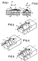
- Figures 1 and 2 are deliberately aligned at the level of the optical axis common to the laser and to the fiber.
- Figure 1 shows a section in elevation at the plane of symmetry AA of the device
- Figure 2 shows a section in elevation at level BB of the end of the fiber facing the laser.
- This part of an optical head which is in fact more complex and comprises a housing and other electronic components, comprises at least one metal base 1, of shape and dimensions adapted as appropriate, but having the permanent character of serving base and reference plane R to the laser 2 and to the optical fiber 3.
- the latter is itself passed and fixed in a metallic cylindrical tip 4, according to a well-known technique which makes it possible to grasp the fiber in order to micromanipulate it , without breaking it.
- the means for fixing the fiber 3 in one position aligned with the laser transmitter tape 2 consist of at least two metal plates 5 and 6. Each has a side, preferably cut into an edge, which rests in a groove 7 and 8, respectively, hollowed in the base 1, parallel to the optical axis.
- the grooves 7 and 8 are sufficiently distant from each other so that the plates 5 and 6 can, under the effect of the forces of gravity, bear against the metal end piece 4. Since the grooves 7 and 8 are parallel to the optical axis, it follows that the plates 5 and 6 are in contact with a generator of the cylindrical tip 4: it is therefore a linear contact, easier to make than a contact between plans as is practiced in known art.
- the parts making up the system are only installed: they are not fixed. They will be fixed after the alignment between the optical axis of the laser 2 and the optical axis of the fiber 3 has been adjusted.
- FIG. 2 shows that each of the plates 5 and 6 can pivot around the groove 7 and 8, therefore having its own angle, in a system of polar coordinates.
- the combination of the angles of the two plates 5 and 6 makes it possible to center the fiber 3 along the axis Oy.
- the micromanipulator - which is not shown - can raise or lower the end piece 4 so as to align the fiber 3 on the laser 2 along the axis Ox.
- the end piece 4 varies in position, it moves plates 5 and 6: it is therefore finally in a polar coordinate system that the position of the optical fiber is adjusted, defined by the angle ⁇ made by one of plates 5 or 6 with the upper plane of the base 1, and the distance "d" at which the end piece 4 is tangent to said plate 5 or 6.
- the position of the fiber can also be defined by the two angles of the two plates 5 and 6.
- the adjustment of the distance between the laser 2 and the end of the fiber 3, along the axis Oz, can be carried out either before or after alignment along the axes x0y.
- the last step of the process consists in making the base, the plates and the end piece together by means of a few welding points, by power laser.
- FIG. 3 clearly shows the solder points 9 which fix the plates 5 and 6 on two generatrices of the cylindrical end piece 4, and the solder points 10 which fix the same plates on the base 1.
- the simplest case is obviously that in which only two plates 5 and 6 hold and orient the fiber 3 in its end piece 4. External stresses of different species can oblige to better immobilize the fiber 3, by means of 3 or 4 plates 11 , 12, as shown in FIGS. 4 and 5.
- the two plates 5 and 6 closest to the laser 2 are aligned and fixed first, and if an external stress tends to deform the system and to misalign the fiber 3, this constraint can be canceled by the action of plates 11 and / or 12, the most distant from laser 2.
- the metal parts of the system are made of a material that does not deform very much in temperature, for example a Fe-Ni-Co alloy such as Invar TM, Kovar TM or Dilver TM.
- a Fe-Ni-Co alloy such as Invar TM, Kovar TM or Dilver TM.
Landscapes
- Physics & Mathematics (AREA)
- General Physics & Mathematics (AREA)
- Optics & Photonics (AREA)
- Optical Couplings Of Light Guides (AREA)
- Light Receiving Elements (AREA)
- Led Device Packages (AREA)
- Semiconductor Lasers (AREA)
Claims (5)
- Verfahren zur Ausrichtung der optischen Achsen einer Lichtleitfaser und eines opto-elektronischen Halbleiterbauteils (2), das auf einer Basis (1) befestigt ist, deren Oberseite als Bezugsebene (R) dient, wobei gemäß diesem Verfahren die Lichtleitfaser (3), die mit einem metallischen Endstück (4) versehen ist, vor dem opto-elektronischen Bauteil (2) mit Hilfe mindestens zweier metallischer Plättchen (5, 6) in Flucht gebracht wird, die zu beiden Seiten der Faser (3) liegen, dadurch gekennzeichnet, daß die Plättchen (5, 6) sich einerseits in Rinnen (7, 8), die in die Bezugsebene (R) der Basis (1) der Vorrichtung eingeschnitten sind, und andererseits gegen das Endstück (4) der Faser (3) abstützen und daß die Winkel (α) der Plättchen (5, 6) mit dieser Ebene (R) so eingestellt werden, daß dadurch die Position der Faser (3) bestimmt wird.
- Verfahren nach Anspruch 1, dadurch gekennzeichnet, daß nach dem Erreichen der optischen Ausrichtung die metallischen Plättchen (5, 6) auf das metallische Endstück (4) und auf die Basis (1) durch Laserschweißpunkte (9, 10) aufgeschweißt werden.
- Verfahren nach Anspruch 1, dadurch gekennzeichnet, daß die Rinnen (7, 8) in die Basis (1) parallel zur optischen Achse eingeschnitten werden.
- Opto-elektronische Vorrichtung mit einer Lichtleitfaser (3), die mit einem metallischen Endstück (4) versehen ist und auf die optische Achse eines opto-elektronischen Halbleiterbauteils (2) ausgerichtet ist, das auf einer Basis (1) fixiert ist, deren Oberseite als Bezugsebene (R) dient, wobei die Faser mit Hilfe mindestens zweier metallischer Plättchen (5, 6), die sich zu beiden Seiten der Faser (3) befinden, fixiert ist, dadurch gekennzeichnet, daß sich die Plättchen (5, 6) je einerseits auf einer Mantellinie des metallischen Endstücks (4) und andererseits mit einer kantig geschnittenen Seite in einer Rinne (7, 8) abstützen, die in die Bezugsebene (R) der Basis (1) eingeschnitten ist, wobei jedes Plättchen (5, 6) einen Winkel (α) mit der Bezugsebene einschließt.
- Vorrichtung nach Anspruch 4, dadurch gekennzeichnet, daß die Rinnen (7, 8) parallel zur optischen Achse der Vorrichtung verlaufen und daß die Plättchen (5, 6) zu beiden Seiten des Endstücks (4) angeordnet sind.
Applications Claiming Priority (2)
| Application Number | Priority Date | Filing Date | Title |
|---|---|---|---|
| FR9012957A FR2668267B1 (fr) | 1990-10-19 | 1990-10-19 | Procede d'alignement des axes optiques d'une fibre et d'un composant optoelectronique, et dispositif obtenu par ce procede. |
| FR9012957 | 1990-10-19 |
Publications (2)
| Publication Number | Publication Date |
|---|---|
| EP0481876A1 EP0481876A1 (de) | 1992-04-22 |
| EP0481876B1 true EP0481876B1 (de) | 1995-04-19 |
Family
ID=9401394
Family Applications (1)
| Application Number | Title | Priority Date | Filing Date |
|---|---|---|---|
| EP91402749A Expired - Lifetime EP0481876B1 (de) | 1990-10-19 | 1991-10-15 | Justierverfahren der optischen Achsen von einer Faser und von einem optoelektronischen Bauelement und die mit diesem Verfahren hergestellte Vorrichtung |
Country Status (5)
| Country | Link |
|---|---|
| US (1) | US5210811A (de) |
| EP (1) | EP0481876B1 (de) |
| JP (1) | JPH0688923A (de) |
| DE (1) | DE69109047T2 (de) |
| FR (1) | FR2668267B1 (de) |
Families Citing this family (21)
| Publication number | Priority date | Publication date | Assignee | Title |
|---|---|---|---|---|
| GB9100680D0 (en) * | 1991-01-11 | 1991-02-27 | Gen Electric Co Plc | Optical fibre interface |
| FR2690996A1 (fr) * | 1992-05-07 | 1993-11-12 | Thomson Hybrides | Dispositif d'alignement optique entre un composant optoélectronique et un composant optique, et procédé d'alignement. |
| GB2296101B (en) * | 1994-12-12 | 1998-04-01 | Northern Telecom Ltd | Optically coupling optical fibres to injection lasers |
| US5857049A (en) * | 1997-05-05 | 1999-01-05 | Lucent Technologies, Inc., | Precision alignment of optoelectronic devices |
| US6227724B1 (en) * | 1999-01-11 | 2001-05-08 | Lightlogic, Inc. | Method for constructing an optoelectronic assembly |
| US6511236B1 (en) * | 1999-09-07 | 2003-01-28 | Intel Corporation | Optoelectronic assembly and method for fabricating the same |
| DE19904265C2 (de) * | 1999-02-03 | 2001-02-22 | Kufner Textilwerke Gmbh | Elastische Einlage, Verfahren zu deren Herstellung und Verwendung |
| GB0018534D0 (en) * | 2000-07-29 | 2000-09-13 | Agilent Technologies Inc | Optical Assembly and Method for Alignment therof |
| US6546172B2 (en) * | 2001-02-20 | 2003-04-08 | Avanti Optics Corporation | Optical device |
| US6443631B1 (en) | 2001-02-20 | 2002-09-03 | Avanti Optics Corporation | Optical module with solder bond |
| US6956999B2 (en) | 2001-02-20 | 2005-10-18 | Cyberoptics Corporation | Optical device |
| US6546173B2 (en) | 2001-02-20 | 2003-04-08 | Avanti Optics Corporation | Optical module |
| US20040212802A1 (en) * | 2001-02-20 | 2004-10-28 | Case Steven K. | Optical device with alignment compensation |
| FR2831279B1 (fr) * | 2001-10-18 | 2003-12-12 | Commissariat Energie Atomique | Procede et dispositif de connexion/deconnexion de fibre optique avec un composant optoelectronique |
| US20030155486A1 (en) * | 2002-02-15 | 2003-08-21 | Quantum Photonics | Method and apparatus for co-axial alignment through non-coaxial means |
| US7430081B2 (en) * | 2002-02-28 | 2008-09-30 | Emcore Corporation | Sub-micron adjustable mount for supporting a component and method |
| US7126078B2 (en) | 2002-02-28 | 2006-10-24 | Emcore Corporation | Sub-micron adjustable mount for supporting a component and method |
| US6669379B2 (en) * | 2002-04-01 | 2003-12-30 | Princeton Lightwave, Inc. | Method of attaching optical fiber in alignment with a light source in an optical module |
| CN1675572A (zh) * | 2002-08-20 | 2005-09-28 | 赛博光学公司 | 能够调整高度的光学对准安装座 |
| JP5639220B2 (ja) * | 2012-12-21 | 2014-12-10 | 古河電気工業株式会社 | 光ファイバの固定構造、半導体レーザモジュール、光ファイバの固定方法 |
| CN110632715A (zh) * | 2019-09-24 | 2019-12-31 | 武汉光迅科技股份有限公司 | 一种光模块 |
Family Cites Families (8)
| Publication number | Priority date | Publication date | Assignee | Title |
|---|---|---|---|---|
| EP0104882B1 (de) * | 1982-09-29 | 1986-08-27 | THE GENERAL ELECTRIC COMPANY, p.l.c. | Montageanordnungen zum Verbinden einer optischen Faser |
| DE3431775A1 (de) * | 1984-08-29 | 1986-03-13 | Siemens AG, 1000 Berlin und 8000 München | Anordnung zur justierbaren ausrichtung eines lichtwellenleiters und verfahren zur justierung mit hilfe einer solchen anordnung |
| JPS61201208A (ja) * | 1985-03-04 | 1986-09-05 | Nec Corp | 光フアイバ−結合構造 |
| GB8508280D0 (en) * | 1985-03-29 | 1985-05-09 | British Telecomm | Optical component mounting |
| DE3531734A1 (de) * | 1985-09-05 | 1987-03-12 | Siemens Ag | Einrichtung zur positionierung eines halbleiterlasers mit selbstjustierender wirkung fuer eine anzukoppelnde glasfaser |
| DE3630795C2 (de) * | 1986-09-10 | 1994-11-24 | Ant Nachrichtentech | Verfahren zum Ankoppeln eines Lichtwellenleiters an ein optoelektronisches Sende- oder Empfangselement |
| JPH01225909A (ja) * | 1988-03-07 | 1989-09-08 | Oki Electric Ind Co Ltd | 光結合器 |
| JPH01296204A (ja) * | 1988-05-25 | 1989-11-29 | Oki Electric Ind Co Ltd | 光半導体結合器の製造方法 |
-
1990
- 1990-10-19 FR FR9012957A patent/FR2668267B1/fr not_active Expired - Lifetime
-
1991
- 1991-10-15 DE DE69109047T patent/DE69109047T2/de not_active Expired - Fee Related
- 1991-10-15 EP EP91402749A patent/EP0481876B1/de not_active Expired - Lifetime
- 1991-10-18 US US07/779,260 patent/US5210811A/en not_active Expired - Fee Related
- 1991-10-18 JP JP3297637A patent/JPH0688923A/ja not_active Withdrawn
Also Published As
| Publication number | Publication date |
|---|---|
| FR2668267B1 (fr) | 1992-12-11 |
| US5210811A (en) | 1993-05-11 |
| EP0481876A1 (de) | 1992-04-22 |
| DE69109047D1 (de) | 1995-05-24 |
| JPH0688923A (ja) | 1994-03-29 |
| DE69109047T2 (de) | 1995-08-31 |
| FR2668267A1 (fr) | 1992-04-24 |
Similar Documents
| Publication | Publication Date | Title |
|---|---|---|
| EP0481876B1 (de) | Justierverfahren der optischen Achsen von einer Faser und von einem optoelektronischen Bauelement und die mit diesem Verfahren hergestellte Vorrichtung | |
| EP0205359B1 (de) | Optoelektronischer Zweirichtungsbauteil, der einen optischen Koppler bildet | |
| EP0304182B1 (de) | Mit einem Fiberende versehener optoelektronischer Wandler | |
| EP0138630B1 (de) | Vorrichtung zur Verbindung einer optischen Faser mit einem Photodetektor und Verfahren zu ihrer Positionierung | |
| EP0146867B1 (de) | Optischer Dämpfungsregler für Kupplung von optischen Fasern | |
| EP0183124A1 (de) | Optische Lichtquelle | |
| FR2545617A1 (fr) | Structure de support pour la fixation de fibres optiques et de lentilles et procede pour leur preparation ainsi que dispositif les utilisant | |
| FR2815140A1 (fr) | Procede et dispositif d'alignement passif de guides de lumiere et de composants optoelectriques et systeme optique utilisant ce dispositif | |
| FR2668268A1 (fr) | Dispositif d'alignement d'une fibre optique et d'un composant optoelectronique. | |
| EP0026124A1 (de) | Optoelektrische Spitze mit einem faseroptischen Ende sehr kleinen Durchmessers und Verbindungsvorrichtung mit einer solchen Spitze | |
| EP0581671A1 (de) | Verfahren zur Ankopplung einer Glasfaser an einen optischen Baustein auf einem gemeinsamen Substrat | |
| FR2690996A1 (fr) | Dispositif d'alignement optique entre un composant optoélectronique et un composant optique, et procédé d'alignement. | |
| EP0326993A1 (de) | Ausrichteverfahren, insbesondere für optische Bauteile | |
| EP0121460B1 (de) | Aufnahmestück für optische Fasern für eine Kupplungsvorrichtung und Verfahren zur Herstellung einer solchen Vorrichtung | |
| CA2072411C (fr) | Dispositif a fibre optique transversalement anisotrope et son procede de fabrication | |
| EP0090724B1 (de) | Vorrichtung zum Verbinden von optischen Fasern und Verfahren zu deren Benutzung | |
| FR2661005A1 (fr) | Dispositif d'alignement et de fixation d'une fibre optique devant un laser semiconducteur. | |
| EP0224806A1 (de) | Spannvorrichtung für optische Fasern | |
| EP2937723B1 (de) | Verfahren zur befestigung einer optischen faser mit einer halterung einer laserdiode | |
| EP0376840B1 (de) | Vorrichtung zur Befestigung eines zerbrechlichen Gegenstandes, z.B. ein Spiegel | |
| EP1160602A1 (de) | Ausrichtung eines Flipchiplasers in einer schrägen Position auf einer Montageebene mit Ausrichtpfosten | |
| EP0444566B1 (de) | Schneidezange mit kleiner Sperre zum Schneiden von optischen Fasern | |
| EP0768548A1 (de) | Gerät zum Erleichtern der Herstellung optischer Faserverbindungen | |
| FR2737310A1 (fr) | Procede et dispositif de couplage entre une fibre optique et un laser ou un photodetecteur | |
| FR2698453A1 (fr) | Procédé de couplage d'une fibre optique avec un composant optoélectronique et dispositif de couplage. |
Legal Events
| Date | Code | Title | Description |
|---|---|---|---|
| PUAI | Public reference made under article 153(3) epc to a published international application that has entered the european phase |
Free format text: ORIGINAL CODE: 0009012 |
|
| AK | Designated contracting states |
Kind code of ref document: A1 Designated state(s): DE GB IT NL SE |
|
| 17P | Request for examination filed |
Effective date: 19920518 |
|
| 17Q | First examination report despatched |
Effective date: 19940301 |
|
| RAP1 | Party data changed (applicant data changed or rights of an application transferred) |
Owner name: THOMSON-CSF SEMICONDUCTEURS SPECIFIQUES |
|
| GRAA | (expected) grant |
Free format text: ORIGINAL CODE: 0009210 |
|
| AK | Designated contracting states |
Kind code of ref document: B1 Designated state(s): DE GB IT NL SE |
|
| ITF | It: translation for a ep patent filed | ||
| REF | Corresponds to: |
Ref document number: 69109047 Country of ref document: DE Date of ref document: 19950524 |
|
| GBT | Gb: translation of ep patent filed (gb section 77(6)(a)/1977) |
Effective date: 19950427 |
|
| PLBE | No opposition filed within time limit |
Free format text: ORIGINAL CODE: 0009261 |
|
| STAA | Information on the status of an ep patent application or granted ep patent |
Free format text: STATUS: NO OPPOSITION FILED WITHIN TIME LIMIT |
|
| RAP2 | Party data changed (patent owner data changed or rights of a patent transferred) |
Owner name: THOMSON-CSF SEMICONDUCTEURS SPECIFIQUES |
|
| 26N | No opposition filed | ||
| NLT2 | Nl: modifications (of names), taken from the european patent patent bulletin |
Owner name: THOMSON-CSF SEMICONDUCTEURS SPECIFIQUES |
|
| PGFP | Annual fee paid to national office [announced via postgrant information from national office to epo] |
Ref country code: GB Payment date: 19960918 Year of fee payment: 6 |
|
| PGFP | Annual fee paid to national office [announced via postgrant information from national office to epo] |
Ref country code: SE Payment date: 19960919 Year of fee payment: 6 Ref country code: DE Payment date: 19960919 Year of fee payment: 6 |
|
| PGFP | Annual fee paid to national office [announced via postgrant information from national office to epo] |
Ref country code: NL Payment date: 19960926 Year of fee payment: 6 |
|
| PG25 | Lapsed in a contracting state [announced via postgrant information from national office to epo] |
Ref country code: GB Free format text: LAPSE BECAUSE OF NON-PAYMENT OF DUE FEES Effective date: 19971015 |
|
| PG25 | Lapsed in a contracting state [announced via postgrant information from national office to epo] |
Ref country code: SE Free format text: LAPSE BECAUSE OF NON-PAYMENT OF DUE FEES Effective date: 19971016 |
|
| PG25 | Lapsed in a contracting state [announced via postgrant information from national office to epo] |
Ref country code: NL Free format text: LAPSE BECAUSE OF NON-PAYMENT OF DUE FEES Effective date: 19980501 |
|
| GBPC | Gb: european patent ceased through non-payment of renewal fee |
Effective date: 19971015 |
|
| NLV4 | Nl: lapsed or anulled due to non-payment of the annual fee |
Effective date: 19980501 |
|
| PG25 | Lapsed in a contracting state [announced via postgrant information from national office to epo] |
Ref country code: DE Free format text: LAPSE BECAUSE OF NON-PAYMENT OF DUE FEES Effective date: 19980701 |
|
| EUG | Se: european patent has lapsed |
Ref document number: 91402749.5 |
|
| PG25 | Lapsed in a contracting state [announced via postgrant information from national office to epo] |
Ref country code: IT Free format text: LAPSE BECAUSE OF NON-PAYMENT OF DUE FEES;WARNING: LAPSES OF ITALIAN PATENTS WITH EFFECTIVE DATE BEFORE 2007 MAY HAVE OCCURRED AT ANY TIME BEFORE 2007. THE CORRECT EFFECTIVE DATE MAY BE DIFFERENT FROM THE ONE RECORDED. Effective date: 20051015 |