EP0482336A1 - Schnittstellenverfahren für einen schaltbaren Sender-Empfänger - Google Patents
Schnittstellenverfahren für einen schaltbaren Sender-Empfänger Download PDFInfo
- Publication number
- EP0482336A1 EP0482336A1 EP91115419A EP91115419A EP0482336A1 EP 0482336 A1 EP0482336 A1 EP 0482336A1 EP 91115419 A EP91115419 A EP 91115419A EP 91115419 A EP91115419 A EP 91115419A EP 0482336 A1 EP0482336 A1 EP 0482336A1
- Authority
- EP
- European Patent Office
- Prior art keywords
- driver
- differential
- interface device
- receiver
- ended
- Prior art date
- Legal status (The legal status is an assumption and is not a legal conclusion. Google has not performed a legal analysis and makes no representation as to the accuracy of the status listed.)
- Withdrawn
Links
Images





Classifications
-
- H—ELECTRICITY
- H03—ELECTRONIC CIRCUITRY
- H03K—PULSE TECHNIQUE
- H03K19/00—Logic circuits, i.e. having at least two inputs acting on one output; Inverting circuits
- H03K19/0175—Coupling arrangements; Interface arrangements
- H03K19/0185—Coupling arrangements; Interface arrangements using field effect transistors only
- H03K19/018592—Coupling arrangements; Interface arrangements using field effect transistors only with a bidirectional operation
-
- G—PHYSICS
- G06—COMPUTING OR CALCULATING; COUNTING
- G06F—ELECTRIC DIGITAL DATA PROCESSING
- G06F13/00—Interconnection of, or transfer of information or other signals between, memories, input/output devices or central processing units
- G06F13/38—Information transfer, e.g. on bus
- G06F13/40—Bus structure
- G06F13/4063—Device-to-bus coupling
- G06F13/4068—Electrical coupling
- G06F13/4072—Drivers or receivers
-
- H—ELECTRICITY
- H03—ELECTRONIC CIRCUITRY
- H03K—PULSE TECHNIQUE
- H03K19/00—Logic circuits, i.e. having at least two inputs acting on one output; Inverting circuits
- H03K19/0175—Coupling arrangements; Interface arrangements
- H03K19/0185—Coupling arrangements; Interface arrangements using field effect transistors only
- H03K19/018585—Coupling arrangements; Interface arrangements using field effect transistors only programmable
Definitions
- the present invention relates to data communications systems and, in particular, to a line interface device that is switchable between single-ended and differential operating modes.
- An interface circuit amplifies the low voltage/low current levels at the computer output ports either for transmission over a transmission medium (e.g., twisted pair, coaxial cable) or for use by higher voltage/higher current peripheral devices (e.g., displays, printers).
- a transmission medium e.g., twisted pair, coaxial cable
- higher voltage/higher current peripheral devices e.g., displays, printers
- a line interface circuit is a type of interface circuit that transfers digital information from a computer or peripheral device over a transmission line.
- a bi-directional line interface circuit commonly referred to as a transceiver (TRANSmitter/reCEIVER), typically includes a line driver stage and receiver stage.
- the line driver amplifies digital signal outputs from the computer system so that they can be properly transmitted on the transmission medium.
- Conventional line drivers usually include level shifting capability to provide compatibility with different integrated circuit technologies (e.g. TTL) that might be used in the computer's internal logic.
- the receiver is typically a differential amplifier that receives signals from a two-wire transmission channel and provides a single-ended output representative of the digital information received on that channel.
- receiver 14 is disabled by placing its output in the high impedance state; a system output is thus applied to driver 12 via the I/O line which, in turn, provides its differential outputs DO+/RI+ and DO-/RI- to the transmission medium.
- the transceiver's line driver and receiver are single input-single output circuits.
- Line interface circuits may be designed for general-purpose applications or may be designed for a specific, industry standard data-communications configuration.
- SCSI Small Computer System Interface
- ANS American National Standard X3.131 defines one line interface configuration for single-ended operation and a second line interface configuration for differential operation.
- a transceiver interface device in accordance with the present invention includes line driver and receiver features which allow it to operate in either differential or single-ended computer systems.
- the line driver output levels are switchable between TTL levels and non-TTL levels having small differential swings.
- the receiver is switchable between a differential threshold and a single-ended TTL threshold.
- the line driver outputs when in the differential mode, may both be in the high impedance state at the same time; in the single-ended mode, the line driver outputs may both be in the high impedance state at the same time or have one output in the high impedance state while the other output is active.
- the state of the DIFFSENS pin or the driver enable signal on the SCSI interface is used for mode switching between differential and single-ended operation.
- Fig. 1 is a block diagram illustrating a conventional differential transceiver.
- Fig. 2 is a block diagram illustrating a switchable transceiver interface device in accordance with the present invention.
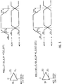
- Fig. 3 illustrates driver stage output levels switchable between TTL levels and non-TTL levels in a switchable transceiver interface-device in accordance with the present invention.
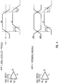
- Fig. 4 illustrates receiver stage threshold levels switchable between single-ended TTL levels and differential receiver threshold levels in a switchable transceiver interface device in accordance with the present invention.
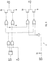
- Fig. 5 illustrates the ability to place only one output of a differential driver in a switchable transceiver interface device in accordance with the present invention in a high impedance state.
- Fig. 6 is a circuit diagram illustrating use of the SCSI DIFFSENS pin or driver enable signal for deriving the transceiver mode signal for switching between different operating modes of a switchable transceiver interface device in accordance with the present invention.
- Fig. 7 is a circuit diagram illustrating a driver output stage that switches between a TTL and non-TTL output voltage.
- Fig. 8 is a circuit diagram illustrating a differential receiver input stage that switches from a differential input stage to a single-ended input stage with TTL threshold.
- Fig. 9 is a circuit diagram illustrating a differential driver output stage wherein either one or both outputs can be placed in the high impedance state.
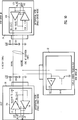
- Fig. 10 illustrates switchable transceivers operating in the single-ended mode in accordance with the present invention.
- Fig. 11 illustrates switchable transceivers operating in the differential mode in accordance with the present invention.
- Fig. 2 shows a block diagram of a switchable transceiver interface device 20 that includes a differential driver 22 and a differential receiver 24. Both the differential outputs DO+/RI+ and DO-/RI- of driver 22 and the inputs of the receiver 24 are connected to the lines of a differential transmission channel.
- the transceiver 20 may be configured in either a differential mode or a single-ended mode to enable it to be used in either differential or single-ended Small Computer System Interface (SCSI) systems.
- SCSI Small Computer System Interface
- the logic state of a mode control input signal to driver 22 determines whether the driver output levels are TTL levels or are non-TTL levels.
- the logic state of the mode control input signal to receiver 24 determines whether the receiver threshold is differential or single-ended TTL.
- a driver enable signal is used to place both outputs of driver 22 in the high impedance state when the transceiver 20 is in the differential mode, but may also be used to place the active driver output in the high impedance state when the transceiver 20 is in the single-ended mode (In the single-ended mode, one driver output is automatically placed in the high impedance state for as long as the transceiver is in the single-ended mode).
- the mode input used to switch the operating modes of the transceiver 20 is derived from the SCSI standard DIFFSENS pin or driver enable line.
- TTL VOH level is approximately 2.8V minimum; the TTL VOL level is approximately 0.4V maximum.
- Fig. 3 further shows that when the mode control input to the driver 22 is in a second logic state (Mode 2), then the driver 22 generates non-TTL output levels at its outputs.
- Mode 2 VOH output level remains at the 2.8V TTL level, while the VOL output level is adjusted to approximately 2.0V.
- the mode control input to receiver 24 is the first logic state (Mode 1)
- the non-inverting input is the input to the single-ended receiver in Mode 2.
- driver enable signal DE is utilizable for placing the outputs of driver 22 in the high impedance state in a variety of configurations.
- the transceiver 20 switches between single-ended operation and differential operation depending upon the state of the mode control signal.
- the mode control signal is derived from the DIFFSENS pin or driver enable signal defined in the SCSI standard.
- Fig. 6 shows an SCSI differential sense/driver enable circuit 26 used to produce the mode control signal, identifed as MODE ⁇ in Fig. 6.
- the driver enable signal is used as a safety feature to disable the outputs of differential drivers when a differential-type SCSI transceiver driver is connected to a single-ended SCSI system.
- the DIFFSENS line is connected to ground, causing the DIFFSENS node to go low.
- Gate 28 then provides a low driver enable signal.
- the output of gate 28 or the DIFFSENS pin is used as the mode control signal MODE ⁇ for the transceiver 20.
- Fig. 7 shows a driver 22 that switches between a TTL and non-TTL output voltage, as described above in conjunction with Fig. 3.
- the output low voltage VOL is switched.
- the mode control signal MODE ⁇ goes low, active pull-down gate B is selected.
- Gate B has a low resistance channel that pulls the output VOL down to a TTL low (0.4V), which is compatible with single-ended SCSI systems.
- the mode control signal MODE ⁇ goes high, gate A is selected and the output low voltage VOL is higher (about 2V) since gate A has a higher resistance channel than does gate B.
- Fig. 8 shows a differential receiver input stage 24 that switches from a differential input stage to a single-ended input stage with a TTL threshold (about 1.3V), as described above in conjunction with Fig. 4.
- mode control signal MODE ⁇ When configured as a single-ended input stage, i.e., mode control signal MODE ⁇ is low, single-ended signals are input via the non-inverting input.
- mode control signal MODE ⁇ When configured as a differential input stage, i.e., mode control signal MODE ⁇ is high, differential signals are input across the inverting and non-inverting inputs.
- Fig. 9 shows a differential driver ouptut stage 22 wherein either one or both outputs DO+, DO- can be placed in the high impedance state.
- the inverting output DO- is placed in the high impedance state when the mode control signal MODE ⁇ goes low (the inverting output is grounded when connected to a single-ended SCSI system, so it must be placed in the high impedance state).
- the mode control signal MODE ⁇ low single-ended mode
- the state of the non-inverting output is controlled by the driver enable signal DE (active for DE high, high impedance state for DE low.
- the mode control signal MODE ⁇ high both outputs DO+, DO- are controlled by the driver enable signal DE (active for DE high, high impedance state for DE low).
- Fig. 10 shows an example of switchable differential transceivers in accordance with the present invention operating in the single-ended mode.
- a host computer system 30 communicates with a #1 disk drive 32 and a #2 disk drive 34 via an 18-bit parallel bus. Only one of the eighteen two-wire transmission paths is illustrated in Fig. 10.
- one of the two lines is biased to +3V from a +5V supply.
- the second line of the pair is tied to ground.
- the state of the non-inverting driver output (active or high impedance) depends on the logic state of the driver enable signal DE.
- Fig. 11 shows an example of switchable differential transceivers in accordance with the present invention operating in the differential mode.
- SCSI device #1 through SCSI device #8 are connected to an 18-bit parallel bus which serves as the transmission medium for a computer Input/Output system, e.g., a peripheral bus. Again, only one of the eighteen two-wire transmission paths is illustrated. Both of the lines are biased from a +5V supply.
- SCSI device #8 includes a switchable transceiver 20d which is configured as a differential receiver. That is, with the mode control set high and the enable control DE/ RE ⁇ set low, receiver 24 is set to a differential threshold and the differential outputs DO+ and DO- of driver 22 are both placed in the high impedance state.
Landscapes
- Engineering & Computer Science (AREA)
- Computer Hardware Design (AREA)
- General Engineering & Computer Science (AREA)
- Physics & Mathematics (AREA)
- Computing Systems (AREA)
- Theoretical Computer Science (AREA)
- Mathematical Physics (AREA)
- General Physics & Mathematics (AREA)
- Dc Digital Transmission (AREA)
- Logic Circuits (AREA)
- Bidirectional Digital Transmission (AREA)
- Memory System (AREA)
- Small-Scale Networks (AREA)
Applications Claiming Priority (2)
| Application Number | Priority Date | Filing Date | Title |
|---|---|---|---|
| US07/588,011 US5243623A (en) | 1990-09-25 | 1990-09-25 | Switchable multi-mode transceiver interface device |
| US588011 | 1990-09-25 |
Publications (1)
| Publication Number | Publication Date |
|---|---|
| EP0482336A1 true EP0482336A1 (de) | 1992-04-29 |
Family
ID=24352082
Family Applications (1)
| Application Number | Title | Priority Date | Filing Date |
|---|---|---|---|
| EP91115419A Withdrawn EP0482336A1 (de) | 1990-09-25 | 1991-09-12 | Schnittstellenverfahren für einen schaltbaren Sender-Empfänger |
Country Status (3)
| Country | Link |
|---|---|
| US (1) | US5243623A (de) |
| EP (1) | EP0482336A1 (de) |
| JP (1) | JP3115046B2 (de) |
Cited By (15)
| Publication number | Priority date | Publication date | Assignee | Title |
|---|---|---|---|---|
| EP0575124A3 (en) * | 1992-06-15 | 1996-07-24 | Fujitsu Ltd | Semiconductor integrated circuit with input/output interface adapted for small-amplitude operation |
| WO1996037958A1 (en) * | 1995-05-26 | 1996-11-28 | National Semiconductor Corporation | Supply and interface configurable input/output buffer |
| EP0599016B1 (de) * | 1992-11-25 | 1998-03-11 | Motorola, Inc. | Sender/Empfänger Schaltung |
| WO2000021193A1 (en) * | 1998-10-05 | 2000-04-13 | Koninklijke Philips Electronics N.V. | If amplifier |
| NL1007809C2 (nl) * | 1996-12-18 | 2002-03-12 | Sony Corp | Middenfrequentie versterkerschakeling. |
| WO2002029581A3 (en) * | 2000-10-05 | 2003-04-17 | Sun Microsystems Inc | Configurable differential/single ended i/o |
| WO2004102804A3 (en) * | 2003-05-09 | 2005-08-11 | Rambus Inc | Method and apparatus for signal reception using ground termination and/or non-ground termination |
| EP1476945A4 (de) * | 2002-02-19 | 2007-10-10 | Rambus Inc | Verfahren und vorrichtung zur wählbaren bereitstellung von asymmetrischer und symmetrischer zeichengabe mit steuerbarer impedanz und übergangszeit |
| US7408378B2 (en) | 2003-12-19 | 2008-08-05 | Rambus Inc. | Calibration methods and circuits for optimized on-die termination |
| WO2008065515A3 (en) * | 2006-11-28 | 2008-11-06 | Nokia Corp | Control method for fast and slow data transmission for serial interface |
| US7525338B2 (en) | 2003-09-08 | 2009-04-28 | Rambus Inc. | Calibration methods and circuits for optimized on-die termination |
| EP1446883A4 (de) * | 2001-11-02 | 2010-05-05 | Nokia Corp | Mehrmoden-e/a-schaltkreise, die störungsarme zeichengabeschemata für schnelle digitale schnittstellen unterstützen |
| CN101379705B (zh) * | 2006-02-08 | 2012-07-04 | 京瓷公司 | 用于连接双导线全双工总线和双向单导线总线的电平移动多路复用电路 |
| WO2015012958A1 (en) * | 2013-07-22 | 2015-01-29 | Raytheon Company | Differential-to-single-ended transmission line interface |
| WO2017172002A1 (en) * | 2016-03-31 | 2017-10-05 | Qualcomm Incorporated | Electrostatic discharge (esd) isolated input/output (i/o) circuits |
Families Citing this family (43)
| Publication number | Priority date | Publication date | Assignee | Title |
|---|---|---|---|---|
| DE69226150T2 (de) * | 1991-11-05 | 1999-02-18 | Hsu Fu Chieh | Redundanzarchitektur für Schaltungsmodul |
| US5831467A (en) * | 1991-11-05 | 1998-11-03 | Monolithic System Technology, Inc. | Termination circuit with power-down mode for use in circuit module architecture |
| US5498990A (en) * | 1991-11-05 | 1996-03-12 | Monolithic System Technology, Inc. | Reduced CMOS-swing clamping circuit for bus lines |
| WO1994003901A1 (en) | 1992-08-10 | 1994-02-17 | Monolithic System Technology, Inc. | Fault-tolerant, high-speed bus system and bus interface for wafer-scale integration |
| US5978877A (en) * | 1993-03-31 | 1999-11-02 | Fujitsu Limited | Translating SCSI bus control and/or data signals between differential and single-ended formats |
| US5715409A (en) * | 1993-05-24 | 1998-02-03 | I-Tech Corporation | Universal SCSI electrical interface system |
| US5517487A (en) * | 1993-07-19 | 1996-05-14 | Modicon, Inc. | System for increasing the capacity of existing local area networks that use shielded twisted wire pair medium |
| US5379405A (en) * | 1993-09-15 | 1995-01-03 | Unisys Corporation | SCSI converter with simple logic circuit arbitration for providing bilateral conversion between single ended signals and differential signals |
| US5737364A (en) * | 1994-02-18 | 1998-04-07 | Telebit Corporation | Serial communications interface that supports multiple interface standards |
| US5485488A (en) * | 1994-03-29 | 1996-01-16 | Apple Computer, Inc. | Circuit and method for twisted pair current source driver |
| US5469473A (en) * | 1994-04-15 | 1995-11-21 | Texas Instruments Incorporated | Transceiver circuit with transition detection |
| US5541535A (en) * | 1994-12-16 | 1996-07-30 | International Business Machines Corporation | CMOS simultaneous transmission bidirectional driver/receiver |
| US5539333A (en) * | 1995-01-23 | 1996-07-23 | International Business Machines Corporation | CMOS receiver circuit |
| US5525914A (en) * | 1995-01-23 | 1996-06-11 | International Business Machines Corporation | CMOS driver circuit |
| DE69523136T2 (de) * | 1995-01-30 | 2002-06-20 | Alcatel Sa | Übertragungsverfahren und Sender mit einem entkoppelten niedrigen Pegel und mit mindestens einem gekoppelten hohen Pegel, Schnittstellenschaltung und Systemkomponente für ein Telekommunikationsnetzwerk, die einen solchen Sender enthalten |
| DE19503460C1 (de) * | 1995-02-03 | 1996-03-07 | Daimler Benz Ag | Fehlertolerante Endstufe für ein digitales Zweileiterbus-Datenkommunikationssystem |
| JPH08274718A (ja) * | 1995-03-29 | 1996-10-18 | Nec Corp | インタフェース装置 |
| US5970255A (en) * | 1995-10-16 | 1999-10-19 | Altera Corporation | System for coupling programmable logic device to external circuitry which selects a logic standard and uses buffers to modify output and input signals accordingly |
| US5864715A (en) * | 1996-06-21 | 1999-01-26 | Emc Corporation | System for automatically terminating a daisy-chain peripheral bus with either single-ended or differential termination network depending on peripheral bus signals and peripheral device interfaces |
| US6070211A (en) * | 1997-06-11 | 2000-05-30 | International Business Machines Corporation | Driver/receiver circuitry for enhanced PCI bus with differential signaling |
| US5922062A (en) * | 1997-06-26 | 1999-07-13 | Vlsi Technology, Inc. | Combined IDE and SCSI disk controller interface for common hardware reference platforms |
| KR100520858B1 (ko) * | 1998-10-09 | 2005-12-21 | 유티스타콤코리아 유한회사 | 디퍼런셜 및 싱글-엔디드 방식을 겸용으로 실장 가능한 hdd구동 장치 및 방법 |
| US6703866B1 (en) * | 2000-12-19 | 2004-03-09 | International Business Machines Corporation | Selectable interface for interfacing integrated circuit modules |
| US7068073B2 (en) * | 2001-03-17 | 2006-06-27 | Hewlett-Packard Development Company, L.P. | Circuit for switching one or more HVD transceivers |
| US7401162B2 (en) * | 2003-07-22 | 2008-07-15 | Psion Teklogix Inc. | Multi-functional port |
| KR100715438B1 (ko) * | 2005-08-05 | 2007-05-09 | 삼성전자주식회사 | 디스플레이장치 |
| US7953162B2 (en) * | 2006-11-17 | 2011-05-31 | Intersil Americas Inc. | Use of differential pair as single-ended data paths to transport low speed data |
| US20080140907A1 (en) * | 2006-12-06 | 2008-06-12 | Dreps Daniel M | Multimodal Memory Controllers |
| US20080189457A1 (en) * | 2006-12-06 | 2008-08-07 | International Business Machines Corporation | Multimodal memory controllers |
| JP4960833B2 (ja) * | 2007-10-31 | 2012-06-27 | パナソニック株式会社 | シングルエンド伝送及び差動伝送の切替えが可能なインタフェース回路 |
| JP2010028751A (ja) * | 2008-07-24 | 2010-02-04 | Toshiba Corp | コンプリメンタリー光配線装置 |
| US7961007B2 (en) * | 2009-04-30 | 2011-06-14 | Apple Inc. | Receiver to match delay for single ended and differential signals |
| JP5296620B2 (ja) * | 2009-07-06 | 2013-09-25 | ルネサスエレクトロニクス株式会社 | 信号中継回路 |
| JP2011019189A (ja) * | 2009-07-10 | 2011-01-27 | Fujitsu Semiconductor Ltd | 半導体集積回路 |
| JP5136587B2 (ja) | 2010-04-01 | 2013-02-06 | 株式会社デンソー | 増幅回路、信号処理回路および半導体集積回路装置 |
| US8543753B2 (en) * | 2011-04-06 | 2013-09-24 | International Business Machines Corporation | Multi-use physical architecture |
| US8432185B2 (en) | 2011-05-25 | 2013-04-30 | Apple Inc. | Receiver circuits for differential and single-ended signals |
| US8410814B2 (en) | 2011-06-16 | 2013-04-02 | Apple Inc. | Receiver circuits for differential and single-ended signals |
| US9473205B2 (en) * | 2014-05-01 | 2016-10-18 | Microchip Technology Incorporated | Coaxial data communication with reduced EMI |
| US9866270B2 (en) | 2014-05-01 | 2018-01-09 | Microchip Technology Incorporated | Coaxial data communication with reduced EMI |
| US20230148367A1 (en) * | 2021-11-11 | 2023-05-11 | Texas Instruments Incorporated | System and method for multi-mode receiver |
| US12210404B2 (en) | 2022-12-01 | 2025-01-28 | Nxp Usa, Inc. | Lockup detection circuit for an eUSB repeater |
| US12229071B2 (en) * | 2022-12-01 | 2025-02-18 | Nxp Usa, Inc. | eUSB repeater for passing repeating mode packets between a differential bus and a single-ended bus |
Citations (1)
| Publication number | Priority date | Publication date | Assignee | Title |
|---|---|---|---|---|
| US3333113A (en) * | 1964-09-03 | 1967-07-25 | Bunker Ramo | Switching circuit producing output at one of two outputs or both outputs |
Family Cites Families (6)
| Publication number | Priority date | Publication date | Assignee | Title |
|---|---|---|---|---|
| US4254501A (en) * | 1979-03-26 | 1981-03-03 | Sperry Corporation | High impedance, Manchester (3 state) to TTL (2 wire, 2 state) transceiver for tapped bus transmission systems |
| IT1118946B (it) * | 1979-10-04 | 1986-03-03 | Cselt Centro Studi Lab Telecom | Ricetrasmettitore per trasmissione bidirezionale simultanea di segnali numerici su una linea unica |
| US4385394A (en) * | 1981-01-23 | 1983-05-24 | Datavision, Inc. | Universal interface for data communication systems |
| US4647912A (en) * | 1985-12-20 | 1987-03-03 | Tektronix, Inc. | Coupling discriminator and interface adaptor |
| US4825402A (en) * | 1986-04-04 | 1989-04-25 | Ncr Corporation | Multiconfigurable interface driver/receiver circuit for a computer printer peripheral adaptor |
| FR2623674B1 (fr) * | 1987-11-25 | 1990-04-20 | Peugeot | Dispositif de transmission d'informations pour vehicule automobile et procede de mise en oeuvre d'un tel dispositif |
-
1990
- 1990-09-25 US US07/588,011 patent/US5243623A/en not_active Expired - Lifetime
-
1991
- 1991-09-12 EP EP91115419A patent/EP0482336A1/de not_active Withdrawn
- 1991-09-25 JP JP03245395A patent/JP3115046B2/ja not_active Expired - Lifetime
Patent Citations (1)
| Publication number | Priority date | Publication date | Assignee | Title |
|---|---|---|---|---|
| US3333113A (en) * | 1964-09-03 | 1967-07-25 | Bunker Ramo | Switching circuit producing output at one of two outputs or both outputs |
Non-Patent Citations (1)
| Title |
|---|
| IBM TECHNICAL DISCLOSURE BULLETIN. vol. 30, no. 11, April 1988, NEW YORK, US pages 478 - 482; 'Electronically switchable interface circuit with multiple EIA protocol drivers and receivers.' * |
Cited By (39)
| Publication number | Priority date | Publication date | Assignee | Title |
|---|---|---|---|---|
| US6720804B2 (en) | 1992-05-15 | 2004-04-13 | Fujitsu Limited | Semiconductor integrated circuit with input/output interface adapted for small-amplitude operation |
| US6737893B2 (en) | 1992-06-15 | 2004-05-18 | Fujitsu Limited | Semiconductor integrated circuit with input/output interface adapted for small-amplitude operation |
| US5557221A (en) * | 1992-06-15 | 1996-09-17 | Fujitsu Limited | Semiconductor integrated circuit with input/output interface adapted for small-amplitude operation |
| US6034555A (en) * | 1992-06-15 | 2000-03-07 | Fujitsu Limited | Semiconductor integrated circuit with input/output interface adapted for small-amplitude operation |
| EP0575124A3 (en) * | 1992-06-15 | 1996-07-24 | Fujitsu Ltd | Semiconductor integrated circuit with input/output interface adapted for small-amplitude operation |
| US6492846B1 (en) | 1992-06-15 | 2002-12-10 | Fujitsu Limited | Semiconductor integrated circuit with input/output interface adapted for small-amplitude operation |
| US6744300B2 (en) | 1992-06-15 | 2004-06-01 | Fujitsu Limited | Semiconductor integrated circuit with input/output interface adapted for small-amplitude operation |
| US6707325B2 (en) | 1992-06-15 | 2004-03-16 | Fujitsu Limited | Semiconductor integrated circuit with input/output interface adapted for small-amplitude operation |
| EP0599016B1 (de) * | 1992-11-25 | 1998-03-11 | Motorola, Inc. | Sender/Empfänger Schaltung |
| WO1996037958A1 (en) * | 1995-05-26 | 1996-11-28 | National Semiconductor Corporation | Supply and interface configurable input/output buffer |
| US5612637A (en) * | 1995-05-26 | 1997-03-18 | National Semiconductor Corporation | Supply and interface configurable input/output buffer |
| NL1007809C2 (nl) * | 1996-12-18 | 2002-03-12 | Sony Corp | Middenfrequentie versterkerschakeling. |
| WO2000021193A1 (en) * | 1998-10-05 | 2000-04-13 | Koninklijke Philips Electronics N.V. | If amplifier |
| WO2002029581A3 (en) * | 2000-10-05 | 2003-04-17 | Sun Microsystems Inc | Configurable differential/single ended i/o |
| US8965304B2 (en) | 2001-11-02 | 2015-02-24 | Nokia Corporation | Multi-mode I/O circuitry supporting low interference signaling schemes for high speed digital interfaces |
| EP1446883A4 (de) * | 2001-11-02 | 2010-05-05 | Nokia Corp | Mehrmoden-e/a-schaltkreise, die störungsarme zeichengabeschemata für schnelle digitale schnittstellen unterstützen |
| EP1476945A4 (de) * | 2002-02-19 | 2007-10-10 | Rambus Inc | Verfahren und vorrichtung zur wählbaren bereitstellung von asymmetrischer und symmetrischer zeichengabe mit steuerbarer impedanz und übergangszeit |
| WO2004102804A3 (en) * | 2003-05-09 | 2005-08-11 | Rambus Inc | Method and apparatus for signal reception using ground termination and/or non-ground termination |
| US7102390B2 (en) | 2003-05-09 | 2006-09-05 | Rambus Inc. | Method and apparatus for signal reception using ground termination and/or non-ground termination |
| US9191243B2 (en) | 2003-09-08 | 2015-11-17 | Rambus Inc. | Calibration methods and circuits to calibrate drive current and termination impedance |
| US10270441B2 (en) | 2003-09-08 | 2019-04-23 | Rambus Inc. | Calibration methods and circuits to calibrate drive current and termination impedance |
| US7741868B2 (en) | 2003-09-08 | 2010-06-22 | Rambus Inc. | Calibration methods and circuits to calibrate drive current and termination impedance |
| US7928757B2 (en) | 2003-09-08 | 2011-04-19 | Rambus Inc. | Calibration methods and circuits to calibrate drive current and termination impedance |
| US11522544B2 (en) | 2003-09-08 | 2022-12-06 | Rambus Inc. | Calibration methods and circuits to calibrate drive current and termination impedance |
| US8278968B2 (en) | 2003-09-08 | 2012-10-02 | Rambus Inc. | Calibration methods and circuits to calibrate drive current and termination impedance |
| US10666254B2 (en) | 2003-09-08 | 2020-05-26 | Rambus Inc. | Calibration methods and circuits to calibrate drive current and termination impedance |
| US7525338B2 (en) | 2003-09-08 | 2009-04-28 | Rambus Inc. | Calibration methods and circuits for optimized on-die termination |
| US7564258B2 (en) | 2003-09-08 | 2009-07-21 | Rambus Inc. | Calibration methods and circuits to calibrate drive current and termination impedance |
| US9780784B2 (en) | 2003-09-08 | 2017-10-03 | Rambus Inc. | Calibration methods and circuits to calibrate drive current and termination impedance |
| US9391613B2 (en) | 2003-09-08 | 2016-07-12 | Rambus Inc. | Calibration methods and circuits to calibrate drive current and termination impedance |
| US7408378B2 (en) | 2003-12-19 | 2008-08-05 | Rambus Inc. | Calibration methods and circuits for optimized on-die termination |
| CN101379705B (zh) * | 2006-02-08 | 2012-07-04 | 京瓷公司 | 用于连接双导线全双工总线和双向单导线总线的电平移动多路复用电路 |
| WO2008065515A3 (en) * | 2006-11-28 | 2008-11-06 | Nokia Corp | Control method for fast and slow data transmission for serial interface |
| WO2015012958A1 (en) * | 2013-07-22 | 2015-01-29 | Raytheon Company | Differential-to-single-ended transmission line interface |
| US9270002B2 (en) | 2013-07-22 | 2016-02-23 | Raytheon Company | Differential-to-single-ended transmission line interface |
| WO2017172002A1 (en) * | 2016-03-31 | 2017-10-05 | Qualcomm Incorporated | Electrostatic discharge (esd) isolated input/output (i/o) circuits |
| CN108886363A (zh) * | 2016-03-31 | 2018-11-23 | 高通股份有限公司 | 静电放电(esd)隔离输入/输出(i/o)电路 |
| US10298010B2 (en) | 2016-03-31 | 2019-05-21 | Qualcomm Incorporated | Electrostatic discharge (ESD) isolated input/output (I/O) circuits |
| CN108886363B (zh) * | 2016-03-31 | 2022-01-14 | 高通股份有限公司 | 静电放电(esd)隔离输入/输出(i/o)电路 |
Also Published As
| Publication number | Publication date |
|---|---|
| US5243623A (en) | 1993-09-07 |
| JP3115046B2 (ja) | 2000-12-04 |
| JPH06224889A (ja) | 1994-08-12 |
Similar Documents
| Publication | Publication Date | Title |
|---|---|---|
| EP0482336A1 (de) | Schnittstellenverfahren für einen schaltbaren Sender-Empfänger | |
| EP0475711B1 (de) | System zur Datenübertragung zwischen Chips von integrierten Schaltungen | |
| US5864584A (en) | Circuitry for allowing two drivers to communicate with two receivers using one transmission line | |
| US6674313B2 (en) | Output buffer circuit | |
| US5694060A (en) | CMOS differential twisted-pair driver | |
| KR0167471B1 (ko) | Cmos 동시 전송 양방향 구동기/수신기 | |
| EP0289560B1 (de) | Abschluss für ein sende-empfangsgerät | |
| US20020172271A1 (en) | Transceiver | |
| WO1994022092A2 (en) | Method and apparatus for implementing a common mode level shift in a bus transceiver incorporating a high speed binary data transfer mode with a ternary control transfer mode | |
| US4994690A (en) | Split level bus | |
| WO1994022247A1 (en) | Bus transceiver with binary data transmission mode and ternary control transmission mode | |
| US8443125B2 (en) | Single pin read-write method and interface | |
| US4725836A (en) | Series port connection of a plurality of terminals to a master processor | |
| US5436887A (en) | Digital full-duplex transceiver | |
| US6788102B2 (en) | Transmitter with active differential termination | |
| EP0951680B1 (de) | Asymetrischer stromarttreiber für differentielle übertragungsleitungen | |
| EP0199338B1 (de) | Übertragungsschaltung | |
| US20040201401A1 (en) | Bi-directional impedance matching circuit | |
| US6774700B1 (en) | Current-mode logic differential signal generation circuit employing squelch | |
| JPS59501391A (ja) | デイジタル信号送信および受信装置 | |
| JPH10126316A (ja) | 終端装置 | |
| US20020070764A1 (en) | Output driver circuit with current detection | |
| US10187229B2 (en) | Bi-directional, full-duplex differential communication over a single conductor pair | |
| JPH03278744A (ja) | Rs232cラインレシーバic | |
| US5404057A (en) | Output circuit for outputting signals having different logical amplitudes |
Legal Events
| Date | Code | Title | Description |
|---|---|---|---|
| PUAI | Public reference made under article 153(3) epc to a published international application that has entered the european phase |
Free format text: ORIGINAL CODE: 0009012 |
|
| AK | Designated contracting states |
Kind code of ref document: A1 Designated state(s): DE FR GB IT |
|
| 17P | Request for examination filed |
Effective date: 19920529 |
|
| 17Q | First examination report despatched |
Effective date: 19950213 |
|
| STAA | Information on the status of an ep patent application or granted ep patent |
Free format text: STATUS: THE APPLICATION IS DEEMED TO BE WITHDRAWN |
|
| 18D | Application deemed to be withdrawn |
Effective date: 19950626 |