EP0482527A2 - System zur Schaltsteuerung zwischen Normal und Ersatz - Google Patents
System zur Schaltsteuerung zwischen Normal und Ersatz Download PDFInfo
- Publication number
- EP0482527A2 EP0482527A2 EP19910117830 EP91117830A EP0482527A2 EP 0482527 A2 EP0482527 A2 EP 0482527A2 EP 19910117830 EP19910117830 EP 19910117830 EP 91117830 A EP91117830 A EP 91117830A EP 0482527 A2 EP0482527 A2 EP 0482527A2
- Authority
- EP
- European Patent Office
- Prior art keywords
- spare
- current
- signal
- data processor
- switching
- Prior art date
- Legal status (The legal status is an assumption and is not a legal conclusion. Google has not performed a legal analysis and makes no representation as to the accuracy of the status listed.)
- Granted
Links
Images


Classifications
-
- G—PHYSICS
- G06—COMPUTING OR CALCULATING; COUNTING
- G06F—ELECTRIC DIGITAL DATA PROCESSING
- G06F11/00—Error detection; Error correction; Monitoring
- G06F11/07—Responding to the occurrence of a fault, e.g. fault tolerance
- G06F11/16—Error detection or correction of the data by redundancy in hardware
- G06F11/20—Error detection or correction of the data by redundancy in hardware using active fault-masking, e.g. by switching out faulty elements or by switching in spare elements
Definitions
- the present invention relates to a current-spare switching control system, more particularly, it relates to a current-spare switching control system provided for a data processing system having a current data processor, a spare data processor, a fault supervisor for supervising the fault of these processors, and switching units for switching from the current data processor to the spare data processor or vice versa.
- a data processing system has a current data processor and a spare data processor to ensure the reliability of data processing.
- the current data processor usually runs in a normal state, but it is immediately switched to the spare data processor when the fault occurs in the current data processor. In this case, the fault is detected by a fault supervisor which generates a switching signal to switch the switching units.
- the fault supervisor usually has an internal microprocessor for supervising the fault of these processors and generating the switching signal to switch the switching units.
- the switching units however, accidentally operate in error due to an error signal caused by reckless operation of the internal microprocessor of the fault supervisor. Accordingly, it is necessary to ensure correct operation of the switching units.
- the object of the present invention is to provide a current-spare switching control system enabling correct operation of switching units for switching from the current data processor to the spare data processor or vice versa.
- a current-spare switching control system provided for a data processing system having a current data processor, a spare data processor, a fault supervisor for supervising the fault of these processors, and switching units for switching from the current data processor to the spare data processor or vice versa.
- the above current-spare switching control system includes: a storage unit for temporarily storing data bits from the fault supervisor; a discrimination unit operatively connected to the storage unit for comparing the data bits with a reference signal and outputting a coincidence signal when the data bits coincide with the reference signal; an AND gate operatively connected to the discrimination unit and for inputting the coincidence signal and a write command from the fault supervisor, and outputting a write signal when the coincidence signal coincides with the write command; a register unit operatively connected to the AND gate for inputting a data bit from the fault supervisor and outputting a switching signal to switch from the current data processor to the spare data processor or vice versa.
- the storage unit has D-type flip-flop circuits each corresponding to each of data bits and inputting a write command from the fault supervisor; and the register unit has a D-type flip-flop circuit for inputting the data bit from the fault supervisor and the write signal from the AND gate, and outputting the switching signal.
- the current-spare switching control system further includes a leading edge detection circuit operatively connected to the D-type flip-flop circuit and the AND gate for inputting the write signal from the AND gate, detecting a leading edge of the write signal, and outputting a reset signal to the flip-flop circuits to clear the data bits therein.
- the current-spare switching control system includes: a shift register for sequentially inputting data bits from the fault supervisor and outputting data bits parallel therefrom in response to a shift command from the fault supervisor; a discrimination unit operatively connected to the shift register unit for comparing the data bits with a reference signal and outputting a coincidence signal when the data bits coincide with the reference signal; and a register operatively connected to the discrimination unit for outputting a switching signal to switch from the current data processor to the spare data processor or vice versa.
- the shift register has D-type flip-flop circuits, a first flip-flop circuit sequentially inputting data bits, and each flip-flop circuit outputting data bits in parallel in response to the shift command; and discrimination unit has a decoder for decoding data bits to produce the switching signal.
- the method includes the steps of: temporarily storing data bits from the fault supervisor; comparing the data bits with a reference signal and outputting a coincidence signal when the data bits coincide with the reference signal; generating a write signal when the coincidence signal coincides with a write command from the fault supervisor; and outputting a current-spare switching signal to switch from the current data processor to the spare data processor or vice versa, based on the data bit from the fault supervisor.
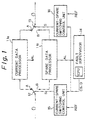
- FIG. 1 is a schematic block diagram of a data processing system applying the present invention.
- 11a denotes a current data processor and 11b denotes a spare processor.
- 12 and 13 denote switching units for switching from the current data processor 11a to the spare data processor 11b or vice versa.
- 14 denotes a fault supervisor.
- 15 and 16 denote current-spare switching control units each generating a switching signal S to switch the switching units 12 and 13.
- AL denotes an alarm signal generated from the current data processor 11a and the spare data processor 11b when the fault occurs in these processors
- REF denotes a reference signal generated from a host computer (not shown).
- the fault supervisor 14 has an internal microprocessor CPU and generates a command CS and data D from the internal microprocessor CPU to the current-spare switching control units 15 and 16 when the alarm signal AL is input from the current data processor 11a or the spare data processor 11b.
- Each of the current-spare switching control units 15 and 16 generates the switching signal S for simultaneously switching from the contact A to the contact B or vice versa in the switching units 12 and 13 when receiving the command CS, the data D and the reference signal REF, as explained in detail below.
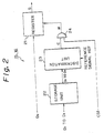
- FIG. 2 is a basic block diagram of the current-spare switching control unit according to an embodiment of the present invention.
- 21 denotes a register
- 22 denotes a storage unit
- 23 denotes a discrimination unit.
- a write command CS1, a bit D0, and bits D1 to D3 are input from the internal microprocessor CPU of the fault supervisor 14 of Fig. 1.
- the bit D0 is input to the register 21
- the bits D1 to D3 are input to the storage unit 22, and the write command CS1 is input to an AND gate 24.
- the storage unit 22 temporarily stores the bits D1 to D3.
- the discrimination unit 23 compares the bits D1 to D3 with the reference signal REF and outputs a coincidence signal C when the bits D1 to D3 coincide with the reference signal REF. Accordingly, when the write command CS1 is input to the AND gate 24, the AND gate 24 outputs a write signal W to the register 21 so that the bit D0 is written into the register 21. As a result, the register 21 outputs the switching signal S to the switching units 12 and 13.
- FIG. 3 is a basic block diagram of the current-spare switching control unit according to another embodiment of the present invention.
- 31 denotes a register
- 32 denotes a shift register
- 33 denotes a discrimination unit.
- the internal microprocessor CPU of the fault supervisor 14 generates a shift command SC and bits D1 to D3.
- the bits D1 to D3 are sequentially input to the shift register 32 in response to the shift command SC from the fault supervisor 14.
- the bits D1 to D3 are input in parallel to the discrimination unit 33 to compare the bits D1 to D3 with the reference signal REF.
- the discrimination unit 33 outputs the coincidence signal C when the bits D1 to D3 coincide with the reference signal REF.
- the register 31 outputs the switching signal S to the switching unit 12 and 13.
- Figure 4 is a detail circuit of the current-spare switching control unit shown in Fig. 2.
- 41 denotes a D-type flip-flop circuit corresponding to the register 21 of Fig. 2
- 42 denotes a memory circuit corresponding to the storage unit 22 of Fig. 2
- 43 denotes a discrimination circuit corresponding to the discrimination unit 23 of Fig. 2
- 44 denotes an AND gate corresponding to the AND gate 22 of Fig. 2
- 45 denotes a leading edge detection circuit.
- the memory circuit 42 is constituted by, for example, flip-flop circuits 42a to 42c each corresponding to one bit.
- the write commands CS1 and CS2, the bit D0, and the bits D1 to D3 are input from the internal microprocessor CPU of the fault supervisor 14 of Fig. 1.
- the write command CS2 is input to the terminal C of the flip-flop circuits 42a to 42c
- the bits D1 to D3 are input to the terminal D of the flip-flop circuits 42a to 42c and output the bits D1 to D3 from the terminal Q to the discrimination circuit 43.
- the discrimination circuit 43 compares the bits D1 to D3 with the reference signal REF and outputs a coincidence signal C when the bits D1 to D3 coincides with the reference signal REF.
- the discrimination circuit 43 may be constituted by, for example, exclusive OR circuits (not shown) each corresponding to one bit. That is, for example, bits “1 1 0" are input to the discrimination circuit 43 as the reference signal REF, and bits "1 1 0" are input to the circuit 43 as the bits D1 to D3.
- the circuit 43 outputs a coincidence signal C when the bits D1 to D3 coincide with the reference signal REF.
- the AND gate 44 outputs the write signal W to the flip-flop circuit 41 so that the bit D0 is written into the flip-flop circuit 41.
- the flip-flop circuit 41 outputs the switching signal S to the switching unit 12 and 13.
- the write signal W is input to the leading edge detection circuit 45.
- the leading edge detection circuit 45 detects a leading edge of the write signal W, it generates a reset signal RE to the flip-flop circuits 42a to 42c to clear the memory 42.
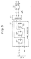
- Figure 5 is a detail circuit of the current-spare switching control unit shown in Fig. 3.
- 51 denotes a RS-type flip-flop circuit corresponding to the register 31 of Fig. 3
- 52 denotes a shift register corresponding to the shift register 32 of Fig. 3
- 53 denotes a decoder corresponding to the discrimination unit 33 of Fig. 3.
- the shift register 52 is constituted by D-type flip-flop circuits (52a to 52c).
- the shift command SC and the bits D1 to D3 are input from the internal microprocessor CPU of the fault supervisor 14 of Fig. 1.
- the bits D1 to D3 are sequentially input to the terminal D of the flip-flop circuit 52a.
- Each output of the flip-flop circuit 52a to 52c is input to the decoder 53.
- the decoder 53 decodes the bits D1 to D3 so that outputs bits "10" or "01" to the flip-flop circuit 51 produce the switching signal S.
Landscapes
- Engineering & Computer Science (AREA)
- Theoretical Computer Science (AREA)
- Quality & Reliability (AREA)
- Physics & Mathematics (AREA)
- General Engineering & Computer Science (AREA)
- General Physics & Mathematics (AREA)
- Hardware Redundancy (AREA)
- Storage Device Security (AREA)
Applications Claiming Priority (2)
| Application Number | Priority Date | Filing Date | Title |
|---|---|---|---|
| JP283044/90 | 1990-10-20 | ||
| JP2283044A JPH04156641A (ja) | 1990-10-20 | 1990-10-20 | レジスタアクセス装置 |
Publications (3)
| Publication Number | Publication Date |
|---|---|
| EP0482527A2 true EP0482527A2 (de) | 1992-04-29 |
| EP0482527A3 EP0482527A3 (en) | 1993-01-07 |
| EP0482527B1 EP0482527B1 (de) | 1996-05-08 |
Family
ID=17660488
Family Applications (1)
| Application Number | Title | Priority Date | Filing Date |
|---|---|---|---|
| EP91117830A Expired - Lifetime EP0482527B1 (de) | 1990-10-20 | 1991-10-18 | System zur Schaltsteuerung zwischen Normal und Ersatz |
Country Status (4)
| Country | Link |
|---|---|
| US (1) | US5218606A (de) |
| EP (1) | EP0482527B1 (de) |
| JP (1) | JPH04156641A (de) |
| DE (1) | DE69119351T2 (de) |
Families Citing this family (3)
| Publication number | Priority date | Publication date | Assignee | Title |
|---|---|---|---|---|
| KR930008680B1 (ko) * | 1991-05-15 | 1993-09-11 | 김덕우 | 이상검출표시 회로가 내장된 반도체 소자 |
| US5504859A (en) * | 1993-11-09 | 1996-04-02 | International Business Machines Corporation | Data processor with enhanced error recovery |
| US6157721A (en) | 1996-08-12 | 2000-12-05 | Intertrust Technologies Corp. | Systems and methods using cryptography to protect secure computing environments |
Family Cites Families (6)
| Publication number | Priority date | Publication date | Assignee | Title |
|---|---|---|---|---|
| GB1434186A (en) * | 1972-04-26 | 1976-05-05 | Gen Electric Co Ltd | Multiprocessor computer systems |
| ZA821999B (en) * | 1981-03-31 | 1983-05-25 | British Telecomm | Computor or processor control systems |
| US4823256A (en) * | 1984-06-22 | 1989-04-18 | American Telephone And Telegraph Company, At&T Bell Laboratories | Reconfigurable dual processor system |
| JP2700640B2 (ja) * | 1986-09-24 | 1998-01-21 | 日立超エル・エス・アイ・エンジニアリング 株式会社 | 半導体記憶装置 |
| FR2611401B1 (fr) * | 1987-02-26 | 1989-05-05 | Thomson Semiconducteurs | Procede de test d'adressage pour une memoire integree et dispositif de mise en oeuvre du procede |
| JPS63298888A (ja) * | 1987-05-29 | 1988-12-06 | Nippon Telegr & Teleph Corp <Ntt> | メモリアクセス方式 |
-
1990
- 1990-10-20 JP JP2283044A patent/JPH04156641A/ja active Pending
-
1991
- 1991-10-18 US US07/778,544 patent/US5218606A/en not_active Expired - Fee Related
- 1991-10-18 DE DE69119351T patent/DE69119351T2/de not_active Expired - Fee Related
- 1991-10-18 EP EP91117830A patent/EP0482527B1/de not_active Expired - Lifetime
Also Published As
| Publication number | Publication date |
|---|---|
| US5218606A (en) | 1993-06-08 |
| JPH04156641A (ja) | 1992-05-29 |
| EP0482527A3 (en) | 1993-01-07 |
| EP0482527B1 (de) | 1996-05-08 |
| DE69119351T2 (de) | 1996-10-10 |
| DE69119351D1 (de) | 1996-06-13 |
Similar Documents
| Publication | Publication Date | Title |
|---|---|---|
| US4701846A (en) | Computer system capable of interruption using special protection code for write interruption region of memory device | |
| US5301276A (en) | Method and device for assigning I/O address in data processing apparatus | |
| JPH04178114A (ja) | 電子機器 | |
| US5070476A (en) | Sequence controller | |
| US20040205384A1 (en) | Computer system and memory control method thereof | |
| US5218606A (en) | Current-spare switching control system | |
| US5446873A (en) | Memory checker | |
| EP0076098B1 (de) | Schlüsselspeicherfehlerverarbeitungssystem | |
| US6629262B1 (en) | Multiplexed storage controlling device | |
| EP0278528A2 (de) | Gebietsdurchsuchungssystem | |
| JPS59163653A (ja) | デバツグ装置 | |
| JPH0512131A (ja) | 情報処理装置 | |
| KR880001219B1 (ko) | 컴퓨터 오동작 방지 인터페이스 회로 | |
| JPS63129440A (ja) | ストアスル−バツフア装置 | |
| KR20040100724A (ko) | 외부 cpu의 잘못된 동작으로 인한 에러 제어 장치 및방법 | |
| JPH07152497A (ja) | ディスク制御装置 | |
| EP0112672A2 (de) | System zur Verarbeitung von Programmunterbrechung wegen eines Maschinenfehlers | |
| JP2892798B2 (ja) | ディジタル制御装置 | |
| JPH0395653A (ja) | データ記憶装置のアドレス誤り検出方法 | |
| KR950007107B1 (ko) | 별도의 마이크로프로세서를 포함하는 컴퓨터장치 | |
| JPS5899841A (ja) | 部分実装された制御メモリのアドレス制御方式 | |
| JP2727717B2 (ja) | プログラマブルコントローラシステム | |
| JPS63132356A (ja) | メモリバンク切換え装置 | |
| JPS62166449A (ja) | 論理装置の履歴記憶装置 | |
| JPH04364552A (ja) | パリティ監視回路付きメモリ回路 |
Legal Events
| Date | Code | Title | Description |
|---|---|---|---|
| PUAI | Public reference made under article 153(3) epc to a published international application that has entered the european phase |
Free format text: ORIGINAL CODE: 0009012 |
|
| AK | Designated contracting states |
Kind code of ref document: A2 Designated state(s): DE FR GB |
|
| RIN1 | Information on inventor provided before grant (corrected) |
Inventor name: YOSHIMURA, JUNICHI, C/O FUJITSU KYUSHU DIGITAL Inventor name: EGUCHI, YOSHITAKA, C/O FUJITSU KYUSHU DIGITAL |
|
| PUAL | Search report despatched |
Free format text: ORIGINAL CODE: 0009013 |
|
| AK | Designated contracting states |
Kind code of ref document: A3 Designated state(s): DE FR GB |
|
| 17P | Request for examination filed |
Effective date: 19930202 |
|
| 17Q | First examination report despatched |
Effective date: 19950728 |
|
| GRAH | Despatch of communication of intention to grant a patent |
Free format text: ORIGINAL CODE: EPIDOS IGRA |
|
| GRAA | (expected) grant |
Free format text: ORIGINAL CODE: 0009210 |
|
| AK | Designated contracting states |
Kind code of ref document: B1 Designated state(s): DE FR GB |
|
| PG25 | Lapsed in a contracting state [announced via postgrant information from national office to epo] |
Ref country code: FR Effective date: 19960508 |
|
| REF | Corresponds to: |
Ref document number: 69119351 Country of ref document: DE Date of ref document: 19960613 |
|
| EN | Fr: translation not filed | ||
| PG25 | Lapsed in a contracting state [announced via postgrant information from national office to epo] |
Ref country code: GB Effective date: 19961018 |
|
| PLBE | No opposition filed within time limit |
Free format text: ORIGINAL CODE: 0009261 |
|
| STAA | Information on the status of an ep patent application or granted ep patent |
Free format text: STATUS: NO OPPOSITION FILED WITHIN TIME LIMIT |
|
| 26N | No opposition filed | ||
| GBPC | Gb: european patent ceased through non-payment of renewal fee |
Effective date: 19961018 |
|
| PG25 | Lapsed in a contracting state [announced via postgrant information from national office to epo] |
Ref country code: DE Effective date: 19970701 |