EP0482564A2 - Verfahren zur Untersuchung einer Flüssigkristalltafel - Google Patents
Verfahren zur Untersuchung einer Flüssigkristalltafel Download PDFInfo
- Publication number
- EP0482564A2 EP0482564A2 EP19910117941 EP91117941A EP0482564A2 EP 0482564 A2 EP0482564 A2 EP 0482564A2 EP 19910117941 EP19910117941 EP 19910117941 EP 91117941 A EP91117941 A EP 91117941A EP 0482564 A2 EP0482564 A2 EP 0482564A2
- Authority
- EP
- European Patent Office
- Prior art keywords
- liquid crystal
- crystal panel
- histogram
- panel
- inspection method
- Prior art date
- Legal status (The legal status is an assumption and is not a legal conclusion. Google has not performed a legal analysis and makes no representation as to the accuracy of the status listed.)
- Withdrawn
Links
Images


Classifications
-
- G—PHYSICS
- G02—OPTICS
- G02F—OPTICAL DEVICES OR ARRANGEMENTS FOR THE CONTROL OF LIGHT BY MODIFICATION OF THE OPTICAL PROPERTIES OF THE MEDIA OF THE ELEMENTS INVOLVED THEREIN; NON-LINEAR OPTICS; FREQUENCY-CHANGING OF LIGHT; OPTICAL LOGIC ELEMENTS; OPTICAL ANALOGUE/DIGITAL CONVERTERS
- G02F1/00—Devices or arrangements for the control of the intensity, colour, phase, polarisation or direction of light arriving from an independent light source, e.g. switching, gating or modulating; Non-linear optics
- G02F1/01—Devices or arrangements for the control of the intensity, colour, phase, polarisation or direction of light arriving from an independent light source, e.g. switching, gating or modulating; Non-linear optics for the control of the intensity, phase, polarisation or colour
- G02F1/13—Devices or arrangements for the control of the intensity, colour, phase, polarisation or direction of light arriving from an independent light source, e.g. switching, gating or modulating; Non-linear optics for the control of the intensity, phase, polarisation or colour based on liquid crystals, e.g. single liquid crystal display cells
- G02F1/1306—Details
- G02F1/1309—Repairing; Testing
-
- Y—GENERAL TAGGING OF NEW TECHNOLOGICAL DEVELOPMENTS; GENERAL TAGGING OF CROSS-SECTIONAL TECHNOLOGIES SPANNING OVER SEVERAL SECTIONS OF THE IPC; TECHNICAL SUBJECTS COVERED BY FORMER USPC CROSS-REFERENCE ART COLLECTIONS [XRACs] AND DIGESTS
- Y10—TECHNICAL SUBJECTS COVERED BY FORMER USPC
- Y10S—TECHNICAL SUBJECTS COVERED BY FORMER USPC CROSS-REFERENCE ART COLLECTIONS [XRACs] AND DIGESTS
- Y10S345/00—Computer graphics processing and selective visual display systems
- Y10S345/904—Display with fail/safe testing feature
Definitions
- the present invention relates to a inspection method for liquid crystal panel used for a display device of a computer and so fourth.
- the defective products are found out by eye-inspection. First, observing the luminousness of the surface of a panel energized, the defective parts are roughly found out. Next, observing each part of a defective liquid crystal panel in detail, it is inspected where the defective parts are and how the parts are defective.
- Inspection method for automatic inspection of IC may be applicable to the inspection of liquid crystal.
- This method is one of a pattern matching method, in such an IC image is compared with a blueprint. Since the parts on the liquid crystal has a thickness and rather three-dimensional, the edge of the parts appears as shadowy lines, differently from the flat surface of IC.
- the input apparatus for the image of liquid crystal is adjusted not to take the shadowy lines, however a part of the lines may be inputted due to optical aberration. In such an image, it is impossible to find out defective parts without fail by comparing the parts with a template.
- the present invention is invented to provide a liquid crystal panel inspection method, by which it is possible for the unskilled to inspect whole of a liquid crystal panel accurately in a short time.
- the liquid crystal panel inspection method according to the present invention is characterized in that a part is selected as a reference image in the parts group maximal number of members among groups classified according to characteristics value, then other parts to be extracted are compared with the reference part.
- the liquid crystal panel inspection method according to the present invention is further characterized in that the judgment whether a part to be inspected has a defect or not is performed by comparing images of a liquid crystal panel to be inspected with a part image of no defect, observing the images by lighting from backside of them.
- the liquid crystal panel inspection method according to the present invention is further characterized in that a liquid crystal panel to be inspected is inputted optically and is judged if it has a defect or not according to a characteristics of a histogram of the part.
- FIG. 3 shows an apparatus used for the present invention.
- a liquid crystal panel 11 is located inside of a support frame 12 so as to be fixed on the frame 12 with bolts 13.
- Support frame 12 movably mounted on a pair of rails 15 on a movable plate 14.
- a cylinder device 16 is fixed on an end of the movable plate 14, whose piston rod 17 is connected with the support frame 12.
- Movable plate 14 is movably mounted on a pair of rails 22 on fixed plate 21.
- the fixed plate 21 is provided with a cylinder device 23 at one end whose piston rod 24 is connected with the movable plate 14.
- Support frame 12 is moved in parallel to movable frame 14 by controlling cylinder device 16, and movable plate 14 is moved in parallel to fixed plate 21 by controlling cylinder device 23.
- Cylinder devices 16 and 23 are driven by drive circuits 25 and 26, respectively, so as to move the piston rods 17 and 24 forward or backward.
- Drive circuits 25 and 26 are controlled by a control circuit 27.
- a microscope 31 is supported by a fixed frame not shown above the liquid crystal panel 11. Each part equipped on liquid crystal panel 11 is inputted through the microscope 31, as described later. The image of this part is inputted to image processing system 32 and various processings are performed therein. Image processing system 32 is controlled by computer 33.
- Light sources 34 and 35 are provided for lighting the support frame 12 from above and below, respectively. They are fixed to support frame 12 and move with it. Light sources 34 and 35 are driven by a drive circuit 36 which is controlled by the control circuit 27.
- liquid crystal panel 11 includes a plurality of parts 41 mounted and arranged regularly on the panel. Each part 41 is driven to emit light by a voltage supplied through leads 42 and 43.
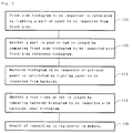
- Fig. 1 and Fig. 2 show an inspection method for finding such a defect.
- Fig. 1 shows the outline of inspection process and
- Fig. 2 shows details of the step 106 in Fig. 1.
- the liquid crystal panel is measured which has already been inspected which to be assured of defectlessness.
- the liquid crystal panel after the inspection is mounted on the inspection system in Fig. 3.
- a liquid crystal panel is photographed by lighting from front side of it and the image of a part is inputted into image processing system 32.
- Image processing system 32 cooperates with a computer 33 to calculate the brightness of each pixel of inputted image with 256 monochrome densities and a histogram of each density is obtained by calculating the number of pixels of each density.
- This histogram is called front side ideal histogram here.
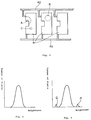
- the front side ideal histogram shows the brightness distribution of a part of inspected liquid crystal panel, having one peak as shown in Fig. 5. The most number of pixels belongs to the predetermined brightness and less number of pixels belongs to higher or lower brightness than the predetermined brightness as it follows.
- step 102 lighting inspected liquid crystal panel from backside, an image of a liquid crystal panel is inputted to image processing system 32.
- image processing system 32 As the image is not a part but a whole of liquid crystal panel, a video camera is used in place of microscope 31.
- Image processing system 32 and computer 33 are used for calculating the histogram of brightness distribution of an inputted image. This histogram is called an backside ideal histogram here.
- the backside ideal histogram is a distribution of brightness when an inspected liquid crystal panel is lighted from backside. Since leads 42 and 43 of an inspected liquid crystal panel do not rise from the panel, light do not pass through the panel. Therefore, a lot of pixels belongs to low brightnesses.
- Steps from 103 to 106 are for the measurement and judgment of the liquid crystal panel if it is defective or not.
- This liquid crystal panel to be inspected is mounted on the inspection system in Fig. 3.
- step 103 lighting from front side and photographing a liquid crystal panel to be inspected, an image of a part is inputted to image processing system 32.
- a histogram of brightness distribution is calculated with observing each pixel of the image.
- a part belonging to a major group in classification of characteristics is selected as a reference part by calculating such a histogram and by comparing the histograms with one another.
- the reference part is decided by a majority. For example, the one which belongs to the group with the maximal number of similar histograms is decided as a reference part.
- the histogram of the reference part is registered in the memory of computer 33 as the front side reference histogram in step 104.
- step 105 comparing the front side reference histogram registered on step 104 with the front side ideal histogram calculated on step 101, the liquid crystal panel to be inspected is judged to be defectless in all-over when the histograms are similar to each other.
- the "all-over defect” means the discolored into black-burned part with roughness, or light blot generated by peeling off of protect film from a panel. When such defects exist, the histograms of them show many pixels on low brightness, or wide distribution on a lot of brightnesses.
- step 105 when an all-over defect is found out on a panel to be inspected, the inspection process is terminated here. When such a defect is not found out, each part of the liquid crystal panel to be inspected is judged the quality on step 106.
- Fig. 2 shows the processing in step 106 in detail.
- Step 111 and 112 judge the existence of a break A, a big hole B and pin point C (such as in Fig. 4), which are executed one by one to all the parts of a liquid crystal panel to be inspected.
- liquid crystal panel 11 is controlled its location by cylinder device 16 and 23 for predetermined part of it to be just under microscope 31, as shown in Fig. 3, every time steps 111 and 112 are executed.
- a panel to be inspected is lighted from the front side and photographed, and an image of a part is inputted to image processing system 32.
- Image processing system 32 and computer 33 calculate the histogram of brightness distribution of inputted image in the same way as in step 101.
- This histogram is called "histogram to be inspected on the front side".
- the histogram to be inspected on the front side shows a simple wavy line with one peak as shown in Fig. 5.
- a defect such as break A or big hole B exists
- light reflects at the defects because of the bareness of the panel. It causes a peak of histogram of high brightness as shown by "P” in Fig. 6.
- the part of pin point C shows black shadow. It causes a peak of histogram on low brightness as shown by "Q" in Fig. 6.
- step 112 comparing the histogram to be inspected on the front side calculated on step 111 with the reference histogram on the front side, the part is judged to be defectless when their histogram are similar to each other.
- the defect which can be inspected on this step are break A, big hole B and pin point C described above.
- step 112 the existence of such defects is inspected by recognizing the peak of histogram shown by "P" or "Q" in Fig. 6.
- Various methods are possible for the comparison of histogram to be inspected on the front side and the reference histogram on the front side, similarly to the comparison on step 105.
- the methods consists of steps of i) to compare the difference of pixels on each brightness with the threshold after subtracting each histogram, ii) to compare the secondary moments of each histogram, iii) to compare the distribution of brightness calculated from each histogram.
- step 112 the reference histogram on the front side which is a characteristics value of an image of a reference part is compared with the histogram to be inspected on the front side which is a characteristics value of an image of a part to be inspected.
- the part to be inspected is judged to be defectless or not.
- Steps 113 and 114 are judgment of the existence of rising leads 42 and 43 from the panel, which are executed by lighting from the back side of a liquid crystal panel to be inspected.
- Liquid crystal panel 11 is lighted by lighting source 35 below it, as shown in Fig. 3, and taken a movie by a video camera equipped in place of microscope 31.
- the histogram of brightness distribution is calculated after inputting the image whole of liquid crystal panel into image processing system 32 lighted from backside of the panel to be inspected.
- the histogram is called "backside histogram to be inspected".
- the histogram has high peak on low brightness because the panel is opaque to the light from backside substantially.
- the histogram has peak on high brightness because the light lighted from backside passes through the part.
- step 114 backside histogram to be inspected is compared with the ideal histogram of backside calculated in step 102.
- leads 42 and 43 are judged not risen from the liquid crystal panel to be inspected.
- a backside histogram to be inspected has high peak on high brightness, and the backside histogram to be inspected and the ideal histogram of backside are not similar to each other, it is judged that leads 42 or 43 rise from the panel on some part of liquid crystal panel to be inspected.
- step 115 the results of the inspection above are registered to the memory of computer 33.
- the result of the inspection can be seen on a display which is not shown in the figure.
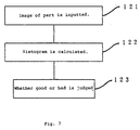
- Fig. 7 shows the method for judging if the part is defectless or not by the characteristic of the histogram inputted optically, without inputting the reference part.
- step 121 lighting and photographing the part of a liquid crystal panel to be inspected, the image of a part is inputted to image processing system 32.
- step 122 image processing is performed to the part and the histogram is calculated.
- step 123 the part is judged if it is defectless or not according to the characteristic of the histogram.
- the reference histogram is obtained from a part selected in the major group: the histogram can be obtained by calculating a mean value or other statistics value of histograms of the parts of the group selected.
Landscapes
- Physics & Mathematics (AREA)
- Nonlinear Science (AREA)
- Chemical & Material Sciences (AREA)
- Crystallography & Structural Chemistry (AREA)
- General Physics & Mathematics (AREA)
- Optics & Photonics (AREA)
- Investigating Materials By The Use Of Optical Means Adapted For Particular Applications (AREA)
- Testing Of Optical Devices Or Fibers (AREA)
- Length Measuring Devices By Optical Means (AREA)
- Image Processing (AREA)
- Liquid Crystal (AREA)
Applications Claiming Priority (2)
| Application Number | Priority Date | Filing Date | Title |
|---|---|---|---|
| JP2283760A JPH04158238A (ja) | 1990-10-22 | 1990-10-22 | 液晶パネルの検査方法 |
| JP283760/90 | 1990-10-22 |
Publications (2)
| Publication Number | Publication Date |
|---|---|
| EP0482564A2 true EP0482564A2 (de) | 1992-04-29 |
| EP0482564A3 EP0482564A3 (en) | 1992-09-23 |
Family
ID=17669764
Family Applications (1)
| Application Number | Title | Priority Date | Filing Date |
|---|---|---|---|
| EP19910117941 Withdrawn EP0482564A3 (en) | 1990-10-22 | 1991-10-21 | Liquid crystal panel inspection method |
Country Status (4)
| Country | Link |
|---|---|
| US (1) | US5204617A (de) |
| EP (1) | EP0482564A3 (de) |
| JP (1) | JPH04158238A (de) |
| KR (1) | KR920008519A (de) |
Cited By (2)
| Publication number | Priority date | Publication date | Assignee | Title |
|---|---|---|---|---|
| EP0573045A3 (de) * | 1992-06-03 | 1995-02-22 | Casio Computer Co Ltd | LCD mit Photosensor. |
| EP0672933A1 (de) * | 1994-03-14 | 1995-09-20 | Orbotech Ltd | Vorrichtung und Verfahren zur Inspektion einer Anzeigetafel |
Families Citing this family (15)
| Publication number | Priority date | Publication date | Assignee | Title |
|---|---|---|---|---|
| EP0495481A3 (en) * | 1991-01-16 | 1993-06-02 | Ezel Inc. | Liquid crystal panel inspection method |
| US5404111A (en) * | 1991-08-03 | 1995-04-04 | Tokyo Electron Limited | Probe apparatus with a swinging holder for an object of examination |
| US5391985A (en) * | 1992-03-06 | 1995-02-21 | Photon Dynamics, Inc. | Method and apparatus for measuring high speed logic states using voltage imaging with burst clocking |
| US5754678A (en) * | 1996-01-17 | 1998-05-19 | Photon Dynamics, Inc. | Substrate inspection apparatus and method |
| JP3333686B2 (ja) * | 1996-06-28 | 2002-10-15 | 松下電器産業株式会社 | 表示画面検査方法 |
| US5754305A (en) * | 1996-12-03 | 1998-05-19 | Eastman Kodak Company | Method and apparatus for correcting light non-uniformity in an LCD photographic printer |
| US5870205A (en) * | 1996-12-03 | 1999-02-09 | Eastman Kodak Company | Method and apparatus for correcting light non-uniformity in an LCD photographic printer |
| US6714670B1 (en) * | 1998-05-20 | 2004-03-30 | Cognex Corporation | Methods and apparatuses to determine the state of elements |
| US6219443B1 (en) * | 1998-08-11 | 2001-04-17 | Agilent Technologies, Inc. | Method and apparatus for inspecting a display using a relatively low-resolution camera |
| US6765203B1 (en) * | 2003-01-31 | 2004-07-20 | Shimadzu Corporation | Pallet assembly for substrate inspection device and substrate inspection device |
| TW594655B (en) * | 2003-07-11 | 2004-06-21 | Toppoly Optoelectronics Corp | Testing circuit and method thereof for a flat panel display |
| KR20060073741A (ko) * | 2004-12-24 | 2006-06-29 | 삼성전자주식회사 | 응답속도 측정장치와 이를 이용한 응답속도 측정방법 |
| WO2008136067A1 (ja) * | 2007-04-20 | 2008-11-13 | Meinan Machinery Works, Inc. | 木材の検査方法及び装置及びプログラム |
| CN104570422B (zh) * | 2014-12-31 | 2017-10-13 | 深圳市华星光电技术有限公司 | 一种液晶显示面板的品质的监控方法 |
| TWI793035B (zh) * | 2022-06-24 | 2023-02-11 | 晶睿通訊股份有限公司 | 影像缺陷辨識方法及其影像分析裝置 |
Family Cites Families (5)
| Publication number | Priority date | Publication date | Assignee | Title |
|---|---|---|---|---|
| US4589139A (en) * | 1982-02-04 | 1986-05-13 | Nippon Kogaku K. K. | Apparatus for detecting defects in pattern |
| DE3683053D1 (de) * | 1986-10-23 | 1992-01-30 | Ibm | Verfahren zur kontaktfreien pruefung von platinen fuer integrierte schaltungen unter atmosphaerischen bedingungen. |
| US4819038A (en) * | 1986-12-22 | 1989-04-04 | Ibm Corporation | TFT array for liquid crystal displays allowing in-process testing |
| NL8700933A (nl) * | 1987-04-21 | 1988-11-16 | Philips Nv | Testmethode voor lcd-elementen. |
| US5057775A (en) * | 1990-05-04 | 1991-10-15 | Genrad, Inc. | Method of testing control matrices for flat-panel displays |
-
1990
- 1990-10-22 JP JP2283760A patent/JPH04158238A/ja active Pending
-
1991
- 1991-10-21 US US07/780,053 patent/US5204617A/en not_active Expired - Fee Related
- 1991-10-21 EP EP19910117941 patent/EP0482564A3/en not_active Withdrawn
- 1991-10-21 KR KR1019910018515A patent/KR920008519A/ko not_active Ceased
Cited By (5)
| Publication number | Priority date | Publication date | Assignee | Title |
|---|---|---|---|---|
| EP0573045A3 (de) * | 1992-06-03 | 1995-02-22 | Casio Computer Co Ltd | LCD mit Photosensor. |
| US5446564A (en) * | 1992-06-03 | 1995-08-29 | Casio Computer Co., Ltd. | Liquid crystal display device having photosensor at each pixel |
| EP0672933A1 (de) * | 1994-03-14 | 1995-09-20 | Orbotech Ltd | Vorrichtung und Verfahren zur Inspektion einer Anzeigetafel |
| US5771068A (en) * | 1994-03-14 | 1998-06-23 | Orbotech Ltd. | Apparatus and method for display panel inspection |
| US6215895B1 (en) | 1994-03-14 | 2001-04-10 | Orbotech Ltd. | Apparatus and method for display panel inspection |
Also Published As
| Publication number | Publication date |
|---|---|
| KR920008519A (ko) | 1992-05-28 |
| JPH04158238A (ja) | 1992-06-01 |
| EP0482564A3 (en) | 1992-09-23 |
| US5204617A (en) | 1993-04-20 |
Similar Documents
| Publication | Publication Date | Title |
|---|---|---|
| US5204617A (en) | Liquid crystal panel inspection method | |
| EP3531114B1 (de) | Vorrichtung zur visuellen inspektion und verfahren zur einstellung der beleuchtungsbedingung einer visuellen inspektionsvorrichtung | |
| US5339093A (en) | Liquid crystal panel inspection method | |
| US7868644B2 (en) | Apparatus and method for inspecting liquid crystal display | |
| US6661912B1 (en) | Inspecting method and apparatus for repeated micro-miniature patterns | |
| US20250029280A1 (en) | System and method for determining whether a camera component is damaged | |
| CN115165920B (zh) | 一种三维缺陷检测方法及检测设备 | |
| US5995680A (en) | Cytological system illumination integrity checking apparatus and method | |
| CN115493843A (zh) | 一种基于轴承保持器的质量监测方法及设备 | |
| US7800568B2 (en) | Apparatus and method for inspecting liquid crystal display | |
| CN115546140A (zh) | 一种显示面板检测方法、系统及电子装置 | |
| EP0495481A2 (de) | Verfahren zur Untersuchung einer Flüssigkristalltafel | |
| CN100538347C (zh) | 膜式或带式印制电路板的自动光学检测系统及处理方法 | |
| JP2002303581A (ja) | パネル検査装置及びパネル検査方法 | |
| JP3314217B2 (ja) | 外観検査装置 | |
| Affolder et al. | Automated visual inspection and defect detection of large-scale silicon strip sensors | |
| KR100591853B1 (ko) | Lcd 모듈 검사 방법 및 장치 | |
| KR100249597B1 (ko) | 광학적 불균일 검사장치 및 광학적 불균일 검사방법 | |
| CN116071356B (zh) | 用于设计企业的设计图缺陷智慧检查平台及检查方法 | |
| CN116228662B (zh) | 检测方法及装置、检测设备和计算机可读存储介质 | |
| JPH10206344A (ja) | 光学的むら検査装置および光学的むら検査方法 | |
| KR100249598B1 (ko) | 광학적 불균일 검사장치 및 광학적 불균일 검사방법 | |
| KR20060008609A (ko) | 웨이퍼 검사 방법 | |
| CN121186070A (zh) | 一种在线检测试纸条和基板外观缺陷的光学系统及方法 | |
| CN121933537A (zh) | Micro-LED屏幕缺陷检测系统和方法 |
Legal Events
| Date | Code | Title | Description |
|---|---|---|---|
| PUAI | Public reference made under article 153(3) epc to a published international application that has entered the european phase |
Free format text: ORIGINAL CODE: 0009012 |
|
| AK | Designated contracting states |
Kind code of ref document: A2 Designated state(s): DE FR GB |
|
| PUAL | Search report despatched |
Free format text: ORIGINAL CODE: 0009013 |
|
| AK | Designated contracting states |
Kind code of ref document: A3 Designated state(s): DE FR GB |
|
| 17P | Request for examination filed |
Effective date: 19920901 |
|
| RAP1 | Party data changed (applicant data changed or rights of an application transferred) |
Owner name: EZEL INC. Owner name: SHARP KABUSHIKI KAISHA |
|
| RAP1 | Party data changed (applicant data changed or rights of an application transferred) |
Owner name: EZEL INC. Owner name: SHARP KABUSHIKI KAISHA |
|
| RAP3 | Party data changed (applicant data changed or rights of an application transferred) |
Owner name: EZEL INC. Owner name: SHARP KABUSHIKI KAISHA |
|
| 17Q | First examination report despatched |
Effective date: 19940826 |
|
| STAA | Information on the status of an ep patent application or granted ep patent |
Free format text: STATUS: THE APPLICATION IS DEEMED TO BE WITHDRAWN |
|
| 18D | Application deemed to be withdrawn |
Effective date: 19950307 |