EP0482828B1 - Interface de commande spécifique pour des messages - Google Patents
Interface de commande spécifique pour des messages Download PDFInfo
- Publication number
- EP0482828B1 EP0482828B1 EP91309605A EP91309605A EP0482828B1 EP 0482828 B1 EP0482828 B1 EP 0482828B1 EP 91309605 A EP91309605 A EP 91309605A EP 91309605 A EP91309605 A EP 91309605A EP 0482828 B1 EP0482828 B1 EP 0482828B1
- Authority
- EP
- European Patent Office
- Prior art keywords
- byte
- data
- message
- register
- signal
- Prior art date
- Legal status (The legal status is an assumption and is not a legal conclusion. Google has not performed a legal analysis and makes no representation as to the accuracy of the status listed.)
- Expired - Lifetime
Links
- 230000002093 peripheral effect Effects 0.000 claims description 42
- 230000005540 biological transmission Effects 0.000 claims description 8
- 230000008878 coupling Effects 0.000 claims 1
- 238000010168 coupling process Methods 0.000 claims 1
- 238000005859 coupling reaction Methods 0.000 claims 1
- 238000012546 transfer Methods 0.000 description 10
- 238000004891 communication Methods 0.000 description 9
- 230000006870 function Effects 0.000 description 8
- 238000010586 diagram Methods 0.000 description 4
- 230000002457 bidirectional effect Effects 0.000 description 3
- 230000001360 synchronised effect Effects 0.000 description 3
- 238000001514 detection method Methods 0.000 description 2
- 238000012360 testing method Methods 0.000 description 2
- 238000013497 data interchange Methods 0.000 description 1
- 230000001419 dependent effect Effects 0.000 description 1
- 238000011161 development Methods 0.000 description 1
- 230000000694 effects Effects 0.000 description 1
- 238000005516 engineering process Methods 0.000 description 1
- 230000008520 organization Effects 0.000 description 1
- 238000012545 processing Methods 0.000 description 1
- 239000007787 solid Substances 0.000 description 1
Images


Classifications
-
- H—ELECTRICITY
- H04—ELECTRIC COMMUNICATION TECHNIQUE
- H04L—TRANSMISSION OF DIGITAL INFORMATION, e.g. TELEGRAPHIC COMMUNICATION
- H04L51/00—User-to-user messaging in packet-switching networks, transmitted according to store-and-forward or real-time protocols, e.g. e-mail
- H04L51/21—Monitoring or handling of messages
-
- H—ELECTRICITY
- H04—ELECTRIC COMMUNICATION TECHNIQUE
- H04L—TRANSMISSION OF DIGITAL INFORMATION, e.g. TELEGRAPHIC COMMUNICATION
- H04L12/00—Data switching networks
- H04L12/28—Data switching networks characterised by path configuration, e.g. LAN [Local Area Networks] or WAN [Wide Area Networks]
- H04L12/40—Bus networks
- H04L12/407—Bus networks with decentralised control
- H04L12/417—Bus networks with decentralised control with deterministic access, e.g. token passing
-
- H—ELECTRICITY
- H04—ELECTRIC COMMUNICATION TECHNIQUE
- H04L—TRANSMISSION OF DIGITAL INFORMATION, e.g. TELEGRAPHIC COMMUNICATION
- H04L9/00—Cryptographic mechanisms or cryptographic arrangements for secret or secure communications; Network security protocols
- H04L9/40—Network security protocols
Definitions
- This invention relates to message-oriented digital communication, such as that which can be utilized between a Bank Controller Unit and peripheral devices.
- digital transmission occurs between a central office terminal and a remote terminal, and between a remote terminal and the subscribers.
- the various units of the remote terminal such as channel units, are controlled by a Bank Controller Unit which communicates with the various peripheral units through a register-oriented interface.
- US-A-4 071 887 discloses a synchronous data adaptor which provides a bidirectional interface for synchronous data interchange.
- Internal control and interface logic including first-in-first-out buffer memory enable simultaneous transmitting and receiving of standard synchronous communication characters to allow data transfer between serial data channels and the parallel bidirectional data bus of a bus organised system such as a microprocessor system.
- An embodiment described below is a circuit for transmitting and receiving a digital data stream including multiple bytes of data and control signals, where the circuit comprises at least four registers.
- a first register is adapted to receive control signals which are part of the digital stream, while a second register is adapted to transmit control signals as part of the digital stream.
- a third register is adapted to receive data which is part of the digital stream, while a fourth register is adapted to transmit data as part of the digital stream.
- a fifth register may also be included to store data transmitted by the fourth register and to transmit the data in the event of an error in transmitting the data from the fourth register.
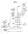
- FIG. 1 is a block diagram illustrating a typical Bank Controller Unit link to peripheral devices in the central office terminal or remote terminal of a digital loop transmission system.
- the Bank Controller Unit (BCU), 10, includes a microprocessor, 11, which communicates to a Serial Control Link Driver (SCLD), 12, which is usually part of an Alarm and Display Unit (ADU), 13. Communication takes place over a Data/Address (D/A) bus 28.
- the Serial Control Link Driver, 12 communicates with each Bank Peripheral Device (BPD), such as 14, by means of two sets of leads, designated NP and NQ leads, 15 and 16, respectively, as well as a bidirectional serial data bus 17.
- BPD Bank Peripheral Device
- One NP lead, one NQ lead and the data bus terminate on a Bank Control Link Terminator, e.g., 18, which is part of each peripheral device's circuitry.
- the NP and NQ leads jointly select the peripheral device, while the data pass over the data bus in both directions.
- the terminator includes registers (not shown) which can be accessed by the peripheral device's microprocessor 19.
- Each peripheral device, 14, also has a service request (SR) lead, 20, which is coupled directly to the Bank Controller Unit, 10, and which is shared among several peripheral devices.
- SR service request
- This lead can provide an interrupt function during the normal BCU communication with the peripheral device.
- the BCU, 10 would command the SCLD, 12, to send a message typically containing eight bits of data to a specified register of a peripheral device.
- the SCLD would then send the message to the terminator of the peripheral device, 14, as further illustrated in FIG. 4 along with the waveforms of the NP and NQ leads to that peripheral device.
- the message consisted of a read/write select bit, 16 message bits and a parity bit.
- the 16 message bits, as shown, were, typically, divided into an address field (A 0 - A 7 ) that identified the register designated to receive the message, and a data field (D 0 - D 7 ) that contained the data to be written into the register.
- the peripheral device would send back two check code bits (C 0 - C 1 ) to indicate whether received and calculated parity agreed and whether the register address was valid.
- SCLD Serial Control Link Driver
- the peripheral device would send back two check code bits (C 0 - C 1 ), 16 message bits, and a parity bit (P).
- the message bits would be divided into an address field (A 0 - A 7 ) that identified the register being read and a data field (D 0 - D 7 ) containing the data in that register.
- the SCLD would also test for a match between received and calculated parity. After each read and write operation, the BCU would read a register on the SCLD, which register's content would indicate whether the operation was error-free. In the case of an error-free read operation, the BCU would read yet another register in the SCLD, which register would contain the data obtained from the peripheral device. If an error were reported, the BCU would try again. For additional error protection on a read operation, the BCU would compare the address register information in the messages transmitted and received by the SCLD.
- each peripheral device is provided with at least four, and preferably five, registers which are dedicated to message-oriented communication with that device, as illustrated in the block diagram of FIG. 2.
- Each register, 21-25, in this example is 8-bits wide.
- the register, 21, labeled "SIG_OUT”, receives outgoing control signals, while the register, 22, labeled "DATA_OUT” receives outgoing message data.
- Outgoing refers to communication from the BCU toward the peripheral device, while "Incoming” denotes communication from the peripheral device to the BCU.) Incoming communication is handled by three registers.
- Register, 23, labeled “SIG_IN” receives control signals from the peripheral device, while register, 24, labeled “DATA_IN1” receives the data messages.
- the final, optional, register, 25, labeled “DATA_IN2” holds the last byte read by the SCLD from "DATA_IN1". In case there is an error, this byte can then be re-read by the SCLD from this auxiliary register.
- Control circuitry, 26 and 27, provides several functions including selecting a register, deciding whether the chosen register is to be read or written, determining whether an error has occurred in transmission from the BCU, and notifying the BCU or peripheral device's microprocessor whether a transmission error has occurred. Notifying the BCU of an error in an outgoing message can be accomplished by controlling the value of the check code, previously mentioned.
- the peripheral device Whenever the SIG_IN register, 23, contains a control signal value other than IDLE, the peripheral device will assert a service request toward the BCU on the service request lead, 20. This feature enables the BCU to recognize a pending information transfer without periodically polling the SIG_IN registers, which polling would divert a portion of the BCU's processing capacity from other tasks.
- a signal value of IDLE in the SIG_IN register causes the service request to be retired. In this example, the IDLE value is zero.
- flow control is implemented by using a new value of the check code.
- Flow control ensures that the BCU does not send or receive data faster than the peripheral device can receive or send the data, respectively.
- the BCU should not write a byte into the BPD's DATA_OUT register until the peripheral device's microprocessor (19) has copied the previous byte from DATA_OUT, and the BCU should not read the BPD's DATA_IN1 register while it contains data previously read by the BCU or the DATA_IN2 register while it does not contain current data.
- the check code will indicate that the register is BUSY.
- the terminator will send out a newly designated value of the existing two-bit check code to indicate this fact to the BCU. That is, the newly designated value of ⁇ 1,1 ⁇ indicates a good parity, a valid register address, but a busy data register.
- FIG. 3 illustrates the message format utilized in accordance with the invention.
- the message is transferred from the BCU to the peripheral device via the DATA_OUT register, 22, or from the peripheral device to the BCU via the DATA_IN1 and DATA_IN2 registers, 24 and 25, respectively.
- Each division indicates one byte of the message.
- the first two bytes, 31 and 32, labeled “Length (Lower)” and “Length (Upper)” indicate to the receiver the total length of the message, including the length bytes themselves and the Stop and Checksum bytes (40 and 41, respectively).
- the Length (Lower) byte contains the least significant eight bits of the binary number representing the length.
- the Length (Upper) byte contains the most significant eight bits of the number representing the length.
- the Physical Target (Coarse) byte, 33 designates the particular central office or remote terminal to which the message will be sent.
- the Physical Target (Fine) byte, 34 indicates the particular circuit card in the central office or remote terminal to which the message will be sent.
- the Firmware Target (Coarse) byte, 35 designates the broad category of firmware or software which will receive the message (e.g., the firmware which handles inventory control), while the Firmware Target (Fine) byte, 36, indicates the specific function of the destination firmware object (e.g., the function of accepting inventory information from a peripheral device).
- the Physical Source (Coarse) byte, 37 designates the central office or remote terminal from which the message is transmitted, while the Physical Source (Fine) byte indicates the circuit card within the central office or remote terminal from which the message originates.
- the above-described header bytes are followed by the Information bytes, 39, which contain the payload of the message (i.e., the block of data whose transfer is the ultimate purpose of the invention). It is contemplated that the Information portion of the message may have any length from zero to 65,525 bytes, and can have any content, since the data and control signals will be handled by different registers.
- the Information is followed by a Stop byte, 40, with a fixed value. This byte serves as part of the error detection capability of the system by verifying that the number of bytes received in the message is equal to the number of bytes promised in the Length bytes (31 and 32). The remainder of the error detection capability is provided by the Checksum byte 41.
- Each bit in the Checksum byte is the exclusive OR function of the corresponding bits in all the bytes previously received in the message starting with Length byte 31 and ending with Stop byte 40.
- the exclusive OR function will be calculated for each of the other bits in the Checksum byte.
- Stop and Checksum bytes are particularly useful in digital loop systems since the peripheral devices tend to have small (8-bit) processors and limited memory space (typically less than 256 bytes of RAM and less than 4 Kbytes of ROM). Further, the use of the Stop byte in addition to the Checksum byte is desirable for reducing still further the probability of failing to detect an error in the length bytes.
- Table I below indicates in more detail a typical message transfer from the Bank Controller Unit (BCU) to the Bank Peripheral Device (BPD).
- the first column designates the function performed by the BCU, the second column designates the register employed, and the third column designates the function performed by the BPD.
- the arrows between columns illustrate the direction of transfer of the control signal bytes and data bytes.
- the solid double arrow indicates a service request asserted by the BPD, while the dotted double arrow indicates retiring of a service request.
- the BCU first writes a Request to Send (RTS) signal into the SIG_OUT register (see FIG. 2) which is read by the BPD.
- the BPD then writes a Clear to Send (CTS) signal into the SIG_IN register which is read by the BCU.
- CTS Clear to Send
- SMO Start of Message Out
- IDLE Idle signal
- the BCU then writes the data bytes (31 to 41 inclusive in FIG. 3) one byte at a time into the DATA_OUT register, where they are read out one byte at a time by the BPD.
- the BPD If, at any time, the BPD responds to an offered byte with a busy check code, the BCU saves the byte and tries again later. After the last (Checksum) byte is read, the BPD compares the Checksum byte with the checksum that the BPD has calculated as it received the message. Assuming no errors are present, the BPD acknowledges the message to the BCU by writing Message Acknowledge (MACK) in the SIG_IN register. The BCU then indicates the End of Message in the SIG_OUT register, and the BPD retires the service request by writing an Idle signal in the SIG_IN register.
- MACK Message Acknowledge
- BPD_BSY BPD Busy
- Table II illustrates a typical message transfer from the BPD to the BCU.
- the BPD begins by writing the first data byte into both the DATA_IN1 and DATA_IN2 registers.
- the BPD then writes a Request to Send signal into the SIG_IN register where it is read by the BCU.
- the BCU responds by writing a Start of Message In signal into the SIG_OUT register which is read by the BPD.
- An Idle signal is then sent by the BPD to retire the service request.
- the BCU then reads the first Data byte which was previously written into the DATA_IN1 register. Subsequently, the BPD writes the remainder of the Data bytes, one byte at a time, into the DATA_IN1 register.
- the BPD will copy the new byte into DATA_IN2.
- the BCU reads the Data bytes from DATA_IN1 as they are written therein, and, if an error is detected, will re-read a byte from DATA_IN2. If a Data byte in DATA_IN2 is not read, it will merely be replaced by the next byte.
- the BCU After reading the last byte, the BCU will compare the Checksum byte with the checksum that the BCU has calculated as it received the message, and, if there is agreement, send a message acknowledgment by writing Message Acknowledge (MACK) into the SIG_OUT register.
- MACK Message Acknowledge
- this byte transfer protocol permits a message of any length from 10 to 65,535 bytes containing from zero to 65,525 Information bytes, and in no way restricts the content of an Information byte.
- either the BCU or BPD can abort by issuing an appropriate signal, i.e., the sender can issue an End of Message (EOM) signal or the receiver can issue a Message Transmit Abort (MTA) signal.
- EOM End of Message
- MTA Message Transmit Abort
- the receiver of a message If the receiver of a message detects a wrong value in the STOP byte, or finds a checksum disagreement, the receiver sends a "Message Transmission Error" (MTE) signal to the sender via the SIG_IN or SIG_OUT register, as appropriate. The sender may then re-transmit the message.
- MTE Message Transmission Error
Landscapes
- Engineering & Computer Science (AREA)
- Computer Networks & Wireless Communication (AREA)
- Signal Processing (AREA)
- Computer Security & Cryptography (AREA)
- Communication Control (AREA)
- Small-Scale Networks (AREA)
- Information Transfer Systems (AREA)
- Computer And Data Communications (AREA)
Claims (8)
- Circuit dans un périphérique de groupe destiné à être utilisé dans un système de transmission à boucle numérique, ledit circuit étant adapté pour transmettre et recevoir des trains numériques comportant des messages de données à octets multiples et des signaux de commande sur une liaison de contrôleur de groupe comprenant un bus de données unique entre le périphérique et un contrôleur de groupe dans ladite boucle dans lequel les messages de données comprennent une pluralité d'octets d'en-tête, une pluralité d'octets d'information, un octet d'Arrêt et un octet de Total de Contrôle, chaque octet comportant un certain nombre de positions de bits, l'octet de Total de Contrôle comprenant des bits qui sont une fonction OU exclusif de tous les bits dans la même position de bit dans les octets précédents du message de données, ledit circuit étant CARACTERISE PARun premier circuit de commande (26) adapté pour être couplé au bus de données et pour transmettre des messages à octets multiples dans un mode de transmission et recevoir des messages à octets multiples dans un mode de réception de telle sorte que les messages de données et les signaux de commande soient transmis et reçus sur le bus de données unique ;un premier registre (21) couplé électriquement au premier circuit de commande et adapté pour recevoir un signal de "demande pour émettre", un signal de "début de message sortant" et un signal de "fin de message" à partir du bus de données dans le mode de réception et recevoir un signal de début de message entrant et un signal d'accusé de réception de message dans le mode de transmission ;un deuxième circuit de commande (27) ;un deuxième registre (23) couplé électriquement audit deuxième circuit de commande et adapté pour transmettre un signal "prêt à émettre" et un signal d'accusé de réception de message sur le bus dans le mode de réception et pour transmettre un signal de "demande pour émettre" dans le mode de transmission ;un troisième registre (22) couplé électriquement audit premier circuit de commande et adapté pour recevoir, un octet à la fois, un premier message de données à octets multiples qui fait partie d'un train numérique reçu à partir du bus après l'envoi du signal "prêt à émettre" et la réception du signal de "début de message sortant" ;un quatrième registre (24) couplé électriquement audit deuxième circuit de commande et adapté pour transmettre un deuxième message de données à octets multiples généré par le périphérique en tant que partie d'un train numérique transmis, un octet à la fois, sur le bus après la réception du signal de "début de message entrant" ;les deuxième et quatrième registres étant aussi adaptés pour une connexion au bus de données unique à travers le premier circuit de commande afin de pouvoir transmettre les messages de données à octets multiples et signaux de commande en tant que partie du train numérique transmis sur le bus.
- Circuit selon la revendication 1, comprenant en outre un cinquième registre (25) couplé électriquement audit deuxième circuit de commande afin de stocker les données transmises par ledit quatrième registre et aussi couplé audit premier circuit de commande afin de transmettre lesdites données en cas d'erreur de transmission des données à partir du quatrième registre.
- Système de transmission à boucle numérique comprenant :CARACTERISE PARune Unité de Contrôleur de Groupe (10) ; etune pluralité de périphériques (14) qui communiquent avec ladite Unité de Contrôleur de Groupe par trains numériques comportant des signaux de commande et des messages de données à octets multiples sur un bus de données commun entre les périphériques et le contrôleur de groupe, lesquels messages sont reçus dans un mode de réception et transmis dans un mode de transmission par les périphériques, les messages de données comprenant une pluralité d'octets d'en-tête, une pluralité d'octets d'information, un octet d'Arrêt et un octet de Total de Contrôle, chaque octet comportant un certain nombre de positions de bits, l'octet de Total de Contrôle comprenant des bits qui sont une fonction OU exclusif de tous les bits dans la même position de bit dans les octets précédents du message de données, chacun desdits périphériques étantun premier circuit de commande (26) couplé au bus de données et adapté pour transmettre dans le mode de transmission et recevoir dans le mode de réception les messages de données à octets multiples de telle sorte que les messages de données et les signaux de commande soient transmis et reçus sur le bus de données unique ;un premier registre (21) couplé électriquement au premier circuit de commande et adapté pour recevoir un signal de "demande pour émettre" à partir du bus de données dans le mode de réception et recevoir un signal de "début de message entrant" et un signal d'accusé de réception de message dans le mode de transmission ;un deuxième circuit de commande (27) ;un deuxième registre (23) couplé électriquement audit deuxième circuit de commande et adapté pour transmettre un signal "prêt à émettre" et un signal d'accusé de réception de message dans le mode de réception et pour transmettre un signal de "demande pour émettre" dans le mode de transmission ;un troisième registre (22) couplé électriquement audit premier circuit de commande et adapté pour recevoir, un octet à la fois, un premier message de données à octets multiples qui fait partie d'un train numérique reçu à partir du bus après l'envoi du signal "prêt à émettre" et la réception du signal de "début de message sortant" ;un quatrième registre (24) couplé électriquement audit deuxième circuit de commande et adapté pour transmettre un deuxième message de données à octets multiples généré par le périphérique en tant que partie d'un train numérique transmis, un octet à la fois, sur le bus après la réception du signal de début de message ;les deuxième et quatrième registres étant aussi connectés au bus de données unique à travers le premier circuit de commande afin de pouvoir transmettre les messages de données à octets multiples et signaux de commande en tant que partie du train numérique transmis sur le bus.
- Système selon la revendication 3, comprenant en outre un cinquième registre (25) connecté audit deuxième circuit de commande afin de stocker des messages de données transmis par ledit quatrième registre et transmettre lesdits messages de données au cas où une erreur de transmission des données à partir du quatrième registre est détectée par l'Unité de Contrôleur de Groupe.
- Système selon la revendication 3, dans lequel les périphériques sont des équipements de voies.
- Système selon la revendication 3, dans lequel les messages de données ont une longueur d'octet à l'intérieur de la gamme 10-65,535.
- Système selon la revendication 3, comprenant en outre des moyens conducteurs couplés à chacun des périphériques pour confirmer une demande de service à l'Unité de Contrôleur de Groupe quand un signal approprié se trouve dans le deuxième registre.
- Système selon la revendication 3, dans lequel le premier circuit de commande comporte des moyens pour envoyer à l'Unité de Contrôleur de Groupe un signal à deux bits prédéterminé indiquant quand l'un des registres est occupé.
Applications Claiming Priority (2)
| Application Number | Priority Date | Filing Date | Title |
|---|---|---|---|
| US60349290A | 1990-10-26 | 1990-10-26 | |
| US603492 | 1990-10-26 |
Publications (3)
| Publication Number | Publication Date |
|---|---|
| EP0482828A2 EP0482828A2 (fr) | 1992-04-29 |
| EP0482828A3 EP0482828A3 (fr) | 1995-02-01 |
| EP0482828B1 true EP0482828B1 (fr) | 1999-08-25 |
Family
ID=24415677
Family Applications (1)
| Application Number | Title | Priority Date | Filing Date |
|---|---|---|---|
| EP91309605A Expired - Lifetime EP0482828B1 (fr) | 1990-10-26 | 1991-10-17 | Interface de commande spécifique pour des messages |
Country Status (8)
| Country | Link |
|---|---|
| US (1) | US5479582A (fr) |
| EP (1) | EP0482828B1 (fr) |
| JP (1) | JPH088583B2 (fr) |
| KR (1) | KR100224519B1 (fr) |
| AU (1) | AU632003B2 (fr) |
| CA (1) | CA2050507C (fr) |
| DE (1) | DE69131550T2 (fr) |
| TW (1) | TW212837B (fr) |
Families Citing this family (4)
| Publication number | Priority date | Publication date | Assignee | Title |
|---|---|---|---|---|
| JPH09105446A (ja) * | 1995-10-12 | 1997-04-22 | Teijin Seiki Co Ltd | 直進運動装置 |
| US6625674B1 (en) * | 1998-09-24 | 2003-09-23 | International Business Machines Corporation | Method and apparatus for state-independent non-interrupt-driven handshake with positive acknowledgement |
| US7308516B2 (en) * | 2004-04-26 | 2007-12-11 | Atmel Corporation | Bi-directional serial interface for communication control |
| DE102007061724A1 (de) * | 2007-12-20 | 2009-06-25 | Robert Bosch Gmbh | Verfahren zum Übertragen von Daten in einem zyklusbasierten Kommunikationssystem |
Family Cites Families (29)
| Publication number | Priority date | Publication date | Assignee | Title |
|---|---|---|---|---|
| US4263650B1 (en) * | 1974-10-30 | 1994-11-29 | Motorola Inc | Digital data processing system with interface adaptor having programmable monitorable control register therein |
| US4218740A (en) * | 1974-10-30 | 1980-08-19 | Motorola, Inc. | Interface adaptor architecture |
| US4071887A (en) * | 1975-10-30 | 1978-01-31 | Motorola, Inc. | Synchronous serial data adaptor |
| CA1151743A (fr) * | 1980-03-13 | 1983-08-09 | Steven C. Andersen | Systeme de communication a bus de donnees serie |
| GB2077468B (en) * | 1980-06-04 | 1984-10-24 | Hitachi Ltd | Multi-computer system with plural serial bus loops |
| US4562533A (en) * | 1981-12-03 | 1985-12-31 | Ncr Corporation | Data communications system to system adapter |
| US4458314A (en) * | 1982-01-07 | 1984-07-03 | Bell Telephone Laboratories, Incorporated | Circuitry for allocating access to a demand shared bus |
| US4590473A (en) * | 1982-07-28 | 1986-05-20 | Motorola, Inc. | Data signalling system |
| US4538224A (en) * | 1982-09-30 | 1985-08-27 | At&T Bell Laboratories | Direct memory access peripheral unit controller |
| US4621323A (en) * | 1983-03-28 | 1986-11-04 | Digital Equipment Corporation | Message transmission circuitry |
| GB2140177B (en) * | 1983-05-19 | 1986-09-17 | Elwyn Rees | Data entry interface assembly |
| JPS6042962A (ja) * | 1983-08-19 | 1985-03-07 | Hitachi Ltd | デ−タ通信方式 |
| US4922416A (en) * | 1984-12-14 | 1990-05-01 | Alcatel Usa, Corp. | Interface device end message storing with register and interrupt service registers for directing segmented message transfer between intelligent switch and microcomputer |
| JPS61223942A (ja) * | 1985-03-29 | 1986-10-04 | Hitachi Ltd | 情報検索制御方式 |
| DE3534216A1 (de) * | 1985-09-25 | 1987-04-02 | Bayerische Motoren Werke Ag | Datenbussystem fuer fahrzeuge |
| US4807183A (en) * | 1985-09-27 | 1989-02-21 | Carnegie-Mellon University | Programmable interconnection chip for computer system functional modules |
| JPS62164348A (ja) * | 1986-01-16 | 1987-07-21 | Hitachi Ltd | 中継結合装置 |
| US4805098A (en) * | 1986-05-05 | 1989-02-14 | Mips Computer Systems, Inc. | Write buffer |
| US4823312A (en) * | 1986-10-30 | 1989-04-18 | National Semiconductor Corp. | Asynchronous communications element |
| JP2559394B2 (ja) * | 1987-02-16 | 1996-12-04 | 株式会社日立製作所 | 通信制御装置 |
| JPS63292185A (ja) * | 1987-05-25 | 1988-11-29 | 日本電気株式会社 | デジタル入出力回路 |
| JPS63292747A (ja) * | 1987-05-25 | 1988-11-30 | Hitachi Ltd | バツフア管理方式 |
| US4965801A (en) * | 1987-09-28 | 1990-10-23 | Ncr Corporation | Architectural arrangement for a SCSI disk controller integrated circuit |
| US4954983A (en) * | 1987-10-13 | 1990-09-04 | Tektronix, Inc. | Data driver for multiple mode buffered processor-peripheral data transfer with selective return of data to processor |
| US4866609A (en) * | 1988-06-22 | 1989-09-12 | International Business Machines Corporation | Byte count handling in serial channel extender with buffering for data pre-fetch |
| US4974189A (en) * | 1988-08-16 | 1990-11-27 | Hewlett Packard Company | Magnetic tape packet assembler/disassembler safeguards existing data with pretries during appends |
| US5199105A (en) * | 1988-09-14 | 1993-03-30 | National Semiconductor Corporation | Universal asynchronous receiver/transmitter |
| US4995056A (en) * | 1989-01-13 | 1991-02-19 | International Business Machines Corporation | System and method for data communications |
| US5283877A (en) * | 1990-07-17 | 1994-02-01 | Sun Microsystems, Inc. | Single in-line DRAM memory module including a memory controller and cross bar switches |
-
1991
- 1991-09-03 CA CA002050507A patent/CA2050507C/fr not_active Expired - Fee Related
- 1991-10-14 JP JP3291970A patent/JPH088583B2/ja not_active Expired - Fee Related
- 1991-10-17 DE DE69131550T patent/DE69131550T2/de not_active Expired - Fee Related
- 1991-10-17 EP EP91309605A patent/EP0482828B1/fr not_active Expired - Lifetime
- 1991-10-21 KR KR1019910018506A patent/KR100224519B1/ko not_active Expired - Fee Related
- 1991-10-21 AU AU86019/91A patent/AU632003B2/en not_active Ceased
- 1991-10-23 TW TW080108365A patent/TW212837B/zh active
-
1992
- 1992-11-06 US US07/973,585 patent/US5479582A/en not_active Expired - Lifetime
Also Published As
| Publication number | Publication date |
|---|---|
| DE69131550D1 (de) | 1999-09-30 |
| KR920009124A (ko) | 1992-05-28 |
| AU632003B2 (en) | 1992-12-10 |
| DE69131550T2 (de) | 2000-03-23 |
| JPH088583B2 (ja) | 1996-01-29 |
| EP0482828A3 (fr) | 1995-02-01 |
| EP0482828A2 (fr) | 1992-04-29 |
| TW212837B (fr) | 1993-09-11 |
| KR100224519B1 (ko) | 1999-10-15 |
| US5479582A (en) | 1995-12-26 |
| CA2050507A1 (fr) | 1992-04-27 |
| AU8601991A (en) | 1992-04-30 |
| CA2050507C (fr) | 1999-07-13 |
| JPH04266239A (ja) | 1992-09-22 |
Similar Documents
| Publication | Publication Date | Title |
|---|---|---|
| CA1155521A (fr) | Methode et systeme pour retransmettre les blocs numerotes recus incorrectement dans un systeme de transmission de donnees | |
| EP0239937B1 (fr) | Dispositif de commande de communications sérielles | |
| US4935894A (en) | Multi-processor, multi-bus system with bus interface comprising FIFO register stocks for receiving and transmitting data and control information | |
| US4866609A (en) | Byte count handling in serial channel extender with buffering for data pre-fetch | |
| AU598917B2 (en) | Improvements in or relating to data transmission systems and methods of transmitting data | |
| EP0076880A1 (fr) | Réseau local à contention pour système de communication de données | |
| EP0090016A4 (fr) | Appareil d'acheminement de donnees entre des unites peripheriques et un systeme d'ordinateur central. | |
| US5151999A (en) | Serial communications controller for transfer of successive data frames with storage of supplemental data and word counts | |
| EP0482828B1 (fr) | Interface de commande spécifique pour des messages | |
| EP0431949A2 (fr) | Système de traitement de données avec moyens de commande de canal | |
| US6604154B1 (en) | Data processing device | |
| US7383377B2 (en) | Method and apparatus for transferring data | |
| US4612541A (en) | Data transmission system having high-speed transmission procedures | |
| US6779724B1 (en) | IC card reader and method | |
| US6282203B1 (en) | Packet data transmitting apparatus, and method therefor | |
| KR100211960B1 (ko) | 패리티 방식을 이용한 프레임 구별방법 | |
| US6647442B1 (en) | Data processing device | |
| GB2120055A (en) | Data communication system | |
| JPS6261497A (ja) | デ−タ伝送回路装置 | |
| KR100208229B1 (ko) | 교환기에서의 병렬 구조를 갖는 옥내 데이터 회선 종단 장치 정 합 패킷 서비스 장치 | |
| JPH04278742A (ja) | 受信データの誤り検出方法 | |
| US6182174B1 (en) | Memory card interface method using multiplexed storage protect key to indicate command acceptance | |
| JPS6159944A (ja) | 順序番号チエツク方式 | |
| JPS6235733A (ja) | 通信制御装置 | |
| JPH0451865B2 (fr) |
Legal Events
| Date | Code | Title | Description |
|---|---|---|---|
| PUAI | Public reference made under article 153(3) epc to a published international application that has entered the european phase |
Free format text: ORIGINAL CODE: 0009012 |
|
| AK | Designated contracting states |
Kind code of ref document: A2 Designated state(s): DE FR GB IT |
|
| RAP3 | Party data changed (applicant data changed or rights of an application transferred) |
Owner name: AT&T CORP. |
|
| PUAL | Search report despatched |
Free format text: ORIGINAL CODE: 0009013 |
|
| AK | Designated contracting states |
Kind code of ref document: A3 Designated state(s): DE FR GB IT |
|
| 17P | Request for examination filed |
Effective date: 19950720 |
|
| 17Q | First examination report despatched |
Effective date: 19970908 |
|
| GRAG | Despatch of communication of intention to grant |
Free format text: ORIGINAL CODE: EPIDOS AGRA |
|
| GRAG | Despatch of communication of intention to grant |
Free format text: ORIGINAL CODE: EPIDOS AGRA |
|
| GRAG | Despatch of communication of intention to grant |
Free format text: ORIGINAL CODE: EPIDOS AGRA |
|
| GRAH | Despatch of communication of intention to grant a patent |
Free format text: ORIGINAL CODE: EPIDOS IGRA |
|
| GRAH | Despatch of communication of intention to grant a patent |
Free format text: ORIGINAL CODE: EPIDOS IGRA |
|
| GRAA | (expected) grant |
Free format text: ORIGINAL CODE: 0009210 |
|
| AK | Designated contracting states |
Kind code of ref document: B1 Designated state(s): DE FR GB IT |
|
| REF | Corresponds to: |
Ref document number: 69131550 Country of ref document: DE Date of ref document: 19990930 |
|
| ITF | It: translation for a ep patent filed | ||
| ET | Fr: translation filed | ||
| PLBE | No opposition filed within time limit |
Free format text: ORIGINAL CODE: 0009261 |
|
| STAA | Information on the status of an ep patent application or granted ep patent |
Free format text: STATUS: NO OPPOSITION FILED WITHIN TIME LIMIT |
|
| 26N | No opposition filed | ||
| REG | Reference to a national code |
Ref country code: GB Ref legal event code: IF02 |
|
| PGFP | Annual fee paid to national office [announced via postgrant information from national office to epo] |
Ref country code: FR Payment date: 20020923 Year of fee payment: 12 |
|
| PGFP | Annual fee paid to national office [announced via postgrant information from national office to epo] |
Ref country code: GB Payment date: 20020926 Year of fee payment: 12 |
|
| PGFP | Annual fee paid to national office [announced via postgrant information from national office to epo] |
Ref country code: DE Payment date: 20021205 Year of fee payment: 12 |
|
| PG25 | Lapsed in a contracting state [announced via postgrant information from national office to epo] |
Ref country code: GB Free format text: LAPSE BECAUSE OF NON-PAYMENT OF DUE FEES Effective date: 20031017 |
|
| PG25 | Lapsed in a contracting state [announced via postgrant information from national office to epo] |
Ref country code: DE Free format text: LAPSE BECAUSE OF NON-PAYMENT OF DUE FEES Effective date: 20040501 |
|
| GBPC | Gb: european patent ceased through non-payment of renewal fee |
Effective date: 20031017 |
|
| PG25 | Lapsed in a contracting state [announced via postgrant information from national office to epo] |
Ref country code: FR Free format text: LAPSE BECAUSE OF NON-PAYMENT OF DUE FEES Effective date: 20040630 |
|
| REG | Reference to a national code |
Ref country code: FR Ref legal event code: ST |
|
| PG25 | Lapsed in a contracting state [announced via postgrant information from national office to epo] |
Ref country code: IT Free format text: LAPSE BECAUSE OF NON-PAYMENT OF DUE FEES;WARNING: LAPSES OF ITALIAN PATENTS WITH EFFECTIVE DATE BEFORE 2007 MAY HAVE OCCURRED AT ANY TIME BEFORE 2007. THE CORRECT EFFECTIVE DATE MAY BE DIFFERENT FROM THE ONE RECORDED. Effective date: 20051017 |