EP0483358A1 - Element de filtre en cristal de quartz ultra mince a fonctionnement en mode multiple - Google Patents
Element de filtre en cristal de quartz ultra mince a fonctionnement en mode multiple Download PDFInfo
- Publication number
- EP0483358A1 EP0483358A1 EP91900352A EP91900352A EP0483358A1 EP 0483358 A1 EP0483358 A1 EP 0483358A1 EP 91900352 A EP91900352 A EP 91900352A EP 91900352 A EP91900352 A EP 91900352A EP 0483358 A1 EP0483358 A1 EP 0483358A1
- Authority
- EP
- European Patent Office
- Prior art keywords
- quartz crystal
- filter element
- electrodes
- ultra thin
- multimode
- Prior art date
- Legal status (The legal status is an assumption and is not a legal conclusion. Google has not performed a legal analysis and makes no representation as to the accuracy of the status listed.)
- Granted
Links
Images


Classifications
-
- H—ELECTRICITY
- H03—ELECTRONIC CIRCUITRY
- H03H—IMPEDANCE NETWORKS, e.g. RESONANT CIRCUITS; RESONATORS
- H03H9/00—Networks comprising electromechanical or electro-acoustic elements; Electromechanical resonators
- H03H9/46—Filters
- H03H9/54—Filters comprising resonators of piezoelectric or electrostrictive material
- H03H9/56—Monolithic crystal filters
- H03H9/564—Monolithic crystal filters implemented with thin-film techniques
-
- H—ELECTRICITY
- H03—ELECTRONIC CIRCUITRY
- H03H—IMPEDANCE NETWORKS, e.g. RESONANT CIRCUITS; RESONATORS
- H03H9/00—Networks comprising electromechanical or electro-acoustic elements; Electromechanical resonators
- H03H9/02—Details
- H03H9/05—Holders or supports
- H03H9/10—Mounting in enclosures
- H03H9/1007—Mounting in enclosures for bulk acoustic wave [BAW] devices
- H03H9/1014—Mounting in enclosures for bulk acoustic wave [BAW] devices the enclosure being defined by a frame built on a substrate and a cap, the frame having no mechanical contact with the BAW device
Definitions
- the present invention relates to a multimode quartz crystal filter element using an ultrathin AT cut quartz crystal substrate which is capable of oscillation at high frequencies as high as tens to hundreds of megahertz through fundamental vibration.
- a quartz crystal plate to be used for a conventional ordinary AT cut quartz crystal resonator is flat, and hence its fundamental frequency obtainable for practical use is around 40 MHz at the highest from its manufacturing techniques and mechanical strength.
- overtone oscillation means which extracts a higher order harmonic mode vibration of an AT cut quartz crystal resonator to obtain a frequency which is an odd multiple of the fundamental resonance frequency, but its oscillation circuit calls for an LC tuning circuit including a coil and hence is not suitable fo fabrication as an IC, besides the overtone oscillation circuit may sometimes be difficult to activate because a resonator to be included in the overtone oscillator has a large capacitance ratio and consequently a high impedance level.
- a surface acoustic wave (SAW) resonator whose resonant frequency is determined by the pitch of electrode fingers of an interdigital transducer, has come to be able to resonate at a maximum of 1 GHz or so due to the progress in photolithography, but a piezoelectric substrate usable for the surface acoustic wave resonator is remarkably inferior to the AT cutquartz crystal in terms of temperature-frequency characteristic.
- SAW surface acoustic wave
- a filter of a center frequency in the range of tens to hundreds of megahertz could be easily obtained without utilizing the overtone techniques.
- the thickness of an electrode to be evaporated onto the piezoelectric substrate be about 3000 ⁇ so as to hold the degree of entrapping of the vibration energy at an appropriate value and an ohmic loss sufficiently low.
- the electrode ought to be vapor-deposited to a thickness of 300 ⁇ , i.e. 1/10 of the above-said value, in accordance with the theory of similarity, but it is evident that such an electrode thickness is so small that the ohmic loss will increase, making it impossible to obtain a sufficient attenuation of the filter.
- the thickness of the electrode is set to around 1000 ⁇ to keep the ohmic loss sufficiently low, the electrode is too thick as compared with the thickness of the AT cut quartz crystal substrate (about 17 ⁇ m), and consequently, the amount of vibration energy entrapping becomes excessive and satisfactory acoustic coupling between the devided electrodes cannot be obtained unless the inter-electrode gap is extremely reduced; accordingly, the passband width of the filter inevitably becomes very small.
- the inter-electrode gap is reduced to such an extent as to provide desired acoustic coupling so as to avoid the above-noted problem, a highly accurate mask is needed for vapor deposition of the electrodes, besides the possibility of shorting betweeen the devided electrodes increases, introducing a difficulty in the formation of a filter of a passband wide enough for practical use.
- the present invention is based on the fact that in the case of making a multimode filter element by forming split electrodes on an ultrathin AT cut quartz crystal plate as mentioned above, the passband of the filter element varies substantially with the direction of alignment of the electrodes, and it is an object of the invention to provide an ultrathin multimode quartz filter crystal element which is capable of obtaining desired acoustic coupling between split electrodes disposed closely to such an extent as not to cause shorting there between and hence well stands practical use.
- the split electrodes are disposed in the x-axis crystal orientation of an AT cut quartz crystal block forming the filter element.
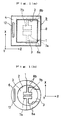
- Figs. 1(a) and (b) are plane views illustrating different embodiments of the ultrathin multimode quartz crystal filter element according to the present invention
- Figs. 2(a) and (b) are a diagram showing the relationship between the crystal axis of a quartz crystal plate and the direction of alignment of split electrodes and a graph showing experimental results about the degree of acoustic coupling obtained by changing the above-mentioned relationship
- Figs. 3(a) and (b) are perspective and sectional views showing the construction of a conventional ultrathin piezoelectric multimode filter.
- Figs. 3(a) and (b) are a perspective view showing the construction of an ultrathin piezoelectric multimode filter studied heretofore and a sectional view showing the state in which the filter element is fixedly mounted in a case.
- the filter element has a cavity 2 formed by mechanical grinding or etching in one side of a block 1 of quartz crystal or similar piezoelectric material substantially centrally thereof so that the bottom of the cavity 2 forms a very thin vibratory portion 3 which is supported by a thick frame-like marginal portion 4 formed integrally therewith.
- a conductive film is evaporated onto the surface of the frame-like marginal portion 4, the inner wall surface of the cavity and the surface of the vibratory portion 3 to form an overall electrode 5 on the side of the piezoelectric block 1 where the caivity 2 is provided. Further, a pair of split electrodes 7a and 7b and electrode lead portions 8a and 8b extending therefrom to and along marginal edges of the block are provided on the flat surface 6 thereof opposite from the overall electrode 5.
- the conventional ultrathin multimode piezoelectric filter element indicated generally by 9, has such a construction.
- the filter element of this type be fixedly mounted upside down--with the cavity 2 facing downward--in a so-called flat type case 10 which is a dish-like molding of an insulator, as shown in Fig. 3(b).
- one portion of the frame-like marginal portion 4 deposited with the overall electrode 5 and a conductive film 11 coated all over the bottom of the case 10 are bonded in only one edge of the marginal portion 4 and fixed to each other by a conductive adhesive 12 and the electrode lead portions 8a and 8b extending from the split electrodes 7a and 7b on the opposite side from the cavity 2 are each connected by a bonding wire 14 to a conductive film13 coated on a stepped portion on the inner wall of the case 10, thereby reducing the restriction of the filter element 9 by the case 10 as much as possible and minimizing distortion which isapplied to the filter element due to the difference in the coefficient of thermal expansion between them.
- the conductive films 11 and 13 on the bottom of the case 10 and on the stepped portions on the inner wall of case 10 are electrically connected to external lead terminals 15 and 16 which hermetically pass through the case 10 and are exposed on the outside thereof.
- Such a piezoelectric device is completed by hermetically sealing the opening of the case 10 with a proper lid 17 (usually made of metal) after the resonator is fixedly mounted in the case 10.
- the degree of acoustic coupling between the split electrodes 7a and 7b appreciably varies according to the direction of their alignment with respect to the crystal axis of the quartz crystal plate used, as in conventional quartz crystal multimode filter elements.
- Figs. 2(a) and (b) shows the relationship between the direction of alignment of the split electrodes with respect to the x-axis of the AT cut quartz crystal plate and the degree of acoustic coupling between the electrodes, i.e. the bandwidth of the filter.
- the bandwidth of the quartz filter element varies about 1.26 times between the z-direction coupling by the alignment of the split electrodes 7a and 7b in the z-axis direction and the x-direction coupling by their alignment in the x-axis direction.
- the conventional multimode piezoelectric filter element usually employs a quartz crystal plate of a fundamental frequency of 30 MHz at the lowest, and of 50 MHz at the highest, however, there is no need of using the structure which provides the acoustic coupling in the x-direction.
- multimode quartz crystal filter elements shown in Figs. 1(a) and (b) each use a quartz crystal plate of about 100MHz fundamental vibration, and in this instance, the manufacture of such filter elements witha satisfactory bandwidth through utilization of the conventional z-direction coupling will encounter with difficulties in the formation of the split electrodes as referred to previously.
- the split electrodes are aligned in x-axis direction, that is, the x-direction coupling which essentially provides a wide bandwidth is utilized.
- the multimode quartz crystal filter element depicted in Fig. 1(a) has a construction in which the substrate is covered with a conductive film on the side where the cavity 2 is provided and the split electrodes 7a and 7b are aligned in the x-axis direction on the opposite side of the ultrathin vibratory portion 3.
- the circular multimode filter element shown in Fig. 1(b) has the split electrodes 7a and 7b aligned in the x-axis direction on the bottom of the cavity 2 and the overall electrode formed all over the substrate on the opposite side therefrom.
- the quartz crystal block 1 may be disc-shaped as shown in Fig. 1(b) and the split electrodes 7a and 7b may also be vapor deposited on flat portion 6 of the block along the x-axis.
- the present invention is remarkably effective in satisfying various characteristics of the multimode quartz crystal filter which employs a quartz crystal substrate of a fundamental frequency above 50 MHz and in improving the yield rate of product.
Landscapes
- Physics & Mathematics (AREA)
- Acoustics & Sound (AREA)
- Chemical & Material Sciences (AREA)
- Crystallography & Structural Chemistry (AREA)
- Piezo-Electric Or Mechanical Vibrators, Or Delay Or Filter Circuits (AREA)
Abstract
Applications Claiming Priority (3)
| Application Number | Priority Date | Filing Date | Title |
|---|---|---|---|
| JP2136135A JPH0435108A (ja) | 1990-05-25 | 1990-05-25 | 超薄板多重モード水晶フィルタ素子 |
| JP136135/90 | 1990-05-25 | ||
| PCT/JP1990/001528 WO1991019352A1 (fr) | 1990-05-25 | 1990-11-22 | Element de filtre en cristal de quartz ultra mince a fonctionnement en mode multiple |
Publications (3)
| Publication Number | Publication Date |
|---|---|
| EP0483358A1 true EP0483358A1 (fr) | 1992-05-06 |
| EP0483358A4 EP0483358A4 (en) | 1992-09-09 |
| EP0483358B1 EP0483358B1 (fr) | 1995-10-11 |
Family
ID=15168127
Family Applications (1)
| Application Number | Title | Priority Date | Filing Date |
|---|---|---|---|
| EP91900352A Revoked EP0483358B1 (fr) | 1990-05-25 | 1990-11-22 | Element de filtre en cristal de quartz ultra mince a fonctionnement en mode multiple |
Country Status (5)
| Country | Link |
|---|---|
| US (1) | US5307034A (fr) |
| EP (1) | EP0483358B1 (fr) |
| JP (1) | JPH0435108A (fr) |
| DE (1) | DE69022996T2 (fr) |
| WO (1) | WO1991019352A1 (fr) |
Families Citing this family (16)
| Publication number | Priority date | Publication date | Assignee | Title |
|---|---|---|---|---|
| US5617065A (en) * | 1995-06-29 | 1997-04-01 | Motorola, Inc. | Filter using enhanced quality factor resonator and method |
| US6081164A (en) * | 1997-01-09 | 2000-06-27 | Seiko Epson Corporation | PLL oscillator package and production method thereof |
| US6298216B1 (en) | 1999-09-21 | 2001-10-02 | Ten Cate Enbi, Inc. | Image transfer device incorporating a fuser roller having a thick wearable silicone rubber surface |
| US7098574B2 (en) * | 2002-11-08 | 2006-08-29 | Toyo Communication Equipment Co., Ltd. | Piezoelectric resonator and method for manufacturing the same |
| WO2009035155A1 (fr) * | 2007-09-13 | 2009-03-19 | Citizen Holdings Co., Ltd. | Pièce d'oscillateur à cristal et son procédé de fabrication |
| WO2011034104A1 (fr) * | 2009-09-18 | 2011-03-24 | 株式会社大真空 | Élément piézoélectrique vibrant et son procédé de fabrication |
| JP5720152B2 (ja) * | 2010-09-06 | 2015-05-20 | 富士通株式会社 | 振動子の作製方法、振動子および発振器 |
| TW201251157A (en) | 2011-06-03 | 2012-12-16 | Seiko Epson Corp | Piezoelectric vibration element, manufacturing method for piezoelectric vibration element, piezoelectric vibrator, electronic device, and electronic apparatus |
| CN102957394B (zh) * | 2011-08-18 | 2016-12-21 | 精工爱普生株式会社 | 振动元件、振子、电子装置、电子设备、移动体及振动元件的制造方法 |
| US8970316B2 (en) | 2011-08-19 | 2015-03-03 | Seiko Epson Corporation | Resonating element, resonator, electronic device, electronic apparatus, and mobile object |
| JP2014007538A (ja) * | 2012-06-25 | 2014-01-16 | Daishinku Corp | 水晶振動デバイス |
| JP6390104B2 (ja) * | 2013-03-05 | 2018-09-19 | セイコーエプソン株式会社 | 振動素子、振動子、発振器、電子機器および移動体 |
| JP6498379B2 (ja) * | 2013-03-29 | 2019-04-10 | セイコーエプソン株式会社 | 振動素子、振動子、発振器、電子機器および移動体 |
| JP6435606B2 (ja) * | 2013-03-29 | 2018-12-12 | セイコーエプソン株式会社 | 振動素子、振動子、発振器、電子機器および移動体 |
| JP6107330B2 (ja) * | 2013-03-29 | 2017-04-05 | セイコーエプソン株式会社 | 振動素子、振動子、発振器、電子機器および移動体 |
| USD760230S1 (en) * | 2014-09-16 | 2016-06-28 | Daishinku Corporation | Piezoelectric vibration device |
Family Cites Families (9)
| Publication number | Priority date | Publication date | Assignee | Title |
|---|---|---|---|---|
| JPS4883752A (fr) * | 1972-02-07 | 1973-11-08 | ||
| FR2279261A1 (fr) * | 1974-07-19 | 1976-02-13 | Thomson Csf | Dispositif electromecanique a resonance et son application au filtrage des signaux de television |
| US3951098A (en) * | 1975-02-12 | 1976-04-20 | Enviro-Gro, Inc. | House plant water content indicator |
| US4218631A (en) * | 1977-06-08 | 1980-08-19 | Kinsekisha Laboratory, Ltd. | Electrode structure for thickness mode piezoelectric vibrating elements |
| JPH03243008A (ja) * | 1990-02-21 | 1991-10-30 | Toyo Commun Equip Co Ltd | 超薄板水晶共振子の固定方法 |
| DE69029086T2 (de) * | 1990-02-09 | 1997-03-06 | Toyo Communication Equip | Struktur zur Festhaltung in einem Modül eines flachen ultradünnen piezoelektrischen Resonators |
| US5075651A (en) * | 1990-02-15 | 1991-12-24 | Motorola, Inc. | VHF wide-bandwidth low impedance monolithic crystal filter having bridged electrodes |
| DE4130632A1 (de) * | 1991-09-14 | 1993-03-18 | Philips Patentverwaltung | Verfahren zum erkennen der gesprochenen woerter in einem sprachsignal |
| JPH05135297A (ja) * | 1991-11-14 | 1993-06-01 | Meidensha Corp | 交通規制情報取得システム |
-
1990
- 1990-05-25 JP JP2136135A patent/JPH0435108A/ja active Pending
- 1990-11-22 DE DE69022996T patent/DE69022996T2/de not_active Revoked
- 1990-11-22 US US07/809,511 patent/US5307034A/en not_active Expired - Fee Related
- 1990-11-22 WO PCT/JP1990/001528 patent/WO1991019352A1/fr not_active Ceased
- 1990-11-22 EP EP91900352A patent/EP0483358B1/fr not_active Revoked
Also Published As
| Publication number | Publication date |
|---|---|
| EP0483358A4 (en) | 1992-09-09 |
| DE69022996T2 (de) | 1996-03-14 |
| WO1991019352A1 (fr) | 1991-12-12 |
| EP0483358B1 (fr) | 1995-10-11 |
| US5307034A (en) | 1994-04-26 |
| JPH0435108A (ja) | 1992-02-05 |
| DE69022996D1 (de) | 1995-11-16 |
Similar Documents
| Publication | Publication Date | Title |
|---|---|---|
| US4365181A (en) | Piezoelectric vibrator with damping electrodes | |
| EP0483358B1 (fr) | Element de filtre en cristal de quartz ultra mince a fonctionnement en mode multiple | |
| EP0484545B1 (fr) | Structure d'electrode et de sortie correspondante pour resonateur piezoelectrique a plaque mince | |
| US6914368B2 (en) | Piezoelectric resonator, and piezoelectric filter, duplexer, and communication apparatus, all including same | |
| JP3229336B2 (ja) | 表面がマイクロ機械加工された音響波ピエゾ電気結晶 | |
| US4418299A (en) | Face-shear mode quartz crystal vibrators and method of manufacture | |
| EP0641073B1 (fr) | Résonateur piézoélectrique encapsulé | |
| JPH0532925B2 (fr) | ||
| US5218328A (en) | Structure for a resonator using an ultrathin piezoelectric substrate | |
| US6741147B2 (en) | Method and apparatus for adjusting the resonant frequency of a thin film resonator | |
| US7888849B2 (en) | Piezoelectric resonator and method for producing the same | |
| JPH11340775A (ja) | 圧電振動子 | |
| JPH0211043B2 (fr) | ||
| JP4196641B2 (ja) | 超薄板圧電デバイスとその製造方法 | |
| US6016025A (en) | Selected overtone resonator with channels | |
| JP2001257560A (ja) | 超薄板圧電振動素子の電極構造 | |
| JP3277501B2 (ja) | 圧電共振子の構造及びその製造方法 | |
| JPS58137318A (ja) | 薄膜圧電振動子 | |
| JP4513150B2 (ja) | 高周波圧電振動子 | |
| KR940009397B1 (ko) | 초박판 다중모드 수정필터소자 | |
| JP2007189492A (ja) | 圧電基板の製造方法、圧電基板、圧電振動子、及び圧電発振器 | |
| JP2002368573A (ja) | 超薄板圧電振動子及びその製造方法 | |
| JPH03243008A (ja) | 超薄板水晶共振子の固定方法 | |
| JP3102872B2 (ja) | 超薄肉圧電振動子 | |
| JP2001060844A (ja) | 複合圧電振動子 |
Legal Events
| Date | Code | Title | Description |
|---|---|---|---|
| PUAI | Public reference made under article 153(3) epc to a published international application that has entered the european phase |
Free format text: ORIGINAL CODE: 0009012 |
|
| 17P | Request for examination filed |
Effective date: 19920220 |
|
| AK | Designated contracting states |
Kind code of ref document: A1 Designated state(s): DE FR GB |
|
| A4 | Supplementary search report drawn up and despatched |
Effective date: 19920721 |
|
| AK | Designated contracting states |
Kind code of ref document: A4 Designated state(s): DE FR GB |
|
| 17Q | First examination report despatched |
Effective date: 19950209 |
|
| GRAA | (expected) grant |
Free format text: ORIGINAL CODE: 0009210 |
|
| AK | Designated contracting states |
Kind code of ref document: B1 Designated state(s): DE FR GB |
|
| REF | Corresponds to: |
Ref document number: 69022996 Country of ref document: DE Date of ref document: 19951116 |
|
| ET | Fr: translation filed | ||
| PLAV | Examination of admissibility of opposition |
Free format text: ORIGINAL CODE: EPIDOS OPEX |
|
| PLBQ | Unpublished change to opponent data |
Free format text: ORIGINAL CODE: EPIDOS OPPO |
|
| PLBI | Opposition filed |
Free format text: ORIGINAL CODE: 0009260 |
|
| 26 | Opposition filed |
Opponent name: COMPOSANTS QUARTZ ET ELECTRONIQUE Effective date: 19960610 |
|
| PLAV | Examination of admissibility of opposition |
Free format text: ORIGINAL CODE: EPIDOS OPEX |
|
| PLBF | Reply of patent proprietor to notice(s) of opposition |
Free format text: ORIGINAL CODE: EPIDOS OBSO |
|
| PGFP | Annual fee paid to national office [announced via postgrant information from national office to epo] |
Ref country code: FR Payment date: 19961111 Year of fee payment: 7 |
|
| PGFP | Annual fee paid to national office [announced via postgrant information from national office to epo] |
Ref country code: GB Payment date: 19961113 Year of fee payment: 7 |
|
| PGFP | Annual fee paid to national office [announced via postgrant information from national office to epo] |
Ref country code: DE Payment date: 19961202 Year of fee payment: 7 |
|
| PLBF | Reply of patent proprietor to notice(s) of opposition |
Free format text: ORIGINAL CODE: EPIDOS OBSO |
|
| RDAH | Patent revoked |
Free format text: ORIGINAL CODE: EPIDOS REVO |
|
| RDAG | Patent revoked |
Free format text: ORIGINAL CODE: 0009271 |
|
| STAA | Information on the status of an ep patent application or granted ep patent |
Free format text: STATUS: PATENT REVOKED |
|
| GBPR | Gb: patent revoked under art. 102 of the ep convention designating the uk as contracting state |
Free format text: 970125 |
|
| 27W | Patent revoked |
Effective date: 19970125 |