EP0483513A2 - Circuit pour réduction du dépassement - Google Patents
Circuit pour réduction du dépassement Download PDFInfo
- Publication number
- EP0483513A2 EP0483513A2 EP91116402A EP91116402A EP0483513A2 EP 0483513 A2 EP0483513 A2 EP 0483513A2 EP 91116402 A EP91116402 A EP 91116402A EP 91116402 A EP91116402 A EP 91116402A EP 0483513 A2 EP0483513 A2 EP 0483513A2
- Authority
- EP
- European Patent Office
- Prior art keywords
- circuit
- output
- coupled
- input
- terminal
- Prior art date
- Legal status (The legal status is an assumption and is not a legal conclusion. Google has not performed a legal analysis and makes no representation as to the accuracy of the status listed.)
- Withdrawn
Links
Images

Classifications
-
- H—ELECTRICITY
- H03—ELECTRONIC CIRCUITRY
- H03K—PULSE TECHNIQUE
- H03K17/00—Electronic switching or gating, i.e. not by contact-making and –breaking
- H03K17/16—Modifications for eliminating interference voltages or currents
- H03K17/161—Modifications for eliminating interference voltages or currents in field-effect transistor switches
- H03K17/165—Modifications for eliminating interference voltages or currents in field-effect transistor switches by feedback from the output circuit to the control circuit
- H03K17/166—Soft switching
Definitions
- the present invention relates to a circuit for reducing output and ground voltage undershoot on the ground reference of the circuit, preferably a CMOS circuit.
- Transient noise can be a problem in CMOS circuits having multiple switching outputs.
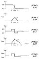
- V OUT When the output of a CMOS circuit makes a transition from a logic high state to a logic low state as illustrated by signal V OUT in FIG. 1A, any load capacitance at the output of the CMOS circuit will typically discharge through a package parasitic inductance thereby providing a current to ground as illustrated by signal I GND in FIG. 1B.
- the signal I GND is the derivative of signal V OUT where it is assumed that the capacitor of interest is the load capacitor
- time T MAX shown in FIG.
- the positive portion of signal V GND represents the overshoot voltage or the positive ground bounce
- the negative portion of signal V GND represents the undershoot voltage or the negative ground bounce wherein both positive and negative ground bounce occur as a result of the output of the CMOS circuit making a transition from a logic high state to a logic low state.
- the slope of line segment 12 in FIG. 1B could be decreased as shown by line segment 14 in FIG. 1D
- the time duration of the undershoot voltage would be increased, but the peak negative voltage of the undershoot voltage would be substantially reduced as illustrated by signal V GND in FIG. 1E.
- the peak negative undershoot voltage is typically of greater importance than the duration of the voltage undershoot since large negative undershoot voltages can create dynamic threshold problems as is known.
- the present invention provides a circuit for reducing negative ground bounce having an input signal applied at an input terminal thereof and an output signal supplied at an output terminal thereof, comprising; an output buffer having an input and an output, said input being responsive to the input signal, and said output being coupled to the output terminal of the circuit for providing the output signal; gate means having first and second inputs responsive to the input signal and the output signal for providing a control signal at an output thereof, said control signal being in a first logic state when the input signal and the output signal are in predetermined logic states; and injector means responsive to said control signal and to the input signal for providing a predetermined current to the output terminal of the circuit wherein said injector current decreases the negative peak undershoot voltage occurring in a ground reference of the circuit.
- a circuit for reducing negative ground bounce having an input terminal and an output terminal comprising an output buffer having an input and an output, the input being coupled to the input terminal of the circuit, and the output being coupled to the output terminal of the circuit; a gate circuit having first and second inputs and an output, the first input being coupled to the input terminal of the circuit, and the second input being coupled to the output terminal of the circuit; an injector circuit for providing a predetermined current to the output terminal of the circuit, the injector circuit includes a first transistor having first, second and control electrodes, the second electrode being coupled to a first supply voltage terminal, and the control electrode being coupled to the output of the gate circuit; and a second transistor having first, second and control electrodes, the first electrode being coupled to the first electrode of the first transistor, the second electrode being coupled to the output terminal of the circuit, and the control electrode being coupled to the input terminal of the circuit.
- FIGS. 1A-1E are graphical waveforms illustrating various voltage and current signals when the output of a CMOS circuit makes a transition from a logic high state to a logic low state.
- FIG. 2 is a partial schematic diagram of a CMOS circuit having reduced output and ground voltage undershoot in accordance with the present invention.
- FIG. 3 is a partial schematic diagram of an alternate CMOS circuit having reduced output and ground voltage undershoot in accordance with the present invention.
- CMOS circuit 20 having reduced output and ground voltage undershoot is shown comprising output buffer 22 having an input coupled to terminal 24 at which the voltage V IN is applied.
- the output of output buffer 22 is coupled to terminal 26 for providing voltage V OUT .
- NOR gate 28 has a first input coupled to terminal 24 and a second input coupled to terminal 26.
- Inverter 30 has an input coupled to terminal 24 and an output coupled to the gate electrode of N-channel MOS transistor 32.
- the source electrode of N-channel MOS transistor 32 is coupled to terminal 26 while the drain electrode of the same is coupled to the drain electrode of P-channel MOS transistor 34.
- the source of P-channel MOS transistor 34 is coupled to a first supply voltage terminal at which the operating potential V CC is applied.
- Resistor 36 is coupled between an output of NOR gate 28 and the gate electrode of P-channel MOS transistor 34.
- NOR gate 28 includes P-channel MOS transistor 38 which has its source electrode coupled to operating potential V CC and its drain electrode coupled to the source electrode of P-channel MOS transistor 40.
- the drain electrode of P-channel MOS transistor 40 is coupled to the output of NOR gate 28 and to the drain electrodes of N-channel MOS transistors 42 and 44.
- the gate electrodes of P-channel MOS transistor 40 and N-channel MOS transistor 42 are coupled to the first input of NOR gate 28.
- the gate electrodes of P-channel MOS transistor 38 and N-channel MOS transistor 44 are coupled to the second input of NOR gate 28.
- the source electrodes of N-channel MOS transistors 42 and 44 are returned to ground potential.
- NOR gate 28 functions in a well known manner such that if a logic low appears at both of its first and second inputs, the output of NOR gate 28 will be a logic high. Further, if a logic high is present at either the first input or second input, or both inputs of NOR gate 28, the output of NOR gate 28 provides a logic low. Assuming an initial starting point where voltage V IN is indicative of a logic high voltage level, voltage V OUT provided at terminal 26 is also a logic high voltage level via non-inverting output buffer 22. The logic high voltage level appearing at terminal 24 provides a logic low voltage level at the gate electrode of transistor 32 via inverter 30, thereby rendering transistor 32 non-operative.
- the logic high voltage levels present at terminals 24 and 26 respectively provide logic high voltage levels at the first and second inputs of NOR gate 28. Accordingly, NOR gate 28 responds to provides a logic low voltage level at its output which is transferred to the gate electrode of transistor 34 via resistor 36.
- P-channel MOS transistor 34 will not be conduct current since N-channel MOS transistor 32 is non-operative as aforementioned.
- N-channel MOS transistor 32 as well as P-channel MOS transistor 34 conduct substantially zero current and, thus, inject substantially zero current to terminal 26.
- the voltage level provided at terminal 26 begins to transition from a logic high voltage level to a logic low voltage level via non-inverting output buffer 22.
- the logic low voltage level occurring at terminal 24 is immediately transferred to the gate electrode of N-channel MOS transistor 32 via inverter 30. Note however that N-channel MOS transistor 32 will not be rendered operative yet since the voltage at terminal 26 is still substantially equal to a logic high voltage level.
- N-channel MOS transistor 32 will be rendered operative.
- P-channel MOS transistor 34 will conduct current since its gate electrode is at a logic low and N-channel MOS transistor 32 is operative.
- N-channel MOS transistor 32 and P-channel MOS transistor 34 when operative, function as an injector circuit to inject a feedthrough current to terminal 26.
- the feedthrough current injected to terminal 26 will add in with the current signal I GND which will result in decreasing the slope of the ground current signal (I GND ) as aforedescribed and illustrated by segment 14 in FIG. 1D.
- V MIN negative peak undershoot voltage
- This feedthrough current will continue to be injected into terminal 26 until the voltage at the gate electrode of P-channel MOS transistor 34 has increased to a predetermined threshold voltage such that P-channel MOS transistor 34 is rendered non-operative. Further, P-channel MOS transistor will be rendered non-operative when the voltage at terminal 26 falls to a predetermined voltage threshold such that the output of NOR gate 28 switches from its original logic low voltage level to a logic high voltage level and when the logic high voltage level occurring at the output of NOR gate 28 is transferred to the gate electrode of P-channel MOS transistor 34 via an RC time constant delay as determined by resistor 36 and an internal gate electrode capacitance associated with P-channel MOS transistor 34. If P-channel MOS transistor 34 is rendered non-operative, substantially zero current will be injected into terminal 26 since N-channel MOS transistor 32 will not be able to pull current out of operating potential VCC.
- resistor 36 can be implemented by a transistor having its first and second electrodes coupled between the output of NOR gate 28 and the gate electrode of P-channel MOS transistor 34, while its control electrode is biased to a predetermined reference voltage.
- NOR gate 28 is not intended to be restricted to just a NOR function. but can be a plurality of gating circuits for example, an AND, OR or NAND gate.
- FIG. 3 a partial schematic diagram of an alternate CMOS circuit having reduced output and voltage undershoot is shown. It is understood that components similar to those of FIG. 2 are designated by the same reference numerals.
- the circuit in FIG. 3 includes additional tri-state circuitry over the circuit in FIG. 2.
- the tri-state circuitry comprises P-channel MOS transistor 46 and N-channel MOS transistor 50.
- output buffer 22 has been replaced by output buffer 54 which includes two additional differential enable inputs (EN and EN ⁇ ).
- the circuit of FIG. 3 further includes P-channel MOS transistor 46 having a source coupled to operating potential V CC and a gate electrode coupled to terminal 48 at which enable signal EN is applied.
- the drain electrode of P-channel MOS transistor 46 is coupled to the source electrode of P-channel MOS transistor 38 of NOR gate 28.
- N-channel MOS transistor 50 has a drain electrode coupled to the source electrode of N-channel MOS transistor 32 and a source electrode coupled to terminal 26.
- the gate electrode of N-channel MOS transistor 50 is coupled to terminal 52 at which an inverted enable signal EN ⁇ is applied.
- output buffer 54 has an input and an output which functions identical to output buffer 22.
- output buffer 54 has EN and EN ⁇ inputs which are respectively coupled to terminals 48 and 52 for tri-state operation.
- the operation of the circuit in FIG. 3 is identical to the aforedescribed operation of the circuit in FIG. 2 when signals EN and EN ⁇ are respectively at a logic low and logic high state wherein P-channel MOS transistor 46 as well as N-channel MOS transistor 50 are operative. Further, output buffer 22 is enabled. However, when signal EN is at a logic high state and signal EN ⁇ is at a logic low state, P-channel MOS transistor 46 and N-channel MOS transistor 50 are rendered non-operative thereby indicative of a tri-state condition. Further, output buffer 22 will be disabled thereby providing a high impedance at its respective input and output. Since N-channel MOS transistor 50 is rendered non-operative, substantially zero feedthrough current will be injected at terminal 26.
Landscapes
- Logic Circuits (AREA)
- Electronic Switches (AREA)
Applications Claiming Priority (2)
| Application Number | Priority Date | Filing Date | Title |
|---|---|---|---|
| US605203 | 1990-10-29 | ||
| US07/605,203 US5055714A (en) | 1990-10-29 | 1990-10-29 | Undershoot reduction circuit |
Publications (2)
| Publication Number | Publication Date |
|---|---|
| EP0483513A2 true EP0483513A2 (fr) | 1992-05-06 |
| EP0483513A3 EP0483513A3 (en) | 1992-07-29 |
Family
ID=24422660
Family Applications (1)
| Application Number | Title | Priority Date | Filing Date |
|---|---|---|---|
| EP19910116402 Withdrawn EP0483513A3 (en) | 1990-10-29 | 1991-09-26 | Undershoot reduction circuit |
Country Status (3)
| Country | Link |
|---|---|
| US (1) | US5055714A (fr) |
| EP (1) | EP0483513A3 (fr) |
| JP (1) | JPH05175798A (fr) |
Cited By (1)
| Publication number | Priority date | Publication date | Assignee | Title |
|---|---|---|---|---|
| EP0486880B1 (fr) * | 1990-11-19 | 1996-07-31 | National Semiconductor Corporation | Circuit à grande vitesse anti-suroscillations et sousoscillations |
Families Citing this family (5)
| Publication number | Priority date | Publication date | Assignee | Title |
|---|---|---|---|---|
| US5604453A (en) * | 1993-04-23 | 1997-02-18 | Altera Corporation | Circuit for reducing ground bounce |
| US5410189A (en) * | 1993-09-27 | 1995-04-25 | Xilinx, Inc. | Input buffer having an accelerated signal transition |
| US5428303A (en) * | 1994-05-20 | 1995-06-27 | National Semiconductor Corporation | Bias generator for low ground bounce output driver |
| US5734277A (en) * | 1996-02-05 | 1998-03-31 | Motorola, Inc. | Output circuit and method for suppressing switching noise therein |
| US6359478B1 (en) | 2001-08-31 | 2002-03-19 | Pericom Semiconductor Corp. | Reduced-undershoot CMOS output buffer with delayed VOL-driver transistor |
Family Cites Families (5)
| Publication number | Priority date | Publication date | Assignee | Title |
|---|---|---|---|---|
| US4498021A (en) * | 1982-07-13 | 1985-02-05 | Matsushita Electric Industrial Co., Ltd. | Booster for transmitting digital signal |
| US4970419A (en) * | 1987-03-23 | 1990-11-13 | Unisys Corporation | Low-noise transmission line termination circuitry |
| US4890015A (en) * | 1988-01-29 | 1989-12-26 | Texas Instruments Incorporated | Method and circuitry for controlling the compensation of negative internal ground voltage fluctuations |
| EP0369055A1 (fr) * | 1988-11-17 | 1990-05-23 | Siemens Aktiengesellschaft | Circuit de compensation des signaux de bruit |
| US4959561A (en) * | 1989-01-04 | 1990-09-25 | Motorola, Inc. | MOS output buffer with reduced supply line disturbance |
-
1990
- 1990-10-29 US US07/605,203 patent/US5055714A/en not_active Expired - Fee Related
-
1991
- 1991-09-26 EP EP19910116402 patent/EP0483513A3/en not_active Withdrawn
- 1991-10-23 JP JP3302717A patent/JPH05175798A/ja active Pending
Cited By (1)
| Publication number | Priority date | Publication date | Assignee | Title |
|---|---|---|---|---|
| EP0486880B1 (fr) * | 1990-11-19 | 1996-07-31 | National Semiconductor Corporation | Circuit à grande vitesse anti-suroscillations et sousoscillations |
Also Published As
| Publication number | Publication date |
|---|---|
| EP0483513A3 (en) | 1992-07-29 |
| US5055714A (en) | 1991-10-08 |
| JPH05175798A (ja) | 1993-07-13 |
Similar Documents
| Publication | Publication Date | Title |
|---|---|---|
| US4970408A (en) | CMOS power-on reset circuit | |
| US4779013A (en) | Slew-rate limited output driver having reduced switching noise | |
| US4877978A (en) | Output buffer tri-state noise reduction circuit | |
| JP2996301B2 (ja) | 負荷及び時間適応電流供給ドライブ回路 | |
| US5128560A (en) | Boosted supply output driver circuit for driving an all N-channel output stage | |
| US5633600A (en) | Output buffer circuit having a minimized output voltage propagation | |
| JP2922028B2 (ja) | 半導体集積回路の出力回路 | |
| US5748019A (en) | Output buffer driver with load compensation | |
| US5367210A (en) | Output buffer with reduced noise | |
| US4628218A (en) | Driving circuit suppressing peak value of charging current from power supply to capacitive load | |
| US4902914A (en) | Logic circuit used in standard IC or CMOS logic level | |
| KR950000525B1 (ko) | 캐패시턴스 디바이스 구동용 cmos 집적 회로 | |
| US5877635A (en) | Full-swing buffer circuit with charge pump | |
| KR940005509B1 (ko) | 승압단속회로및이를구비하는출력버퍼회로 | |
| US5233238A (en) | High power buffer with increased current stability | |
| US4453121A (en) | Reference voltage generator | |
| US4642488A (en) | CMOS input buffer accepting TTL level inputs | |
| JPH04229714A (ja) | バッファを有する集積回路 | |
| US6236195B1 (en) | Voltage variation correction circuit | |
| US5055714A (en) | Undershoot reduction circuit | |
| JPH01149448A (ja) | 集積ディジタル回路 | |
| EP0035345A1 (fr) | Circuit de remise activé lors de la mise sous tension | |
| US4352996A (en) | IGFET Clock generator circuit employing MOS boatstrap capacitive drive | |
| US5038058A (en) | BiCMOS TTL output driver | |
| KR20040062646A (ko) | 향상된 제어 회로를 포함하는 출력 드라이버 |
Legal Events
| Date | Code | Title | Description |
|---|---|---|---|
| PUAI | Public reference made under article 153(3) epc to a published international application that has entered the european phase |
Free format text: ORIGINAL CODE: 0009012 |
|
| AK | Designated contracting states |
Kind code of ref document: A2 Designated state(s): DE FR GB |
|
| PUAL | Search report despatched |
Free format text: ORIGINAL CODE: 0009013 |
|
| AK | Designated contracting states |
Kind code of ref document: A3 Designated state(s): DE FR GB |
|
| 17P | Request for examination filed |
Effective date: 19930114 |
|
| STAA | Information on the status of an ep patent application or granted ep patent |
Free format text: STATUS: THE APPLICATION IS DEEMED TO BE WITHDRAWN |
|
| 18D | Application deemed to be withdrawn |
Effective date: 19950401 |