EP0483669A2 - Verfahren zur Herstellung einer dünnen Schicht und Halbleitervorrichtungen - Google Patents
Verfahren zur Herstellung einer dünnen Schicht und Halbleitervorrichtungen Download PDFInfo
- Publication number
- EP0483669A2 EP0483669A2 EP91118166A EP91118166A EP0483669A2 EP 0483669 A2 EP0483669 A2 EP 0483669A2 EP 91118166 A EP91118166 A EP 91118166A EP 91118166 A EP91118166 A EP 91118166A EP 0483669 A2 EP0483669 A2 EP 0483669A2
- Authority
- EP
- European Patent Office
- Prior art keywords
- contact hole
- plasma
- gas
- introducing
- nitride film
- Prior art date
- Legal status (The legal status is an assumption and is not a legal conclusion. Google has not performed a legal analysis and makes no representation as to the accuracy of the status listed.)
- Granted
Links
Images







Classifications
-
- H—ELECTRICITY
- H10—SEMICONDUCTOR DEVICES; ELECTRIC SOLID-STATE DEVICES NOT OTHERWISE PROVIDED FOR
- H10W—GENERIC PACKAGES, INTERCONNECTIONS, CONNECTORS OR OTHER CONSTRUCTIONAL DETAILS OF DEVICES COVERED BY CLASS H10
- H10W20/00—Interconnections in chips, wafers or substrates
- H10W20/01—Manufacture or treatment
- H10W20/031—Manufacture or treatment of conductive parts of the interconnections
- H10W20/032—Manufacture or treatment of conductive parts of the interconnections of conductive barrier, adhesion or liner layers
- H10W20/033—Manufacture or treatment of conductive parts of the interconnections of conductive barrier, adhesion or liner layers in openings in dielectrics
-
- H—ELECTRICITY
- H10—SEMICONDUCTOR DEVICES; ELECTRIC SOLID-STATE DEVICES NOT OTHERWISE PROVIDED FOR
- H10P—GENERIC PROCESSES OR APPARATUS FOR THE MANUFACTURE OR TREATMENT OF DEVICES COVERED BY CLASS H10
- H10P14/00—Formation of materials, e.g. in the shape of layers or pillars
- H10P14/40—Formation of materials, e.g. in the shape of layers or pillars of conductive or resistive materials
- H10P14/42—Formation of materials, e.g. in the shape of layers or pillars of conductive or resistive materials using a gas or vapour
- H10P14/43—Chemical deposition, e.g. chemical vapour deposition [CVD]
-
- Y—GENERAL TAGGING OF NEW TECHNOLOGICAL DEVELOPMENTS; GENERAL TAGGING OF CROSS-SECTIONAL TECHNOLOGIES SPANNING OVER SEVERAL SECTIONS OF THE IPC; TECHNICAL SUBJECTS COVERED BY FORMER USPC CROSS-REFERENCE ART COLLECTIONS [XRACs] AND DIGESTS
- Y10—TECHNICAL SUBJECTS COVERED BY FORMER USPC
- Y10S—TECHNICAL SUBJECTS COVERED BY FORMER USPC CROSS-REFERENCE ART COLLECTIONS [XRACs] AND DIGESTS
- Y10S438/00—Semiconductor device manufacturing: process
- Y10S438/909—Controlled atmosphere
Definitions
- the present invention relates to a method for forming a thin film and semiconductor device and more particularly to a method for forming a thin film, such as TiN film formed as a barrier layer on the inside surface of a contact hole in a Semiconductor device and to the semiconductor device in which said thin film was formed.
- a thin film such as TiN film formed as a barrier layer on the inside surface of a contact hole in a Semiconductor device and to the semiconductor device in which said thin film was formed.
- a contact section in a semiconductor device such as LSI has a diffusion layer on the surface of a substrate as a base, connected with an interconnection such as Al through a contact hole.
- Al alloys e. g. Al-1%Si
- Al-1%Si previously contaminated with about 0.5-2% of Si are used as electrode connection material, but even these Al alloys are recently insufficient to prevent deposition of Si as a diameter of a contact hole is smaller than before.
- a TiN film is known as a barrier metal on account of its small electrical resistance and chemical stability (Yamanishi, Yoshihara, Kitahara, and Hosokawa; "Vacuum”, Vol.30 No.5 P347, 1987).
- a TiN film was so far formed by Reactive Sputtering method.
- the Reactive Sputtering method is how to form a TiN film on a substrate 31 by using Ti as a target 30 and providing Ar and N2 as sputtering gas in such an device as shown in Fig.21 (Kanamori; "Vacuum”, Vol.29 No .9 P418, 1986).
- Reference numeral 32 designates a coil.
- LPCVD method Low Pressure Chemical Vapor Deposition method
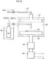
- a method for forming a thin film having good Step Coverage This method is how to form a TiN film on a substrate by thermal reaction with using TiCl4, and NH3 or N2 gas as materials in such an device as shown in Fig.23 (N.Yokoyama et al., Vol.136 No.3, J.Electrochem.Soc., P882)(N.Yokoyama et al.,Vol.138 No.1, J.Electrochem.Soc., P190).
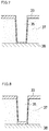
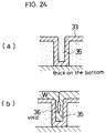
- a TiN film 33 is sufficiently formed on the bottom of a contact hole 35, which is preferable as a barrier metal; however, simultaneously a TiN film of the same thickness as that on the bottom of the contact hole 35 is formed on the side wall of the contact hole.
- the formation of a thick film of TiN on the side wall like this results in a small diameter of a hole remained in the contact hole 35; substantially it is the same situation in which a contact hole of big aspect ratio is formed. Consequently, in the next step, when W(tungsten) or Al and the like filled in, a void 36 occurs in the contact hole 35 as shown in Fig.24(b); it is another problem so as to maintain reliability of a LSI device.
- Reference numeral 40 designates a chamber, wherein a gas nozzle 41 and a sample stage 42 are arranged, and on the sample stage 42, a substrate 43 is placed.
- the bottom of the chamber 40 is connected with a booster pump 44 and a rotary pump 45, and the gas nozzle 41 is connected with a pipe 47 for NH3 gas supply.
- the present invention chiefly consists of using Ar, H2, N2 gas and a metallic compound gas, generating a plasma in a plasma generation chamber by action of electric field generated by a microwave and a magnetic field generated by an exciting coil arranged around, and introducing the generated plasma into a reaction chamber, resulting in forming a thin film of metal nitride on a sample placed on a sample stage.
- a method for forming a thin film according to the present invention has characteristics as follows;
- Ar and H2 gas are supplied in a plasma generation chamber so as to accelerate the film forming, while a metallic compound gas such as TiCl4 is introduced into a reaction chamber, and with passing through an exciting coil supplied derect current, a microwave is introduced in the plasma generation chamber through a wave guide and a microwave inlet window.
- the microwave introduced in the plasma generation chamber activates Ar, H2 and N2 gas supplied in the plasma generation chamber, resulting in generating a plasma.
- said metallic compound gas reacts on said plasma, resulting in providing metal nitride on the surface of a sample placed in the reaction chamber and forming a metal nitride film thereon.
- a metal nitrite film is formed on the surface of the sample.
- Ar is introduced in order to stabilize plasma discharge, and when RF is applied to the microwave inlet window in order to prevent a conductivity film from depositing on said window, Ar also acts as a sputtering gas of the conductivity film.
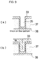
- the generated plasma is supplied to the sample with good directivity, so that a metal nitride film is formed in the contact hole 35 as shown in Fig.9(a). Consequently, in the next step, when interconnction material such as W or Al is plugged up in the contact hole 35, no voids occur and plugging up is carried out as shown in Fig.9(b), resulting in achievement of flattening interconnction.
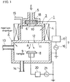
- the plasma CVD apparatus comprises a main body 3 comprising a plasma generation chamber 1 and a reaction chamber 2, an exciting coil 4 arranged around the plasma generation chamber 1 and connected with a direct current power source (not shown), a wave guide 5 introducing a microwave generated from a microwave generator (not shown) into the plasma generation chamber 1, and so on.
- Reference numeral 6 designates a microwave inlet window comprising a quarty glass etc.
- reference numeral 7 designates a radio frequency generator to apply to a radio frequency (RF) power supply on the microwave inlet window
- reference numeral 8 designates a sample stage on which a sample 9 is placed.
- RF radio frequency
- the plasma generation chamber 1 formed in mostly cylindrical shape with the first opening 10 for introducing a microwave formed almost at a center of the upper wall thereof , and below the plasma generation chamber 1, a reaction chamber 2 having larger diameter than the plasma generation chamber 1, are formed in one body.
- the reaction chamber 2 and the plasma generation chamber are devided by a diaphragm 11 with the second opening (for plasma extraction) 12 formed almost at a center thereof.
- the first guide pipe 13 is connected, at the bottom of the reaction chamber 2 an exhaust pipe 14 connected with exhaust system (not shown) is connected.
- the second guide pipe 15 is connected.
- High frequency generation source 7 comprises a high frequency oscillator 16 and a matching box 17, a flat electrode 18 inserted between the microwave inlet window 6 and the wave guide 5, RF is applied to the microwave inlet window 6.
- the sample stage 8 is connected with a RF radio frequency oscillator 21 for applying RF radio frequency to the sample 9 through a matching box 20. Applying the prescribed radio frequency to the sample 9 by the radio frequency oscillator 21, and operating the above-mentioned method for forming a thin film, makes it possible to form a thin film having good Step Coverage even in case of high aspect ratio.
- B magnetic flux density (T)
- angle frequency ⁇ of a microwave was established at 2.45 GHz, and by said formula 1 magnetic flux density B to fulfill the ECR condition was established at 8.75 ⁇ 10 ⁇ 2 T.
- the pressure in the main body 3 was reduced to less than 1 ⁇ 10 ⁇ 6 Torr, after that, while TiCl4 is supplied at a flow rate of 5 ⁇ 15 SCCM into the reaction chamber 2 through the first guide pipe 13, Ar at a flow rate of 43 SCCM, N2 at a flow rate of 15 SCCM, and H2 at a flow rate of 50 SCCM, were supplied into the plasma generation chamber 1 through the second guide pipe 15. After that, the pressure in the main body 3 was established in the prescribed pressure, such as 2 ⁇ 10 ⁇ 3 Torr.
- the plasma passed through the second opening 12, introduced into the reaction chamber 2 with acceleration by the divergent magnetic field to the direction of an arrow A in Fig.1, and formed a thin film of TiN on the surface of the sample 9 having a hole with aspect ratio of 0.2 ⁇ 1.0 placed on the sample stage 8.
- Fig. 2 is a diagrammatic sectional view showing another plasma CVD apparatus used for the method of forming a thin film according to the present invention.
- the plasma gas formed by the action of the electric field generated the microwave introduced through the wave guide 5 into the plasma generation chamber 1 and the magnetic field generated by the exciting coil 4, is introduced into the reaction chamber 2 by the divergent magnetic field generated by the exciting coil 4. And the plasma gas is provided on the surface of the sample 9, on which a TiN film is formed.
- flow rate of Ar gas was 43 SCCM, that of N2 gas was 15 SCCM, that of H2 gas was 50 SCCM, and that of TiCl4 gas was 10 SCCM; and temperature of the sample 9 was 600°C.
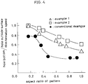
- Fig. 4 contrasted the examples 1,2 and the result of the experiment disclosed in Japanese Patent Laid-Open Publication No.3072/90 as a prior art, the relationship between aspect ratio and hole bottom / hole outside surface film forming speed is shown. It is obvious from Fig. 4 that at high aspect ratio, hole bottom / hole outside surface film forming speed is excellent.
- an insulating film of SiO2 was formed on a P-type Si substrate, wherein a contact hole was formed; by using the apparatus shown in Fig. 1 with the substrate as a sample, a thin film of TiN was formed on the inside surface of the contact hole.
- FIG. 5 A diagram based on the photomicrograph of the SEM scanning electron microscope, wherein a TiN film actually deposisited on the inside surface of the contact hole of aspect ratio 2, is show in Fig. 5.
- the deposition conditions were gas pressure 1.3 mTorr, microwave power 2.8kw, substrate temperature 550°C, TiCl4: 10 SCCM, H2: 50 SCCM, N2: 15 SCCM, and Ar: 43 SCCM.
- a TiN film 33 deposisited on the side wall and bottom of the contact hole 35 The film thickness on the bottom was about 500 ⁇ 600 ⁇ , and that on the side wall was 200 ⁇ 300 ⁇ , while that on the insulating film was 1000 ⁇ . In other words, the thickness of film forming on the bottom of the contact hole 35 could be over 50 % of that on the substrate surface.
- the diagram based on the photomicrograph of SEM in Fig. 8, shows the state of film formation under such conditions as pressure 0.7 mTorr, TiCl4: 5 SCCM, Ar:H2: 50 SCCM, N2: 15 SCCM, microwave power 2.8kw, and substrate temperature 550 °C. It is obvious from this diagram that the thickness of film forming on the bottom of the contact hole 35 was 70 % of that on the substrate surface, very excellent percentage.
- pressure in the main body 3 is set up at 2.0 mTorr, preferably less than 1.3 mTorr.
- the plasma CVD method comprises activating gas by turning it into a plasma, introducing the activated gas along divergent magnetic flux line onto the sample, and forming a TiN film thereon. Accordingly, the activated gas molecules have orientation because of induced by the divergent magnetic field, and are irradiated on the sample almost vertically, resulting in that the TiN film on the surface of the insulation arround the contact hole and on the bottom of that gets thick, while the TiN film on the side wall of the contact hole gets thin.
- the TiN film is thick on the bottom of the contact hole, it has good barrier characteristic, while since the TiN film is thin on the side wall of the contact hole, the diameter of the contact hole doesn't get so small, resulting in not so high aspect ratio after the TiN film forming. As a result, in the next step, wherein electrode materials Al and W(tungsten) are filled in, probability of forming voids decreases, resulting in that highly reliable interconnection is possible.
- Fig. 9(a) the state of the TiN film 33 deposition arround the contact hole 35 by the plasma CVD method according to the present invention is shown, and later, the state after filling in with W(tungsten) is shown in Fig. 9(b).
- Table 1 data of the film thickness formed by each film formation is shown.
- a film formed on the bottom is thick, and in addition, in the next step of filling in with tungsten no voids occurs.
- a curve written with ( ⁇ ) in Fig. 10 indicates the relationship between the film resistivity of a thin film formed at microwave power 1kw, gas pressure 1.3 mTorr in the above-mentioned CVD apparatus and temperature of the substrate. That is, at the substrate temperature of more than 450°C, the film resistivity of a formed TiN film in comparison with 523 ⁇ ⁇ cm, the value obtained by the LPCVD method described in a prior art, became less than 200 ⁇ ⁇ cm, very small value, which is very excellent value in view of the function of electrically connecting the diffusion layer part and the electrode part of metal interconnection in the semiconductor device. On the contrary, when the substrate temperature is less than 450°C, the film resistivityvalue of the formed TiN film abruptly increases, resulting in making the TiN film unsuitable for use.
- a curve written with ⁇ in the Fig. 10 indicates the relationship between the forming speed of a TiN film and the substrate temperature under the conditions of microwave power 1kw and gas pressure 1.3 mTorr.
- the curve says that there is no special correlation between both of them. Consequently, it is better to keep the temperature of the substrate at more than 450°C, preferably 550°C.
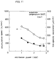
- Fig. 11 indicates the relationship between microwave power and film forming speed ( ⁇ ) and that between microwave power and film resistivity ( ⁇ ). It was comfirmed from Fig. 11 that the specific resistance of less than 200 ⁇ ⁇ cm at the microwave power of more than 1kw, and less than 100 ⁇ ⁇ cm at more than 2kw are obtained.
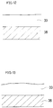
- the deposition conditions are microwave power 1kw and the same as the deposition conditions shown in Fig. 5, except changing the flow rate of TiCl4 gas. It was comfirmed from this Fig. 12 that the deposited TiN film doesn't have calum structure but homogenous fine structure. Accordingly, it was expected that it has a good barrier characteristic.
- Figs. 13, 14,and 15 The cases of TiCl4: 5 SCCM, TiCl4: 15 SCCM, and TiCl4: 20 SCCM are shown in Figs. 13, 14,and 15 respectively, which presents the change of the structure of the TiN Film was caused by changing the flow of TiCl4.
- Figs. 14 and 15 the TiN film has colum structure, while the TiN film in Fig. 13 has homogenous fine structure as well as that in Fig.12.
- the structure of the TiN film tends to be colum, while in the case of increasing microwave power, even with the large flow rate of TiCl4 gas, the structure of the TiN film can be homogenous and fine.
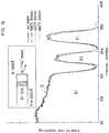
- Fig. 16 is a graph indicating the result of analysis four samples as follows by RBS (Rutherford Backscattering Spectroscopy); a TiN film of 1000 ⁇ formed on a Si substrate, with Al deposited thereon, (1) unheated, (2) heated at 500 °C for 30 minutes, (3) at 600 °C for 30 minutes, and (4) at 650°C for 30 minutes.
- RBS comprises the steps of irradiating He atoms of a definite energy on the substrate, and by the energy of the reflecting He investigating the element distribution to the direction of the film thickness in the film.
- the energy loss of He which collided with every element is determined by element (atomic weight), that is, the lighter the element is, the lighter it goes.
- the peaks come in the order of Si, Ti, and Al. Besides, the width of each peak corresponds to the film thickness, so that a wide peak means diffusion (as Si is a substrate and wide, only the one side can be seen). It is obvious from Fig. 16 that the peaks make almost no change by heat treatment, and that even after the heat treatment at 650°C for 30 minutes, it shows high barrier characteristic (effect of preventing diffusion).
- a diagram at the upper part in the frame indicates that in the film structure Al/TiN/Si, He was irradiated from the direction of Al, and the yield of He ions scattering backward was measured.
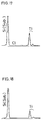
- Figs. 17 and 18 shows the EDX (Energy Dispersion-type X-ray analyzer) spectra of the TiN films formed at the microwave power of 1kw and 2.8kw, under the same deposition conditions as those in the examples according to the present invention.
- the microwave power of 1kw the peak of chlorine Cl was noticed, while at 2.8kw no peak of chlorine Cl was noticed.
- chlorine Cl can be reduced by the H2 plasma treatment after the TiN film formation.
- Fig. 19 indicates the result analyzed by SIMS (Secondary Ion Mass Spectroscopy) from the surface of the sample given the H2 plasma treatment after the TiN film formation to the direction of depth (vertically to TiN film toward the Si substrate).
- the SIMS comprises the steps of digging the film to the direction of depth by irradiating oxygen ions and measuring the distribution of elements or molecules (e.g. TiN) existing in the direction of the depth.
- elements or molecules e.g. TiN
- the left side (on the vertical axis) is the surface side of a TiN film, and as going to the right, the depth digged down becomes bigger.
- chlorine was reduced by the H2 plasma treatment after the TiN film formation.
- the H2 plasma treatment is to stop supplying Ti compound gas such as TiCl4 and N2 gas at the end of the treatment of the TiN film formation, and to supply Ar gas and H2 gas in order to keep the state wherein a plasma is produced.
- X-ray diffraction pattern of TiN film formed by the method according to the example is shown in Fig. 20.
- the pattern diagram indicates the crystal of TiN oriented on the Si substrate (111) only in the direction (100).
- the deposition conditions were microwave power 1kw, substrate temperature 550°C, flow of N2: 15 SCCM, H2: 50 SCCM, and Ar: 43 SCCM.
- (100) oriented film has an excellent barrier characteristic, and it is guessed that extremely strong (100) orientation of a TiN film formed by the method according to the example may be based on the directionality of a plasma.
- the method for forming a thin film according to the present invention is capable of forming a metal nitride film having good Step Coverage, and forming a thin film sufficiently keeping a barrier characteristic on the contact hole, even if a LSI device gets more highly integrated and aspect ratio of the contact hole formed on a insulation layer becomes bigger.
- the film thickness of the thin film formed on the side wall of the contact hole can be made thinner than that on the bottom of the contact hole, and with keeping a barrier characteristic on the bottom of the contact hole, aspect ratio of the contact hole after forming a thin film can be refrained from enhanced. Accordingly, in the following step of filling in with interconnection materials, no voids occur in the contact hole, resulting in preventing interconnection from broken and improving reliability of a LSI device.
Landscapes
- Electrodes Of Semiconductors (AREA)
- Internal Circuitry In Semiconductor Integrated Circuit Devices (AREA)
- Chemical Vapour Deposition (AREA)
Applications Claiming Priority (4)
| Application Number | Priority Date | Filing Date | Title |
|---|---|---|---|
| JP28776590 | 1990-10-24 | ||
| JP287765/90 | 1990-10-24 | ||
| JP16236591 | 1991-06-07 | ||
| JP162365/91 | 1991-06-07 |
Publications (3)
| Publication Number | Publication Date |
|---|---|
| EP0483669A2 true EP0483669A2 (de) | 1992-05-06 |
| EP0483669A3 EP0483669A3 (en) | 1992-12-23 |
| EP0483669B1 EP0483669B1 (de) | 1996-06-19 |
Family
ID=26488181
Family Applications (1)
| Application Number | Title | Priority Date | Filing Date |
|---|---|---|---|
| EP91118166A Expired - Lifetime EP0483669B1 (de) | 1990-10-24 | 1991-10-24 | Verfahren zur Herstellung einer dünnen Schicht und Halbleitervorrichtungen |
Country Status (4)
| Country | Link |
|---|---|
| US (1) | US5296404A (de) |
| EP (1) | EP0483669B1 (de) |
| KR (1) | KR100228259B1 (de) |
| DE (1) | DE69120371T2 (de) |
Cited By (3)
| Publication number | Priority date | Publication date | Assignee | Title |
|---|---|---|---|---|
| FR2709207A1 (fr) * | 1993-08-19 | 1995-02-24 | Ind Technology Research | Procédé de métallisation d'un circuit intégré. |
| US7093559B2 (en) * | 1999-02-12 | 2006-08-22 | Micron Technology, Inc. | Method for PECVD deposition of selected material films |
| CN103938272A (zh) * | 2014-04-03 | 2014-07-23 | 清华大学 | 等离子体辅助的外延生长装置及方法 |
Families Citing this family (41)
| Publication number | Priority date | Publication date | Assignee | Title |
|---|---|---|---|---|
| US5300813A (en) * | 1992-02-26 | 1994-04-05 | International Business Machines Corporation | Refractory metal capped low resistivity metal conductor lines and vias |
| KR950009934B1 (ko) * | 1992-09-07 | 1995-09-01 | 삼성전자주식회사 | 반도체 장치의 배선층 형성방법 |
| JPH0741948A (ja) * | 1993-07-30 | 1995-02-10 | Sony Corp | 配線形成方法 |
| JP3395299B2 (ja) * | 1993-11-08 | 2003-04-07 | ソニー株式会社 | 半導体装置の配線構造及び配線形成方法 |
| US5420072A (en) * | 1994-02-04 | 1995-05-30 | Motorola, Inc. | Method for forming a conductive interconnect in an integrated circuit |
| US5665640A (en) | 1994-06-03 | 1997-09-09 | Sony Corporation | Method for producing titanium-containing thin films by low temperature plasma-enhanced chemical vapor deposition using a rotating susceptor reactor |
| US5975912A (en) * | 1994-06-03 | 1999-11-02 | Materials Research Corporation | Low temperature plasma-enhanced formation of integrated circuits |
| US5628829A (en) | 1994-06-03 | 1997-05-13 | Materials Research Corporation | Method and apparatus for low temperature deposition of CVD and PECVD films |
| AU1745695A (en) | 1994-06-03 | 1996-01-04 | Materials Research Corporation | A method of nitridization of titanium thin films |
| KR0144956B1 (ko) * | 1994-06-10 | 1998-08-17 | 김광호 | 반도체 장치의 배선 구조 및 그 형성방법 |
| US5621607A (en) * | 1994-10-07 | 1997-04-15 | Maxwell Laboratories, Inc. | High performance double layer capacitors including aluminum carbon composite electrodes |
| US6291343B1 (en) * | 1994-11-14 | 2001-09-18 | Applied Materials, Inc. | Plasma annealing of substrates to improve adhesion |
| US5571576A (en) * | 1995-02-10 | 1996-11-05 | Watkins-Johnson | Method of forming a fluorinated silicon oxide layer using plasma chemical vapor deposition |
| US5610106A (en) * | 1995-03-10 | 1997-03-11 | Sony Corporation | Plasma enhanced chemical vapor deposition of titanium nitride using ammonia |
| US5567483A (en) * | 1995-06-05 | 1996-10-22 | Sony Corporation | Process for plasma enhanced anneal of titanium nitride |
| US5661083A (en) * | 1996-01-30 | 1997-08-26 | Integrated Device Technology, Inc. | Method for via formation with reduced contact resistance |
| US5956608A (en) * | 1996-06-20 | 1999-09-21 | Applied Materials, Inc. | Modulating surface morphology of barrier layers |
| US5801098A (en) * | 1996-09-03 | 1998-09-01 | Motorola, Inc. | Method of decreasing resistivity in an electrically conductive layer |
| TW314654B (en) * | 1996-09-07 | 1997-09-01 | United Microelectronics Corp | Manufacturing method of conductive plug |
| US6025269A (en) * | 1996-10-15 | 2000-02-15 | Micron Technology, Inc. | Method for depositioning a substantially void-free aluminum film over a refractory metal nitride layer |
| EP0854505A3 (de) * | 1997-01-21 | 1998-11-11 | Texas Instruments Incorporated | Abscheidungsverfahren von einer Schicht auf der Basis von TiN während der Herstellung einer Halbleitervorrichtung |
| US5989652A (en) * | 1997-01-31 | 1999-11-23 | Tokyo Electron Limited | Method of low temperature plasma enhanced chemical vapor deposition of tin film over titanium for use in via level applications |
| US6872429B1 (en) | 1997-06-30 | 2005-03-29 | Applied Materials, Inc. | Deposition of tungsten nitride using plasma pretreatment in a chemical vapor deposition chamber |
| US6432479B2 (en) | 1997-12-02 | 2002-08-13 | Applied Materials, Inc. | Method for in-situ, post deposition surface passivation of a chemical vapor deposited film |
| US5962344A (en) * | 1997-12-29 | 1999-10-05 | Vanguard International Semiconductor Corporation | Plasma treatment method for PECVD silicon nitride films for improved passivation layers on semiconductor metal interconnections |
| US6635569B1 (en) * | 1998-04-20 | 2003-10-21 | Tokyo Electron Limited | Method of passivating and stabilizing a Ti-PECVD process chamber and combined Ti-PECVD/TiN-CVD processing method and apparatus |
| US6319728B1 (en) | 1998-06-05 | 2001-11-20 | Applied Materials, Inc. | Method for treating a deposited film for resistivity reduction |
| US6100185A (en) * | 1998-08-14 | 2000-08-08 | Micron Technology, Inc. | Semiconductor processing method of forming a high purity <200> grain orientation tin layer and semiconductor processing method of forming a conductive interconnect line |
| US6245674B1 (en) | 1999-03-01 | 2001-06-12 | Micron Technology, Inc. | Method of forming a metal silicide comprising contact over a substrate |
| US6365507B1 (en) | 1999-03-01 | 2002-04-02 | Micron Technology, Inc. | Method of forming integrated circuitry |
| US6524951B2 (en) * | 1999-03-01 | 2003-02-25 | Micron Technology, Inc. | Method of forming a silicide interconnect over a silicon comprising substrate and method of forming a stack of refractory metal nitride over refractory metal silicide over silicon |
| EP1090417A1 (de) | 1999-04-20 | 2001-04-11 | Tokyo Electron Limited | Verfahren zur herstellung von pecvd-titanschichten und cvd-titannitridschichten für integrierte schaltungen in ein und derselben reaktionskammer |
| US6555183B2 (en) * | 1999-06-11 | 2003-04-29 | Applied Materials, Inc. | Plasma treatment of a titanium nitride film formed by chemical vapor deposition |
| US6821571B2 (en) * | 1999-06-18 | 2004-11-23 | Applied Materials Inc. | Plasma treatment to enhance adhesion and to minimize oxidation of carbon-containing layers |
| US6541369B2 (en) | 1999-12-07 | 2003-04-01 | Applied Materials, Inc. | Method and apparatus for reducing fixed charges in a semiconductor device |
| JP2001298028A (ja) * | 2000-04-17 | 2001-10-26 | Tokyo Electron Ltd | 半導体デバイス製造方法 |
| EP2221864B1 (de) * | 2005-12-02 | 2018-04-11 | Ulvac, Inc. | Verfahren zur Herstellung eines Kupferfilms |
| WO2007092835A2 (en) | 2006-02-07 | 2007-08-16 | William Marsh Rice University | Production de reseaux verticaux de nanotubes de carbone a petit diametre et paroi simple |
| US20080235944A1 (en) * | 2007-03-31 | 2008-10-02 | John Miller | Method of making a corrugated electrode core terminal interface |
| US20080241656A1 (en) * | 2007-03-31 | 2008-10-02 | John Miller | Corrugated electrode core terminal interface apparatus and article of manufacture |
| JP2021136273A (ja) | 2020-02-25 | 2021-09-13 | キオクシア株式会社 | 半導体装置およびその製造方法 |
Family Cites Families (6)
| Publication number | Priority date | Publication date | Assignee | Title |
|---|---|---|---|---|
| CA1159012A (en) * | 1980-05-02 | 1983-12-20 | Seitaro Matsuo | Plasma deposition apparatus |
| US4570328A (en) * | 1983-03-07 | 1986-02-18 | Motorola, Inc. | Method of producing titanium nitride MOS device gate electrode |
| US4973883A (en) * | 1987-05-01 | 1990-11-27 | Semiconductor Energy Laborator Co., Ltd. | Plasma processing apparatus with a lisitano coil |
| JPS63299251A (ja) * | 1987-05-29 | 1988-12-06 | Toshiba Corp | 半導体装置の製造方法 |
| US4878994A (en) * | 1987-07-16 | 1989-11-07 | Texas Instruments Incorporated | Method for etching titanium nitride local interconnects |
| JP2747036B2 (ja) * | 1989-07-07 | 1998-05-06 | 日本電信電話株式会社 | 薄膜形成方法 |
-
1991
- 1991-10-23 KR KR1019910018675A patent/KR100228259B1/ko not_active Expired - Fee Related
- 1991-10-24 EP EP91118166A patent/EP0483669B1/de not_active Expired - Lifetime
- 1991-10-24 US US07/779,497 patent/US5296404A/en not_active Expired - Fee Related
- 1991-10-24 DE DE69120371T patent/DE69120371T2/de not_active Expired - Fee Related
Cited By (3)
| Publication number | Priority date | Publication date | Assignee | Title |
|---|---|---|---|---|
| FR2709207A1 (fr) * | 1993-08-19 | 1995-02-24 | Ind Technology Research | Procédé de métallisation d'un circuit intégré. |
| US7093559B2 (en) * | 1999-02-12 | 2006-08-22 | Micron Technology, Inc. | Method for PECVD deposition of selected material films |
| CN103938272A (zh) * | 2014-04-03 | 2014-07-23 | 清华大学 | 等离子体辅助的外延生长装置及方法 |
Also Published As
| Publication number | Publication date |
|---|---|
| DE69120371T2 (de) | 1997-02-06 |
| KR100228259B1 (ko) | 1999-11-01 |
| EP0483669B1 (de) | 1996-06-19 |
| US5296404A (en) | 1994-03-22 |
| KR920008852A (ko) | 1992-05-28 |
| DE69120371D1 (de) | 1996-07-25 |
| EP0483669A3 (en) | 1992-12-23 |
Similar Documents
| Publication | Publication Date | Title |
|---|---|---|
| EP0483669B1 (de) | Verfahren zur Herstellung einer dünnen Schicht und Halbleitervorrichtungen | |
| EP0536664B1 (de) | Verfahren zur Bildung eines dünnen Films | |
| US6251758B1 (en) | Construction of a film on a semiconductor wafer | |
| US6699530B2 (en) | Method for constructing a film on a semiconductor wafer | |
| US5989999A (en) | Construction of a tantalum nitride film on a semiconductor wafer | |
| US6841044B1 (en) | Chemically-enhanced physical vapor deposition | |
| US9255329B2 (en) | Modulated ion-induced atomic layer deposition (MII-ALD) | |
| EP1094504A2 (de) | Durch PVD-IMP abgeschiedenes Wolfram und Wolframnitrid als Auskleidungs-, Barriere- oder Keimschicht | |
| US20010002326A1 (en) | Metal and metal silicide nitridization in a high density, low pressure plasma reactor | |
| KR100247515B1 (ko) | 플라즈마 cvd에 의한 박막형성방법 | |
| EP1033746A1 (de) | Plasma-abscheidung eines films | |
| EP0776991B1 (de) | Plasmatempern von Dünnschichten | |
| EP1035568A1 (de) | Plasma-Verfahren | |
| US6337290B1 (en) | Semiconductor device having fluorine-added carbon dielectric film and method of fabricating the same | |
| Cerio et al. | Film properties of Ti/TiN bilayers deposited sequentially by ionized physical vapor deposition | |
| JP3243722B2 (ja) | 薄膜の形成方法および半導体装置 | |
| JP3063519B2 (ja) | 薄膜の形成方法 | |
| Chiang et al. | Ion-induced chemical vapor deposition of high purity Cu films at room temperature using a microwave discharge H atom beam source | |
| JP4454675B2 (ja) | ウェハ上に窒化メタル膜を構築する方法 | |
| Ono et al. | Tantalum and tantalum nitride films deposited by electron cyclotron resonance sputtering as barriers to copper diffusion | |
| KR100542799B1 (ko) | 반도체웨이퍼상에서막을형성하는방법 | |
| JP3413276B2 (ja) | 薄膜の形成方法 | |
| Mahowald et al. | Plasma-enhanced chemical vapor deposition of tungsten | |
| Collings | Electron Enhanced Atomic Layer Deposition (EE-ALD) of Ruthenium and Controlled Electron Enhanced Etching of Molybdenum and Monoclinic Gallium Oxide | |
| JPH11256318A (ja) | 導電性薄膜及びその形成方法、並びに、半導体装置及びその製造方法 |
Legal Events
| Date | Code | Title | Description |
|---|---|---|---|
| PUAI | Public reference made under article 153(3) epc to a published international application that has entered the european phase |
Free format text: ORIGINAL CODE: 0009012 |
|
| AK | Designated contracting states |
Kind code of ref document: A2 Designated state(s): DE FR GB NL |
|
| 17P | Request for examination filed |
Effective date: 19920702 |
|
| PUAL | Search report despatched |
Free format text: ORIGINAL CODE: 0009013 |
|
| AK | Designated contracting states |
Kind code of ref document: A3 Designated state(s): DE FR GB NL |
|
| 17Q | First examination report despatched |
Effective date: 19940310 |
|
| GRAH | Despatch of communication of intention to grant a patent |
Free format text: ORIGINAL CODE: EPIDOS IGRA |
|
| GRAH | Despatch of communication of intention to grant a patent |
Free format text: ORIGINAL CODE: EPIDOS IGRA |
|
| GRAA | (expected) grant |
Free format text: ORIGINAL CODE: 0009210 |
|
| AK | Designated contracting states |
Kind code of ref document: B1 Designated state(s): DE FR GB NL |
|
| REF | Corresponds to: |
Ref document number: 69120371 Country of ref document: DE Date of ref document: 19960725 |
|
| ET | Fr: translation filed | ||
| NLT2 | Nl: modifications (of names), taken from the european patent patent bulletin |
Owner name: SUMITOMO METAL INDUSTRIES, LTD. |
|
| PLBE | No opposition filed within time limit |
Free format text: ORIGINAL CODE: 0009261 |
|
| STAA | Information on the status of an ep patent application or granted ep patent |
Free format text: STATUS: NO OPPOSITION FILED WITHIN TIME LIMIT |
|
| 26N | No opposition filed | ||
| REG | Reference to a national code |
Ref country code: GB Ref legal event code: IF02 |
|
| PGFP | Annual fee paid to national office [announced via postgrant information from national office to epo] |
Ref country code: FR Payment date: 20021008 Year of fee payment: 12 |
|
| PGFP | Annual fee paid to national office [announced via postgrant information from national office to epo] |
Ref country code: GB Payment date: 20021023 Year of fee payment: 12 |
|
| PGFP | Annual fee paid to national office [announced via postgrant information from national office to epo] |
Ref country code: DE Payment date: 20021024 Year of fee payment: 12 |
|
| PGFP | Annual fee paid to national office [announced via postgrant information from national office to epo] |
Ref country code: NL Payment date: 20021031 Year of fee payment: 12 |
|
| REG | Reference to a national code |
Ref country code: GB Ref legal event code: 732E |
|
| REG | Reference to a national code |
Ref country code: FR Ref legal event code: TP |
|
| NLS | Nl: assignments of ep-patents |
Owner name: TOKYO ELECTRON LIMITED |
|
| PG25 | Lapsed in a contracting state [announced via postgrant information from national office to epo] |
Ref country code: GB Free format text: LAPSE BECAUSE OF NON-PAYMENT OF DUE FEES Effective date: 20031024 |
|
| PG25 | Lapsed in a contracting state [announced via postgrant information from national office to epo] |
Ref country code: NL Free format text: LAPSE BECAUSE OF NON-PAYMENT OF DUE FEES Effective date: 20040501 Ref country code: DE Free format text: LAPSE BECAUSE OF NON-PAYMENT OF DUE FEES Effective date: 20040501 |
|
| GBPC | Gb: european patent ceased through non-payment of renewal fee |
Effective date: 20031024 |
|
| PG25 | Lapsed in a contracting state [announced via postgrant information from national office to epo] |
Ref country code: FR Free format text: LAPSE BECAUSE OF NON-PAYMENT OF DUE FEES Effective date: 20040630 |
|
| NLV4 | Nl: lapsed or anulled due to non-payment of the annual fee |
Effective date: 20040501 |
|
| REG | Reference to a national code |
Ref country code: FR Ref legal event code: ST |