EP0483687A2 - Optische Vorrichtung mit asymmetrischer Doppel-Quantumwell-Struktur - Google Patents
Optische Vorrichtung mit asymmetrischer Doppel-Quantumwell-Struktur Download PDFInfo
- Publication number
- EP0483687A2 EP0483687A2 EP91118250A EP91118250A EP0483687A2 EP 0483687 A2 EP0483687 A2 EP 0483687A2 EP 91118250 A EP91118250 A EP 91118250A EP 91118250 A EP91118250 A EP 91118250A EP 0483687 A2 EP0483687 A2 EP 0483687A2
- Authority
- EP
- European Patent Office
- Prior art keywords
- quantum well
- electric field
- layer
- optical device
- wavelength
- Prior art date
- Legal status (The legal status is an assumption and is not a legal conclusion. Google has not performed a legal analysis and makes no representation as to the accuracy of the status listed.)
- Granted
Links
- 230000003287 optical effect Effects 0.000 title claims abstract description 20
- 230000009977 dual effect Effects 0.000 title claims abstract description 12
- 230000005684 electric field Effects 0.000 claims abstract description 60
- 230000005701 quantum confined stark effect Effects 0.000 claims abstract description 10
- 239000004065 semiconductor Substances 0.000 claims abstract description 10
- 230000004888 barrier function Effects 0.000 claims description 3
- 238000010521 absorption reaction Methods 0.000 abstract description 20
- 239000000758 substrate Substances 0.000 description 10
- 230000005428 wave function Effects 0.000 description 10
- 230000007423 decrease Effects 0.000 description 8
- 230000007704 transition Effects 0.000 description 7
- 229910001218 Gallium arsenide Inorganic materials 0.000 description 6
- 230000001105 regulatory effect Effects 0.000 description 4
- 238000002347 injection Methods 0.000 description 3
- 239000007924 injection Substances 0.000 description 3
- 230000000644 propagated effect Effects 0.000 description 3
- 230000002441 reversible effect Effects 0.000 description 3
- 238000001228 spectrum Methods 0.000 description 3
- 230000002269 spontaneous effect Effects 0.000 description 3
- VYPSYNLAJGMNEJ-UHFFFAOYSA-N Silicium dioxide Chemical compound O=[Si]=O VYPSYNLAJGMNEJ-UHFFFAOYSA-N 0.000 description 2
- GWEVSGVZZGPLCZ-UHFFFAOYSA-N Titan oxide Chemical compound O=[Ti]=O GWEVSGVZZGPLCZ-UHFFFAOYSA-N 0.000 description 2
- 230000003321 amplification Effects 0.000 description 2
- 239000000969 carrier Substances 0.000 description 2
- 230000008859 change Effects 0.000 description 2
- 238000010586 diagram Methods 0.000 description 2
- 239000002019 doping agent Substances 0.000 description 2
- 238000001914 filtration Methods 0.000 description 2
- 238000003199 nucleic acid amplification method Methods 0.000 description 2
- 239000013307 optical fiber Substances 0.000 description 2
- 239000010409 thin film Substances 0.000 description 2
- 229910000980 Aluminium gallium arsenide Inorganic materials 0.000 description 1
- 229910004205 SiNX Inorganic materials 0.000 description 1
- 230000002411 adverse Effects 0.000 description 1
- 230000005540 biological transmission Effects 0.000 description 1
- 229910052681 coesite Inorganic materials 0.000 description 1
- 230000001427 coherent effect Effects 0.000 description 1
- 229910052906 cristobalite Inorganic materials 0.000 description 1
- 230000000694 effects Effects 0.000 description 1
- 239000010408 film Substances 0.000 description 1
- 230000003993 interaction Effects 0.000 description 1
- 239000000463 material Substances 0.000 description 1
- 230000004048 modification Effects 0.000 description 1
- 238000012986 modification Methods 0.000 description 1
- 230000010355 oscillation Effects 0.000 description 1
- 230000010363 phase shift Effects 0.000 description 1
- 230000005855 radiation Effects 0.000 description 1
- 239000000377 silicon dioxide Substances 0.000 description 1
- 235000012239 silicon dioxide Nutrition 0.000 description 1
- 230000000087 stabilizing effect Effects 0.000 description 1
- 229910052682 stishovite Inorganic materials 0.000 description 1
- 238000000411 transmission spectrum Methods 0.000 description 1
- 229910052905 tridymite Inorganic materials 0.000 description 1
Images


Classifications
-
- G—PHYSICS
- G02—OPTICS
- G02F—OPTICAL DEVICES OR ARRANGEMENTS FOR THE CONTROL OF LIGHT BY MODIFICATION OF THE OPTICAL PROPERTIES OF THE MEDIA OF THE ELEMENTS INVOLVED THEREIN; NON-LINEAR OPTICS; FREQUENCY-CHANGING OF LIGHT; OPTICAL LOGIC ELEMENTS; OPTICAL ANALOGUE/DIGITAL CONVERTERS
- G02F1/00—Devices or arrangements for the control of the intensity, colour, phase, polarisation or direction of light arriving from an independent light source, e.g. switching, gating or modulating; Non-linear optics
- G02F1/01—Devices or arrangements for the control of the intensity, colour, phase, polarisation or direction of light arriving from an independent light source, e.g. switching, gating or modulating; Non-linear optics for the control of the intensity, phase, polarisation or colour
- G02F1/015—Devices or arrangements for the control of the intensity, colour, phase, polarisation or direction of light arriving from an independent light source, e.g. switching, gating or modulating; Non-linear optics for the control of the intensity, phase, polarisation or colour based on semiconductor elements having potential barriers, e.g. having a PN or PIN junction
- G02F1/017—Structures with periodic or quasi periodic potential variation, e.g. superlattices, quantum wells
- G02F1/01725—Non-rectangular quantum well structures, e.g. graded or stepped quantum wells
-
- B—PERFORMING OPERATIONS; TRANSPORTING
- B82—NANOTECHNOLOGY
- B82Y—SPECIFIC USES OR APPLICATIONS OF NANOSTRUCTURES; MEASUREMENT OR ANALYSIS OF NANOSTRUCTURES; MANUFACTURE OR TREATMENT OF NANOSTRUCTURES
- B82Y20/00—Nanooptics, e.g. quantum optics or photonic crystals
-
- H—ELECTRICITY
- H01—ELECTRIC ELEMENTS
- H01S—DEVICES USING THE PROCESS OF LIGHT AMPLIFICATION BY STIMULATED EMISSION OF RADIATION [LASER] TO AMPLIFY OR GENERATE LIGHT; DEVICES USING STIMULATED EMISSION OF ELECTROMAGNETIC RADIATION IN WAVE RANGES OTHER THAN OPTICAL
- H01S5/00—Semiconductor lasers
- H01S5/30—Structure or shape of the active region; Materials used for the active region
- H01S5/34—Structure or shape of the active region; Materials used for the active region comprising quantum well or superlattice structures, e.g. single quantum well [SQW] lasers, multiple quantum well [MQW] lasers or graded index separate confinement heterostructure [GRINSCH] lasers
-
- H—ELECTRICITY
- H01—ELECTRIC ELEMENTS
- H01S—DEVICES USING THE PROCESS OF LIGHT AMPLIFICATION BY STIMULATED EMISSION OF RADIATION [LASER] TO AMPLIFY OR GENERATE LIGHT; DEVICES USING STIMULATED EMISSION OF ELECTROMAGNETIC RADIATION IN WAVE RANGES OTHER THAN OPTICAL
- H01S5/00—Semiconductor lasers
- H01S5/50—Amplifier structures not provided for in groups H01S5/02 - H01S5/30
- H01S5/5045—Amplifier structures not provided for in groups H01S5/02 - H01S5/30 the arrangement having a frequency filtering function
-
- G—PHYSICS
- G02—OPTICS
- G02F—OPTICAL DEVICES OR ARRANGEMENTS FOR THE CONTROL OF LIGHT BY MODIFICATION OF THE OPTICAL PROPERTIES OF THE MEDIA OF THE ELEMENTS INVOLVED THEREIN; NON-LINEAR OPTICS; FREQUENCY-CHANGING OF LIGHT; OPTICAL LOGIC ELEMENTS; OPTICAL ANALOGUE/DIGITAL CONVERTERS
- G02F1/00—Devices or arrangements for the control of the intensity, colour, phase, polarisation or direction of light arriving from an independent light source, e.g. switching, gating or modulating; Non-linear optics
- G02F1/01—Devices or arrangements for the control of the intensity, colour, phase, polarisation or direction of light arriving from an independent light source, e.g. switching, gating or modulating; Non-linear optics for the control of the intensity, phase, polarisation or colour
- G02F1/015—Devices or arrangements for the control of the intensity, colour, phase, polarisation or direction of light arriving from an independent light source, e.g. switching, gating or modulating; Non-linear optics for the control of the intensity, phase, polarisation or colour based on semiconductor elements having potential barriers, e.g. having a PN or PIN junction
- G02F1/0151—Devices or arrangements for the control of the intensity, colour, phase, polarisation or direction of light arriving from an independent light source, e.g. switching, gating or modulating; Non-linear optics for the control of the intensity, phase, polarisation or colour based on semiconductor elements having potential barriers, e.g. having a PN or PIN junction modulating the refractive index
-
- G—PHYSICS
- G02—OPTICS
- G02F—OPTICAL DEVICES OR ARRANGEMENTS FOR THE CONTROL OF LIGHT BY MODIFICATION OF THE OPTICAL PROPERTIES OF THE MEDIA OF THE ELEMENTS INVOLVED THEREIN; NON-LINEAR OPTICS; FREQUENCY-CHANGING OF LIGHT; OPTICAL LOGIC ELEMENTS; OPTICAL ANALOGUE/DIGITAL CONVERTERS
- G02F1/00—Devices or arrangements for the control of the intensity, colour, phase, polarisation or direction of light arriving from an independent light source, e.g. switching, gating or modulating; Non-linear optics
- G02F1/01—Devices or arrangements for the control of the intensity, colour, phase, polarisation or direction of light arriving from an independent light source, e.g. switching, gating or modulating; Non-linear optics for the control of the intensity, phase, polarisation or colour
- G02F1/015—Devices or arrangements for the control of the intensity, colour, phase, polarisation or direction of light arriving from an independent light source, e.g. switching, gating or modulating; Non-linear optics for the control of the intensity, phase, polarisation or colour based on semiconductor elements having potential barriers, e.g. having a PN or PIN junction
- G02F1/017—Structures with periodic or quasi periodic potential variation, e.g. superlattices, quantum wells
- G02F1/01708—Structures with periodic or quasi periodic potential variation, e.g. superlattices, quantum wells in an optical wavequide structure
-
- G—PHYSICS
- G02—OPTICS
- G02F—OPTICAL DEVICES OR ARRANGEMENTS FOR THE CONTROL OF LIGHT BY MODIFICATION OF THE OPTICAL PROPERTIES OF THE MEDIA OF THE ELEMENTS INVOLVED THEREIN; NON-LINEAR OPTICS; FREQUENCY-CHANGING OF LIGHT; OPTICAL LOGIC ELEMENTS; OPTICAL ANALOGUE/DIGITAL CONVERTERS
- G02F1/00—Devices or arrangements for the control of the intensity, colour, phase, polarisation or direction of light arriving from an independent light source, e.g. switching, gating or modulating; Non-linear optics
- G02F1/01—Devices or arrangements for the control of the intensity, colour, phase, polarisation or direction of light arriving from an independent light source, e.g. switching, gating or modulating; Non-linear optics for the control of the intensity, phase, polarisation or colour
- G02F1/015—Devices or arrangements for the control of the intensity, colour, phase, polarisation or direction of light arriving from an independent light source, e.g. switching, gating or modulating; Non-linear optics for the control of the intensity, phase, polarisation or colour based on semiconductor elements having potential barriers, e.g. having a PN or PIN junction
- G02F1/017—Structures with periodic or quasi periodic potential variation, e.g. superlattices, quantum wells
- G02F1/01725—Non-rectangular quantum well structures, e.g. graded or stepped quantum wells
- G02F1/01733—Coupled or double quantum wells
- G02F1/01741—Asymmetrically coupled or double quantum wells
-
- G—PHYSICS
- G02—OPTICS
- G02F—OPTICAL DEVICES OR ARRANGEMENTS FOR THE CONTROL OF LIGHT BY MODIFICATION OF THE OPTICAL PROPERTIES OF THE MEDIA OF THE ELEMENTS INVOLVED THEREIN; NON-LINEAR OPTICS; FREQUENCY-CHANGING OF LIGHT; OPTICAL LOGIC ELEMENTS; OPTICAL ANALOGUE/DIGITAL CONVERTERS
- G02F2201/00—Constructional arrangements not provided for in groups G02F1/00 - G02F7/00
- G02F2201/30—Constructional arrangements not provided for in groups G02F1/00 - G02F7/00 grating
- G02F2201/307—Reflective grating, i.e. Bragg grating
-
- G—PHYSICS
- G02—OPTICS
- G02F—OPTICAL DEVICES OR ARRANGEMENTS FOR THE CONTROL OF LIGHT BY MODIFICATION OF THE OPTICAL PROPERTIES OF THE MEDIA OF THE ELEMENTS INVOLVED THEREIN; NON-LINEAR OPTICS; FREQUENCY-CHANGING OF LIGHT; OPTICAL LOGIC ELEMENTS; OPTICAL ANALOGUE/DIGITAL CONVERTERS
- G02F2203/00—Function characteristic
- G02F2203/05—Function characteristic wavelength dependent
- G02F2203/055—Function characteristic wavelength dependent wavelength filtering
-
- H—ELECTRICITY
- H01—ELECTRIC ELEMENTS
- H01S—DEVICES USING THE PROCESS OF LIGHT AMPLIFICATION BY STIMULATED EMISSION OF RADIATION [LASER] TO AMPLIFY OR GENERATE LIGHT; DEVICES USING STIMULATED EMISSION OF ELECTROMAGNETIC RADIATION IN WAVE RANGES OTHER THAN OPTICAL
- H01S5/00—Semiconductor lasers
- H01S5/06—Arrangements for controlling the laser output parameters, e.g. by operating on the active medium
- H01S5/062—Arrangements for controlling the laser output parameters, e.g. by operating on the active medium by varying the potential of the electrodes
- H01S5/06203—Transistor-type lasers
- H01S5/06206—Controlling the frequency of the radiation, e.g. tunable twin-guide lasers [TTG]
-
- H—ELECTRICITY
- H01—ELECTRIC ELEMENTS
- H01S—DEVICES USING THE PROCESS OF LIGHT AMPLIFICATION BY STIMULATED EMISSION OF RADIATION [LASER] TO AMPLIFY OR GENERATE LIGHT; DEVICES USING STIMULATED EMISSION OF ELECTROMAGNETIC RADIATION IN WAVE RANGES OTHER THAN OPTICAL
- H01S5/00—Semiconductor lasers
- H01S5/30—Structure or shape of the active region; Materials used for the active region
- H01S5/34—Structure or shape of the active region; Materials used for the active region comprising quantum well or superlattice structures, e.g. single quantum well [SQW] lasers, multiple quantum well [MQW] lasers or graded index separate confinement heterostructure [GRINSCH] lasers
- H01S5/3408—Structure or shape of the active region; Materials used for the active region comprising quantum well or superlattice structures, e.g. single quantum well [SQW] lasers, multiple quantum well [MQW] lasers or graded index separate confinement heterostructure [GRINSCH] lasers characterised by specially shaped wells, e.g. triangular
Definitions
- This invention relates to optical devices in which a semiconductor quantum well structure is formed as an asymmetric dual quantum well (ADQW) structure including a plurality of different quantum wells (typically two wells) for achieving a specific property.
- a semiconductor quantum well structure is formed as an asymmetric dual quantum well (ADQW) structure including a plurality of different quantum wells (typically two wells) for achieving a specific property.
- ADQW asymmetric dual quantum well
- wavelength division multiplexing systems if semiconductor lasers are used as a light source, a wavelength range of tunable or changeable radiation lights is at most several tens ⁇ , so that when the wavelength division multiplexing communication is conducted within such wavelength range, devices for selecting or filtering light having a wavelength spectrum width less than 1 ⁇ at a resolution of 2 ⁇ 3 ⁇ are required.
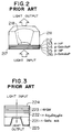
- Fig. 1 shows the structure of a waveguide type filter including a distributed reflector portion which is an example of the above-mentioned devices (see.
- a waveguide 202 with a grating 203 and a partial active layer 204 there are provided, on a substrate 201, a waveguide 202 with a grating 203 and a partial active layer 204.
- the device is divided into two active portions 205a and 205b including the active layer 204 and a phase regulating portion 206 without the active layer 204 formed therebetween.
- Anti-reflection coats 207a and 207b made of SiN x are deposited on both end surfaces of the device.
- Reference letters N a , N p and ⁇ respectively denote refractive indices of the waveguide 202 in the active portions 205a and 205b and the phase regulating portion 206 and the length of the phase regulating portion 206.
- the refractive indices N a and N p in the waveguide 202 are changed by injecting an active current I a and a phase regulating current I p into the respective portions 205a, 205b and 206 to vary carrier densities in the waveguide 202 thereat.
- the wavelength of light reflected by the grating 203 or distributed reflector structure is varied to achieve a tunable filter.
- Such tunable filter has drawbacks that a decrease of refractive index resulting from the carrier injection into the waveguide is reduced by an increase of refractive index resulting from a raise of temperature due to current flowing in the waveguide 202 and that thermal noise also occurs due to such raise of temperature.
- a decrease of refractive index resulting from the carrier injection into the waveguide is reduced by an increase of refractive index resulting from a raise of temperature due to current flowing in the waveguide 202 and that thermal noise also occurs due to such raise of temperature.
- spontaneous emission appears due to the carrier injection, that a beat noise occurs from interaction between the spontaneous emission and an incident light, and others.
- Fig. 2 shows another prior art example which is a filter of Fabry-Perot type using a structure similar to surface emission type lasers (see Kubota et al.: Tunable filter of surface emission laser type, Informal Paper No. C-246 distributed at Vernal Grand Meeting of Electronics Information Commun. Academy (1990)).
- etch-stop layer 212 on a substrate 211, an etch-stop layer 212 and layers 213, 214, 215 and 216 of n-InP, p-GaInAsP, p-InP and p-GaInAsP.
- Anti-reflection coats 217 and 218 of TiO2/SiO2 multi-layered film are respectively formed on the layer 216 of p-GaInAsP and the etch-stop layer 212 in a window etched in the substrate 211.
- selected or filtered wavelength of output light is changed by varying the refractive index by the injection of carriers, similar to the device shown in Fig. 1.
- Such filter however, also has drawbacks similar to those of the device of Fig. 1 because carriers are injected into the device to shift the selected wavelength. That is, characteristics are degraded under adverse influences of the raise of temperature and spontaneous emission, similar to the device of Fig. 1. As a result, a tunable width of wavelength becomes narrow.
- Fig. 3 shows a prior art example which is a phase modulating device in which an electric field is applied to a superlattice layer 223 (intrinsic multiple quantum well (i-MQW) layer) to change the refractive index thereof by quantum confined Stark effect (QCSE) (see H. Nagai et al. : Field-induced modulations of refractive index and absorption coefficient in a GaAs/AlGaAs quantum well structure, Elect. Lett. 14th vol. 22, No. 17 (1986)).
- i-MQW intrinsic multiple quantum well
- n-GaAs substrate 221 dopant concentration: 4 ⁇ 1018 cm ⁇ 3
- n-Al 0.4 Ga 0.6 As layer 222 thickness: 35 ⁇ m and dopant concentration: 1 ⁇ 1016 cm ⁇ 3
- the i-MWQ layer 223 and an electrode 224 of Au thin film thickness: 200 ⁇
- a window is etched and another electrode 225 of Au thin film (thickness: 200 ⁇ ) is formed.
- the i-MQW layer 223 is comprised of ten periodes of GaAs layer (thickness: 100 ⁇ ) and Al 0.4 Ga 0.6 As layer (thickness: 150 ⁇ ).
- phase modulating device however, also has the following drawbacks. Since an exciton wavelength of the i-MQW layer 223 is shifted to a longer one or greater value due to the QCSE by the applied electric field, absorption factor thereof as well as refractive index is changed and hence the intensity of an output varies if the wavelength of an input light is changed. Thus, a usable width of wavelength of the input light becomes narrow. Further, the absorption factor abruptly increases near the wavelength of light to be phase-modulated, so that the intensity of output light decreases greatly.
- An object of the present invention is to provide an optical device with an APQW which is capable of changing the refractive index of the ADQW by the application of an electric field thereto without changing the absorption factor thereof in a given range of wavelength.
- an ADQW which is comprised of a plurality (at least two) of different semiconductor quantum well layers coupled to each other.
- the width of a deeper quantum well layer having a narrower band gap is made narrower than that of a less deeper quantum well layer having a wider band gap such that the shift of an exciton wavelength is scarcely caused due to the QCSE by the application of an electric field in a predetermined range.
- only a refractive index of the ADQW is changed for a given range of wavelength by the application of the electric field.
- an asymmetric dual quantum well structure including at least two different quantum well layers.
- the asymmetric dual quantum well structure is structured such that the shift of an exciton wavelength due to the quantum confined Stark effect scarcely occurs by the application of an electric field in a predetermined range. Further, there is provided a member for applying an electric field to the asymmetric dual quantum well structure.
- Fig. 1 is a view showing the structure of a prior art waveguide type tunable filter.
- Fig. 2 is a cross-sectional view showing the structure of a prior art surface emission type tunable filter.
- Fig. 3 is a cross-sectional view showing the structure of a prior art phase modulating device.
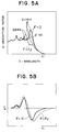
- Fig. 5A is a representation illustrating the relationship between an absorption factor of a quantum well layer and an electric field applied thereto for explaining the basic principle of the present invention.
- Fig. 5B is a representation illustrating the relationship between a refractive index variation ⁇ n of the quantum well layer and the electric field for explaining the basic principle of the present invention.
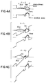
- Fig. 6A is a cross-sectional view of a first embodiment of the present invention.
- Fig. 6B is a representation illustrating the energy band struture of a quantum well layer of the first embodiment.
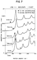
- Fig. 7 is a representation illustrating the electric field dependency of an absorption factor of the first embodiment.
- Figs. 8A-8D are respectively representations illustrating the electric field dependency of a refractive index variance ⁇ n of the first embodiment.
- Fig. 9 is a cross-sectional view of a second embodiment of the present invention.
- Fig 10 is a representation illustrating a transmission factor spectrum of the second embodiment.
- Fig. 11 is a cross-sectional view of a third embodiment of the present invention.
- Fig. 12 is a representation illustrating the wavelength dependency of an intensity of emitting light of the third embodiment.
- Fig. 13 is a block diagram showing an example of optical communication systems in which the optical device of the present invention is used as a filter and a light modulating device.
- the basic principle of the present invention will be explained by use of an example in which the ADQW consisting of two different quantum wells 1 and 2 (shallow well 1 of a wide width and deep well 2 of a narrow width) coupled to each other has an energy band structure as shown in Fig. 4A.
- the wave functions ⁇ E1 and ⁇ E2 vary as shown in Figs. 4B and 4C.
- the wave function ⁇ E1 which is confined in the deep well 2 when no electric field is applied (Fig. 4A) begins to spread toward the wide, shallow well 1 as the applied electric field increases.
- the wave function ⁇ E2 comes to have a dense part in the narrow, deep well 2 as the applied electric field increases.
- the wave function ⁇ HH1 of holes scarcely varies even if the electric field increases.
- the absorption factor ⁇ ex of an exciton is proportional to an overlap integral between wave functions of electrons and holes as represented by: ⁇ ex ⁇ ⁇ ⁇ E ⁇ ⁇ H dz (1) Therefore, as is seen from Figs. 4B and 4C, the absorption ⁇ ex abruptly decreases as the electric field increases because the overlap between the wave functions ⁇ E and ⁇ H abruptly decreases as the electric field is increased.
- the energy or photon energy of exciton scarcely varies since the width of the deep well 2 is narrow and an energy gap between the levels E1 and HH1 scarcely varies. Namely, the intensity of an exciton peak due to transition between the lowest energy level E1 and the energy level of heavy hole HH1 abruptly decreases as the electric field decreases. And the amount of a red shift of exciton peak in which the energy or photon energy shifts to a lower value is small, differently from normal QCSE.
- Fig 5A illustrates the above-discussed situation.
- the wavelength or photon energy dependency of the absorption factor ⁇ varies in the following manner as the electric field is increased from zero to F1 and F2.
- the electric field is F1
- the exciton peak of transition between the levels E2 and HH1 begins to appear and the exciton peak of transition between the levels E1 and HH1 abruptly decreases as indicated by dotted lines.
- the electric field is F2
- the exciton peak between the levels E1 and HH1 almost disappears as indicated by dash and dotted lines.
- the energy (wavelength or photon energy) of the exciton peak between the levels E1 and HH1 remains almost unchanged as shown in Fig. 5A.
- the spectrum of the refractive index variance ⁇ n at this time is shown in Fig. 5B.
- the absorption factor ⁇ remains almost unchanged since the red shift of the exciton peak between the levels E1 and HH1 scarcely occurs and only its intensity decreases as is explained referring to Fig. 5A.
- the refractive index is considerably changed for the light of wavelength ⁇ 1 as shown in Fig. 5B.
- Fig. 6A shows a first embodiment of a phase modulator which uses the above-discussed principle and in which the amplitude of modulation is large and the variation of output intensity is small.
- Fig. 6B illustrates the energy band structure of its quantum well layer structure.
- an electrode 34 for applying an electric field to the ADQW layer 33 is formed on the bottom surface of the substrate 31, another electrode 34' for applying the electric field to the ADQW layer 33 is formed.
- Anti-reflection coats 35 and 35' are respectively deposited on both end surfaces of the wafer for eliminating reflections at light input and output end surfaces.
- the ADQW layer 33 is comprised of, from the side of tile substrate 31, an i-Al 0.16 Ga 0.84 As 41 well layer having a thickness of 80 ⁇ , an i-GaAs well layer 42 having a thickness of 40 ⁇ and an i-Al 0.4 Ga 0.6 As barrier layer 43 having a thickness of 20 ⁇ and formed therebetween as shown in Fig. 6B in the form of an energy band structure. Further, two i-Al 0.5 Ga 0.5 As barrier layers 44 and 44' having a thickness of 100 ⁇ are respectively formed outside of the well layers 41 and 42 to build the ADQW structure. In Fig. 6B, the right side corresponds to an upper side of the wafer of Fig. 6A.
- the wavelength dependencies of the absorption factor ⁇ of the quantum well layer 33 in the first embodiment are represented in Fig. 7.
- the absorption factor ⁇ is in the vicinity of zero for photon energy of 1.50 eV.
- the exciton peak (indicated by black triangles) of the transition between the levels E1 and HH1 disappears at the electric field 75 kV/cm, and instead the exciton peak [indicated by white triangles) of the transition between the levels E2 and HH1 appears.
- the photon energy of the exciton peak of the transition between the levels E1 and HH1 remains almost unchanged until the electric field of 50kV/cm.
- the absorption factor ⁇ for photon energies below 1.55 eV remains almost unchanged irrespective of the change in electric field.
- Figs. 8A-8D illustrate the wavelength dependencies of the refractive index variation ⁇ n due to the electric field for respective applied electric fields. It is seen therefrom that the refractive index variation ⁇ n of about 5 ⁇ 10 ⁇ 3 is obtained even for photon energies below 1.53 eV at which the absorption factor ⁇ is small.
- the length of the waveguide shown in Fig. 6A is set to 200 ⁇ m.
- photon energy: 1.52 eV photon energy: 1.52 eV
- Fig. 9 shows a second embodiment of a tunable filter which uses the above-discussed principle.
- an n-GaAs substrate 61 on an n-GaAs substrate 61, an n-Al 0.5 Ga 0.5 As clad layer 62 having a thickness of 1.5 ⁇ m, an ADQW layer 63.
- a p-Al 0.5 Ga 0.5 As clad layer 62' having a thickness of 1.5 ⁇ m and an electrode 64 for applying an electric field to the ADQW layer 63.
- another electrode 64' For applying the electric field to the ADQW layer 63 is formed.
- Anti-reflection coats 65 and 65' are respectively deposited on both ends of the wafer for eliminating reflections at light input and output end surfaces.
- These layers and coats 61-65 and 65' are the same as those 31-35 and 35' of the first embodiment shown in Fig. 6A in material and structure.
- a grating 67 is formed on the light guide layer 66' , and a portion 68 for shifting its phase by ⁇ /2 is formed on the grating 67 for stabilizing a wavelength to be selected or filtered.
- a transmission spectrum as illustrated in Fig. 10 is obtained.
- a pitch of the grating 67 is ⁇
- the application of an electric field of 50 eV/cm sufficed for shifting the Bragg diffraction wavelength ⁇ B by 12 ⁇ and the variance of an intensity of an output light fell within 1 dB.
- a tunable filter which is capable of obtaining a filtering wavelength shift of 12 ⁇ with a stable output is achieved.
- Fig. 11 shows a third embodiment which can solve the drawback of the second embodiment.
- the third embodiment uses the filter of the second embodiment as a reflector part and further includes an amplifying part with an active layer 83' .
- a filter with an amplification function is obtained and the third embodiment is capable of amplifying light of the Bragg wavelength ⁇ B and emitting the same.
- reference numerals 81-88 denote the same layers and portions 61-68 of the second embodiment of Fig. 9.
- the i-Al 0.1 Ga 0.9 As active layer 83' having a thickness of 0.1 ⁇ m, an electrode 90 for injecting current therethrough and a groove 89 for dividing elctrodes 84 and 90 from each other.
- a phase modulating device with a great modulation and a stable output is attained since there is provided a semionductor quantum well layer in which the shift of an exciton peak wavelength due to QCSE by the application of a reverse bias electric field almost disappears and only a refractive index is changed in a given range of wavelength by the application of the electric field while an absorption factor is very small and remains unchanged in such wavelength range.
- a tunable filter with a wide width of tunable wavelength and a stable output is attained. Consequently, an electric field modulation type optical device with little output variation is achieved since the variation of absorption factor due to the application of electric field is small.
- Fig. 13 shows a block diagram illustrating an optical communication system in which the devices of the present invention can be used as a light modulator or a filter.
- reference numeral 186 is an optical fiber for transmitting light signals.
- a plurality of terminals 1881, 1882, ⁇ ⁇ ⁇ , 188 n are connected to the optical fiber 186 through optical nodes 1871, 1872, ⁇ ⁇ ⁇ , , 187 n , respectively.
- Terminal units 1891, 1892, ⁇ ⁇ ⁇ , 189 n are connected to the respective terminals.
- Each terminal unit includes a keyboard, a display device, etc.
- each terminal there are provided a light signal transmitter consisting of a light modulator 182 and a modulator driver 183 and a light signal receiver consisting of a filter 179, a photodetector 180 and a demodulator 181.
- the transmitter and receiver are controlled by a controller 184 according to instructions from the terminal unit 1891.
- the light modulator 182 modulates a constant light from a laser diode (not shown) according to a signal from the driver 183. Namely, an external modulation is conducted instead a direct modulation.
- the filter 179 selects a signal of desired wavelength from plural signals of different wavelengths and outputs this desired signal to the photodetector 180 (in this case, the wavelength division multiplexing is conducted).
- An optical device includes an asymmetric dual quantum well (ADQW) structure which is comprised of a plur ality(at least two) of different semiconductor quantum well layers coupled to each other.
- ADQW asymmetric dual quantum well
- the width of a deeper quantum well layer having a narrower band gap is made narrower than that of a less deeper quantum well layer having a wider band gap such that the shift of an exciton wavelength is scarcely caused due to the quantum confined Stark effect by the application of an electric field in a predetermined range.
- a refractive index of the ADQW structure is changed, but an absorption factor is scarcely changed for a given range of wavelength by the application of the electric field.
- a member for applying an electric field to the asymmetric dual quantum well structure is provided.
Landscapes
- Physics & Mathematics (AREA)
- Optics & Photonics (AREA)
- General Physics & Mathematics (AREA)
- Nanotechnology (AREA)
- Nonlinear Science (AREA)
- Electromagnetism (AREA)
- Condensed Matter Physics & Semiconductors (AREA)
- Chemical & Material Sciences (AREA)
- Engineering & Computer Science (AREA)
- Crystallography & Structural Chemistry (AREA)
- Biophysics (AREA)
- Life Sciences & Earth Sciences (AREA)
- Semiconductor Lasers (AREA)
- Optical Integrated Circuits (AREA)
- Photo Coupler, Interrupter, Optical-To-Optical Conversion Devices (AREA)
- Optical Modulation, Optical Deflection, Nonlinear Optics, Optical Demodulation, Optical Logic Elements (AREA)
Applications Claiming Priority (2)
| Application Number | Priority Date | Filing Date | Title |
|---|---|---|---|
| JP2289644A JPH04163967A (ja) | 1990-10-27 | 1990-10-27 | 光デバイス |
| JP289644/90 | 1990-10-27 |
Publications (3)
| Publication Number | Publication Date |
|---|---|
| EP0483687A2 true EP0483687A2 (de) | 1992-05-06 |
| EP0483687A3 EP0483687A3 (en) | 1992-10-28 |
| EP0483687B1 EP0483687B1 (de) | 1997-07-23 |
Family
ID=17745910
Family Applications (1)
| Application Number | Title | Priority Date | Filing Date |
|---|---|---|---|
| EP91118250A Expired - Lifetime EP0483687B1 (de) | 1990-10-27 | 1991-10-25 | Optische Vorrichtung mit asymmetrischer Doppel-Quantumwell-Struktur |
Country Status (5)
| Country | Link |
|---|---|
| US (1) | US5569934A (de) |
| EP (1) | EP0483687B1 (de) |
| JP (1) | JPH04163967A (de) |
| AT (1) | ATE155900T1 (de) |
| DE (1) | DE69126942T2 (de) |
Cited By (6)
| Publication number | Priority date | Publication date | Assignee | Title |
|---|---|---|---|---|
| EP0554178A1 (de) * | 1992-01-31 | 1993-08-04 | France Telecom | Optischer Halbleiterverstärker mit kurzer Schaltzeit |
| EP0622654A3 (de) * | 1993-04-24 | 1994-12-21 | Sel Alcatel Ag | Optoelektronisches Halbleiterbauelement. |
| GB2279499A (en) * | 1993-06-25 | 1995-01-04 | Mitsubishi Electric Corp | Semiconductor optical modulator |
| GB2307304A (en) * | 1995-11-16 | 1997-05-21 | Toshiba Cambridge Res Center | Optical semiconductor device |
| WO2004042881A3 (en) * | 2002-11-08 | 2004-12-16 | Univ London | Optical frequency comb generator |
| US7522645B2 (en) | 2006-09-20 | 2009-04-21 | Kabushiki Kaisha Toshiba | Nitride-based semiconductor laser device |
Families Citing this family (24)
| Publication number | Priority date | Publication date | Assignee | Title |
|---|---|---|---|---|
| JP3921268B2 (ja) * | 1997-03-19 | 2007-05-30 | 富士通株式会社 | 半導体光変調器 |
| GB9912583D0 (en) * | 1999-05-28 | 1999-07-28 | Arima Optoelectronics Corp | A light emitting diode having a two well system with asymmetric tunneling |
| WO2001033287A1 (en) * | 1999-10-28 | 2001-05-10 | Center For Advanced Science And Technology Incubation, Ltd. | Electroabsorption optical modulator and method for fabricating the same |
| US7072534B2 (en) * | 2002-07-22 | 2006-07-04 | Applied Materials, Inc. | Optical ready substrates |
| US7110629B2 (en) * | 2002-07-22 | 2006-09-19 | Applied Materials, Inc. | Optical ready substrates |
| US7043106B2 (en) * | 2002-07-22 | 2006-05-09 | Applied Materials, Inc. | Optical ready wafers |
| WO2005001520A2 (en) * | 2003-05-29 | 2005-01-06 | Applied Materials, Inc. | Serial routing of optical signals |
| EP1649566A4 (de) * | 2003-06-27 | 2007-08-15 | Applied Materials Inc | Gepulstes quanten-dot-lasersystem mit niedrigem jitter |
| US20050016446A1 (en) | 2003-07-23 | 2005-01-27 | Abbott John S. | CaF2 lenses with reduced birefringence |
| FI20041213A0 (fi) * | 2004-09-17 | 2004-09-17 | Optogan Oy | Puolijohdeheterorakenne |
| US20060222024A1 (en) * | 2005-03-15 | 2006-10-05 | Gray Allen L | Mode-locked semiconductor lasers with quantum-confined active region |
| US20060227825A1 (en) * | 2005-04-07 | 2006-10-12 | Nl-Nanosemiconductor Gmbh | Mode-locked quantum dot laser with controllable gain properties by multiple stacking |
| WO2007027615A1 (en) * | 2005-09-01 | 2007-03-08 | Applied Materials, Inc. | Ridge technique for fabricating an optical detector and an optical waveguide |
| WO2007065614A2 (en) * | 2005-12-07 | 2007-06-14 | Innolume Gmbh | Laser source with broadband spectrum emission |
| US7835408B2 (en) * | 2005-12-07 | 2010-11-16 | Innolume Gmbh | Optical transmission system |
| US7561607B2 (en) * | 2005-12-07 | 2009-07-14 | Innolume Gmbh | Laser source with broadband spectrum emission |
| US8707559B1 (en) | 2007-02-20 | 2014-04-29 | Dl Technology, Llc | Material dispense tips and methods for manufacturing the same |
| WO2010065731A2 (en) * | 2008-12-03 | 2010-06-10 | Innolume Gmbh | Semiconductor laser with low relative intensity noise of individual longitudinal modes and optical transmission system incorporating the laser |
| US8864055B2 (en) | 2009-05-01 | 2014-10-21 | Dl Technology, Llc | Material dispense tips and methods for forming the same |
| US9725225B1 (en) | 2012-02-24 | 2017-08-08 | Dl Technology, Llc | Micro-volume dispense pump systems and methods |
| KR101902928B1 (ko) | 2013-01-04 | 2018-10-02 | 삼성전자주식회사 | 3중 연결 양자우물 구조를 포함하는 광학 소자 |
| KR102113256B1 (ko) | 2013-11-07 | 2020-05-20 | 삼성전자주식회사 | 다준위 에너지를 갖는 3중 연결 양자우물 구조를 포함하는 광학 소자 |
| KR102213661B1 (ko) | 2014-04-04 | 2021-02-08 | 삼성전자주식회사 | 3중 연결 양자우물 구조를 포함하는 광학 소자 |
| US11746656B1 (en) | 2019-05-13 | 2023-09-05 | DL Technology, LLC. | Micro-volume dispense pump systems and methods |
Family Cites Families (10)
| Publication number | Priority date | Publication date | Assignee | Title |
|---|---|---|---|---|
| US4122407A (en) * | 1976-04-06 | 1978-10-24 | International Business Machines Corporation | Heterostructure junction light emitting or responding or modulating devices |
| US4727341A (en) * | 1985-06-28 | 1988-02-23 | Nec Corporation | Optical modulator |
| JPH01204019A (ja) * | 1988-02-10 | 1989-08-16 | Nec Corp | 光変調器 |
| JP2686764B2 (ja) * | 1988-03-11 | 1997-12-08 | 国際電信電話株式会社 | 光半導体素子の製造方法 |
| US4884119A (en) * | 1988-04-22 | 1989-11-28 | American Telephone & Telegraph Company | Integrated multiple quantum well photonic and electronic devices |
| FR2637092B1 (fr) * | 1988-05-11 | 1991-04-12 | Thomson Csf | Modulateur d'onde electromagnetique a puits quantiques couples, et application a un detecteur d'onde electromagnetique |
| JP2719189B2 (ja) * | 1988-09-09 | 1998-02-25 | 富士通株式会社 | 光半導体装置 |
| JPH02164111A (ja) * | 1988-12-17 | 1990-06-25 | Sumitomo Electric Ind Ltd | 半導体装置 |
| JP2864462B2 (ja) * | 1989-12-08 | 1999-03-03 | キヤノン株式会社 | 半導体光素子及びその使用方法 |
| US5103455A (en) * | 1990-05-09 | 1992-04-07 | Gte Laboratories Incorporated | Monolithically integrated semiconductor optical preamplifier |
-
1990
- 1990-10-27 JP JP2289644A patent/JPH04163967A/ja active Pending
-
1991
- 1991-10-25 DE DE69126942T patent/DE69126942T2/de not_active Expired - Fee Related
- 1991-10-25 AT AT91118250T patent/ATE155900T1/de not_active IP Right Cessation
- 1991-10-25 EP EP91118250A patent/EP0483687B1/de not_active Expired - Lifetime
-
1995
- 1995-09-28 US US08/535,349 patent/US5569934A/en not_active Expired - Fee Related
Cited By (10)
| Publication number | Priority date | Publication date | Assignee | Title |
|---|---|---|---|---|
| EP0554178A1 (de) * | 1992-01-31 | 1993-08-04 | France Telecom | Optischer Halbleiterverstärker mit kurzer Schaltzeit |
| EP0622654A3 (de) * | 1993-04-24 | 1994-12-21 | Sel Alcatel Ag | Optoelektronisches Halbleiterbauelement. |
| US5550670A (en) * | 1993-04-24 | 1996-08-27 | Alcatel N.V. | Electro-optic modulator using multiple quantum well structure having stark-effect quantum Barriers and non-stark-effect quantum barriers sandwiched therebetween |
| GB2279499A (en) * | 1993-06-25 | 1995-01-04 | Mitsubishi Electric Corp | Semiconductor optical modulator |
| US5521742A (en) * | 1993-06-25 | 1996-05-28 | Mitsubishi Denki Kabushiki Kaisha | Semiconductor optical modulator |
| GB2279499B (en) * | 1993-06-25 | 1997-03-26 | Mitsubishi Electric Corp | Semiconductor optical modulator |
| GB2307304A (en) * | 1995-11-16 | 1997-05-21 | Toshiba Cambridge Res Center | Optical semiconductor device |
| GB2307304B (en) * | 1995-11-16 | 2000-04-05 | Toshiba Cambridge Res Center | Optical device |
| WO2004042881A3 (en) * | 2002-11-08 | 2004-12-16 | Univ London | Optical frequency comb generator |
| US7522645B2 (en) | 2006-09-20 | 2009-04-21 | Kabushiki Kaisha Toshiba | Nitride-based semiconductor laser device |
Also Published As
| Publication number | Publication date |
|---|---|
| EP0483687A3 (en) | 1992-10-28 |
| US5569934A (en) | 1996-10-29 |
| JPH04163967A (ja) | 1992-06-09 |
| DE69126942D1 (de) | 1997-09-04 |
| DE69126942T2 (de) | 1998-02-05 |
| ATE155900T1 (de) | 1997-08-15 |
| EP0483687B1 (de) | 1997-07-23 |
Similar Documents
| Publication | Publication Date | Title |
|---|---|---|
| EP0483687B1 (de) | Optische Vorrichtung mit asymmetrischer Doppel-Quantumwell-Struktur | |
| US5801872A (en) | Semiconductor optical modulation device | |
| US5208822A (en) | Semiconductor element having opposite signs of α parameter | |
| KR0147835B1 (ko) | 광장치 | |
| US5339370A (en) | Optical modulator and optical communication system utilizing the same | |
| US5757832A (en) | Optical semiconductor device, driving method therefor and light source and opitcal communication system using the same | |
| JPH07307530A (ja) | 偏波変調可能な半導体レーザ | |
| Lee et al. | Wavelength-tunable and single-frequency semiconductor lasers for photonic communications networks | |
| US5495360A (en) | 1.5 μm wavelength asymmetric fabry-perot modulator with negative chirp | |
| Oshiba et al. | Low-drive-voltage MQW electroabsorption modulator for optical short-pulse generation | |
| JPH0732279B2 (ja) | 半導体発光素子 | |
| US6825505B2 (en) | Phase-shifted distributed feedback type semiconductor laser diode capable of improving wavelength chirping and external reflection return light characteristics | |
| EP0296066B1 (de) | Integrierte Laservorrichtung mit Brechungsindex-Modulator | |
| KR100500097B1 (ko) | 광변조기 | |
| EP0444607B1 (de) | Optisches Wellenleiterelement und Verfahren zum Betreiben desselben | |
| US6785312B2 (en) | Semiconductor laser and system for and method of performing digital optical communications using such semiconductor laser | |
| JPH07231132A (ja) | 半導体光装置 | |
| JP2001013472A (ja) | 光半導体素子および光通信装置 | |
| US5999298A (en) | Electroabsorption optical intesity modulator having a plurality of absorption edge wavelengths | |
| US5973339A (en) | Semiconductor photodetector having an optical attenuator | |
| US6356382B1 (en) | Optical wavelength converter with active waveguide | |
| EP0551863A1 (de) | Optisches Halbleiterfilter und dessen Verwendung in einem optischen Kommunikationssystem | |
| US6332048B1 (en) | Modulator and method for manufacturing of such a modulator | |
| US20040001243A1 (en) | Semiconductor optical modulator and semiconductor optical device | |
| US5920419A (en) | Quantum well electro-optical modulator |
Legal Events
| Date | Code | Title | Description |
|---|---|---|---|
| PUAI | Public reference made under article 153(3) epc to a published international application that has entered the european phase |
Free format text: ORIGINAL CODE: 0009012 |
|
| AK | Designated contracting states |
Kind code of ref document: A2 Designated state(s): AT BE CH DE DK ES FR GB GR IT LI LU NL SE |
|
| PUAL | Search report despatched |
Free format text: ORIGINAL CODE: 0009013 |
|
| AK | Designated contracting states |
Kind code of ref document: A3 Designated state(s): AT BE CH DE DK ES FR GB GR IT LI LU NL SE |
|
| 17P | Request for examination filed |
Effective date: 19930315 |
|
| 17Q | First examination report despatched |
Effective date: 19941223 |
|
| GRAG | Despatch of communication of intention to grant |
Free format text: ORIGINAL CODE: EPIDOS AGRA |
|
| GRAH | Despatch of communication of intention to grant a patent |
Free format text: ORIGINAL CODE: EPIDOS IGRA |
|
| GRAH | Despatch of communication of intention to grant a patent |
Free format text: ORIGINAL CODE: EPIDOS IGRA |
|
| GRAA | (expected) grant |
Free format text: ORIGINAL CODE: 0009210 |
|
| AK | Designated contracting states |
Kind code of ref document: B1 Designated state(s): AT BE CH DE DK ES FR GB GR IT LI LU NL SE |
|
| PG25 | Lapsed in a contracting state [announced via postgrant information from national office to epo] |
Ref country code: IT Free format text: LAPSE BECAUSE OF FAILURE TO SUBMIT A TRANSLATION OF THE DESCRIPTION OR TO PAY THE FEE WITHIN THE PRESCRIBED TIME-LIMIT;WARNING: LAPSES OF ITALIAN PATENTS WITH EFFECTIVE DATE BEFORE 2007 MAY HAVE OCCURRED AT ANY TIME BEFORE 2007. THE CORRECT EFFECTIVE DATE MAY BE DIFFERENT FROM THE ONE RECORDED. Effective date: 19970723 Ref country code: NL Free format text: LAPSE BECAUSE OF FAILURE TO SUBMIT A TRANSLATION OF THE DESCRIPTION OR TO PAY THE FEE WITHIN THE PRESCRIBED TIME-LIMIT Effective date: 19970723 Ref country code: BE Effective date: 19970723 Ref country code: GR Free format text: LAPSE BECAUSE OF FAILURE TO SUBMIT A TRANSLATION OF THE DESCRIPTION OR TO PAY THE FEE WITHIN THE PRESCRIBED TIME-LIMIT Effective date: 19970723 Ref country code: ES Free format text: THE PATENT HAS BEEN ANNULLED BY A DECISION OF A NATIONAL AUTHORITY Effective date: 19970723 Ref country code: CH Effective date: 19970723 Ref country code: DK Effective date: 19970723 Ref country code: LI Effective date: 19970723 Ref country code: AT Effective date: 19970723 |
|
| REF | Corresponds to: |
Ref document number: 155900 Country of ref document: AT Date of ref document: 19970815 Kind code of ref document: T |
|
| REG | Reference to a national code |
Ref country code: CH Ref legal event code: EP |
|
| REF | Corresponds to: |
Ref document number: 69126942 Country of ref document: DE Date of ref document: 19970904 |
|
| ET | Fr: translation filed | ||
| PG25 | Lapsed in a contracting state [announced via postgrant information from national office to epo] |
Ref country code: SE Effective date: 19971023 |
|
| PG25 | Lapsed in a contracting state [announced via postgrant information from national office to epo] |
Ref country code: LU Free format text: LAPSE BECAUSE OF NON-PAYMENT OF DUE FEES Effective date: 19971031 |
|
| NLV1 | Nl: lapsed or annulled due to failure to fulfill the requirements of art. 29p and 29m of the patents act | ||
| REG | Reference to a national code |
Ref country code: CH Ref legal event code: PL |
|
| PLBE | No opposition filed within time limit |
Free format text: ORIGINAL CODE: 0009261 |
|
| STAA | Information on the status of an ep patent application or granted ep patent |
Free format text: STATUS: NO OPPOSITION FILED WITHIN TIME LIMIT |
|
| 26N | No opposition filed | ||
| REG | Reference to a national code |
Ref country code: GB Ref legal event code: IF02 |
|
| PGFP | Annual fee paid to national office [announced via postgrant information from national office to epo] |
Ref country code: FR Payment date: 20031003 Year of fee payment: 13 |
|
| PGFP | Annual fee paid to national office [announced via postgrant information from national office to epo] |
Ref country code: GB Payment date: 20031022 Year of fee payment: 13 |
|
| PGFP | Annual fee paid to national office [announced via postgrant information from national office to epo] |
Ref country code: DE Payment date: 20031103 Year of fee payment: 13 |
|
| PG25 | Lapsed in a contracting state [announced via postgrant information from national office to epo] |
Ref country code: GB Free format text: LAPSE BECAUSE OF NON-PAYMENT OF DUE FEES Effective date: 20041025 |
|
| PG25 | Lapsed in a contracting state [announced via postgrant information from national office to epo] |
Ref country code: DE Free format text: LAPSE BECAUSE OF NON-PAYMENT OF DUE FEES Effective date: 20050503 |
|
| GBPC | Gb: european patent ceased through non-payment of renewal fee |
Effective date: 20041025 |
|
| PG25 | Lapsed in a contracting state [announced via postgrant information from national office to epo] |
Ref country code: FR Free format text: LAPSE BECAUSE OF NON-PAYMENT OF DUE FEES Effective date: 20050630 |
|
| REG | Reference to a national code |
Ref country code: FR Ref legal event code: ST |