EP0483829A2 - Circuit de contrôle pour afficheur - Google Patents
Circuit de contrôle pour afficheur Download PDFInfo
- Publication number
- EP0483829A2 EP0483829A2 EP91118565A EP91118565A EP0483829A2 EP 0483829 A2 EP0483829 A2 EP 0483829A2 EP 91118565 A EP91118565 A EP 91118565A EP 91118565 A EP91118565 A EP 91118565A EP 0483829 A2 EP0483829 A2 EP 0483829A2
- Authority
- EP
- European Patent Office
- Prior art keywords
- led
- indicator
- control circuit
- switches
- circuit according
- Prior art date
- Legal status (The legal status is an assumption and is not a legal conclusion. Google has not performed a legal analysis and makes no representation as to the accuracy of the status listed.)
- Withdrawn
Links
Images





Classifications
-
- G—PHYSICS
- G09—EDUCATION; CRYPTOGRAPHY; DISPLAY; ADVERTISING; SEALS
- G09G—ARRANGEMENTS OR CIRCUITS FOR CONTROL OF INDICATING DEVICES USING STATIC MEANS TO PRESENT VARIABLE INFORMATION
- G09G3/00—Control arrangements or circuits, of interest only in connection with visual indicators other than cathode-ray tubes
- G09G3/001—Control arrangements or circuits, of interest only in connection with visual indicators other than cathode-ray tubes using specific devices not provided for in groups G09G3/02 - G09G3/36, e.g. using an intermediate record carrier such as a film slide; Projection systems; Display of non-alphanumerical information, solely or in combination with alphanumerical information, e.g. digital display on projected diapositive as background
Definitions
- the present invention relates to a control circuit for an operating panel or operation console and the like, and more particularly to one preferably used in a circuit for controlling a turn-on operation of a display or indicatior device such as LED (Light Emitting Diode) provided on an operating or indicator panel in a printing apparatus and the like.
- a display or indicatior device such as LED (Light Emitting Diode) provided on an operating or indicator panel in a printing apparatus and the like.
- an operating panel in a printing apparatus and the like is provided with a control circuit having a display or indicator unit for informing an operator of an operational state of the function and operating switches, which are controlled by a control unit.
- FIG. 9 is an elevational view of a conventional operating panel by way of example.
- a plurality of light emitting diodes designated by LED1 - LED16 as display means and a plurality of operating or control switches designated by SW1 - SW8.
- Those elements LED1 - LED16 and SW1 - SW8 are disposed on a printed circuit board 2 and attached to the back surface of an operating panel 1.
- light emitting diodes LED1 - LED16 serve to indicate, when lighting, functions which are now in turn-on state.
- FIG. 10 is a diagram of a conventional control circuit by way of example.
- a control circuit 3 comprises driver electronics 4 for driving LED1 - LED16, current control resistors R1 - R16 each for determining luminance of the associated light emitting diode, switches SW1 - SW8 and pull-up resistors R17 - R24.
- the control circuit 3 is controlled by a central processor unit (CPU) 5.
- the driver 4 is provided with output terminals O1 - O16 each connected in series to associated one of the elements LED1 - LED16 to which the resistors R1 - R16 are connected in series, respectively.
- the resistors R1 - R16 are put to the ground at the other ends thereof by a common connection.
- Input terminals I1 - I16 of the driver 4 are connected through terminals T1 - T16 provided on a printed circuit board 2 to ports P1 - P16 of CPU 5, respectively.
- ports P17 - P24 of CPU 5 are connected through terminals T17 - T24 to one terminals of SW1 - SW8, respectively.
- the SW1 - SW8 are put to the ground at the other ends thereof.
- the one terminals of the SW1 - SW8 are connected to associated one terminals of the pull-up resistors R17 - R24, respectively, which are grounded at the other terminals thereof.
- Central processor unit 5 outputs a signal of level "1" through ports P1 - P16 to a light emitting diode corresponding to function which is now in turn-on state, so that the driver 4 is driven to light that light emitting diode.
- ports P17 - P24 of CPU 5 are detected to determine depression of swithces SW1 - SW8 by discriminating whether or not the port corresponding to the depressed switch is now in level "0".
- the conventional control circuit has been associated with the following drawbacks. There are required wirings for connection of the switches SW1 - SW8 and the associated ports. Thus, the number of wirings for connection is increased, thereby enlarging the required area of the printed circuit board.
- the number of terminals in the terminal unit of the printed circuit board needs the sum of the number of LED's and the number of operating switches.
- the number of circuit connection patterns provided on the printed circuit board also requires the associated number of terminals, thereby enlarging the area of the printed circuit board.
- an indicator control circuit for controlling a drive operation of a lighting indicator unit provided with a plurality of indicator elements each adapted to indicate an operating condition of an electronic apparatus.
- the indicator control circuit comprises an indicator element driver unit provided with ports the number of which corresponds to that of the plurality of indicator elements, each of the ports being connected by a signal line to associated one of the plurality of indicator elements to supply a driving signal to the associated indicator element; an operating switch unit comprising a plurality of operating switches each of which is connected to associated one of the ports of the indicator element driver unit through associated one of the signal lines for connecting the ports and the indicator elements on a common basis; a switch condition detector for providing such a control that while the indicator element driver unit drives the indicator elements, the driving operation is stopped for a moment and at that time potential of each of the ports of the indicator element driver unit, to which the switches are connected, is sensed, so that turn-on/turn-off states of the switches are detected and turn-on/turn-off information representative of the turn-on/turn-off states
- the present invention provides a control circuit having a plurality of indicator elements and a plurality of switches, for lighting the indicator elements and sensing switching conditions of the switches on the basis of a control signal transmitted from a control unit.
- the control circuit is provided with a serial-to-parallel converter having input terminals and output terminals for converting a serial signal transmitted from the control unit into a parallel signal.
- the output terminals of the serial-to-parallel converter are connected with the plurality of indicator elements, which are put to a reference potential at other ends thereof, and some output terminals of the serial-to-parallel converter are further connected with the plurality of switches, to which a switch condition sensor is connected at other ends thereof on a common basis, while the switch condition sensor is put to the reference potential at another end thereof.
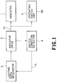
- FIG. 1 is a diagram schematically showing a functional structure of an indicator control circuit according to an embodiment of the present invention.
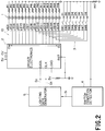
- FIG. 2 is a diagram useful for understanding a wiring state of the indicator control circuit according to the embodiment of the present invention.
- the indicator or display control circuit basically comprises an indicator unit 1, an indicator driver circuit or electronics 2, an operating or control switch unit 3, a switch condition detector 4 and a lighting data generator 5. It is noted that actually the switch condition detector 4 and the lighting data generator 5 are constructed into program sequences stored in a central processor system, which will be described later.
- the indicator or display unit 1 is provided for indicating an operating condition of an electronic apparatus and the like such as a printer.
- As indicator or display devices for informing the operating conditions of the apparatus there are disposed a plurality of light emitting diodes LED 1 - LED 16.
- the light emitting diodes LED 1 - LED 16 are driven by the indicator driver circuit 2.
- the indicator driver circuit 2 is provided with ports O16 - O1 the number of which corresponds to that of the light emitting diodes LED 1 - LED 16.
- Each of the ports O16 - O1 is connected by a signal line 10 to associated one of the light emitting diodes LED 1- LED 16 to supply a driving signal to the associated LED.
- the signal lines 10 for connecting the ports O16 - O1 and diodes LED 1 - LED 16 are used on a common basis in such a manner that a plurality of operating switches SW 1 - SW 8 are connected to the ports O1 - O8 of the indicator lamp driver circuit 2, respectively.
- the operating switches SW 1 - SW 8 are provided on the operating or control switch unit 3 to produce associated command signals for controlling operation of the apparatus.
- the switches SW 1 - SW 8 are put to the ground as a reference potential through diodes D 1 - D 8 at the other terminals thereof. Consequently, if any of the switches SW 1 - SW 8 is closed or turned on, the port O, to which the closed switch SW is connected, goes down in its potential to low level "L".
- sensing of the potential of the port O makes it possible to detect turn-on/turn-off states of the switches SW 1 - SW 8.
- the diodes D 1 - D 8 are provided for the purpose of protection of driver electronics, advantageously implemented in a single integrated circuit chip, constructing the indicator driver circuit 2 from short-circuiting in its output in case of simultaneous depression of plural switches SW's.
- the switch condition detector 4 provides such a control that while the indicator driver circuit 2 drives light emitting diode LED 1 - LED 16 to light, the driving operation is ceased for a moment, and at that time potential on each of the ports of the indicator driver circuit 2 to which the switches SW1 - SW 8 are connected is sensed, so that turn-on/turn-off states of the switches SW 1 - SW 8 are detected and a switch condition detection signal S1 is outputted to indicate the sensed condition.
- the lighting data generator 5 generates data for lighting operation of the respective LED 1 - LED 16 on the basis of the given information.
- the indicator driver circuit 2 or the driver electronics 2, is provided with a means for converting a serial input to a parallel output, which has 16 bits of parallel output, in accordance with the present embodiment. Between the respective LED 1 - LED 16 and the ground, there are provided current control resistors R1- R16 each for determining luminance of associated one of the light emitting diodes LED 1 - LED 16.
- an input portion of the driver electronics 2 is provided with a serial data input terminal DATA and a serial clock input terminal CLK, to which a serial data signal S2 and a serial clock signal S3 are applied from the lighting data generator 5, respectively.
- FIG. 3 is a time chart useful for understanding a method of lighting the light emitting diodes.
- the lighting data generator 5 sends the serial data signal S2 (hexadicimal data (B153)H, for example) in synchronism with the serial clock signal S3. The data is changed at the leading edge of the serial clock signal.
- the serial data signal S2 is shifted through a shift register, not shown and provided within the driver IC 2, and has been set to the ports O1 - O16 after the serial clock signal S3 is terminated, so that the light emitting diode or diodes corresponding to the conditions of the serial data signal S2 are driven to light.
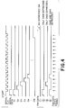
- FIG. 4 is a time chart used for describing how the switches SW 1-SW 8 are sensed.
- the lighting data generator 5 sends data (8000)H in synchronism with the serial clock signal S3, the data being changed at the leading edge of the serial clock signal.
- the data to be latched is changed in response to a depressed condition of the switch, for example, changed to (0000)H if none of the switches is depressed, and (8000)H if the switch SW 8 is depressed.
- signals SW - DATA are latched in synchronism with the serial clock signal S3 at the trailing edge of the serial clock signal.
- the signal SW - DATA becomes "1", only at a timing wherein a switch is depressed and a port of the driver electronics 2 outputs "1".
- encircled numeral 1 designates a state of the signal SW - DATA in a case where none of the switches SW 1 - SW 8 is depressed. In that state, the latched data is given by "0000".
- the encircled numeral 2 is directed to a state of the signal SW - DATA in a case where only the switch SW 8 is depressed. In the state, the data is given by data (8000)H.
- the encircled numeral 3 shows a state of the signal SW - DATA in a case where only the switch SW 6 is depressed. In the state, the data is given by data (2000)H.
- the encircled number 4 designates a state of the signal SW - DATA in a case where both the switches SW 8 and SW 4 are depressed.
- the data is given by data (8800)H.
- Those data are detected by the switch condition detector 4 and supplied to the lighting data generator 5 so as to be latched.
- the lighting data generator 5 determines, based on the latched data, which switch has been depressed, and immediately sets the light emitting diode on the basis of condition of the depressed switch. Thus, data other than the data to be displayed essentially is displayed on the light emitting diode while sensing of the switch SW is performed.
- a time required for sensing of the switch SW is considerably shorter in the order of 50 ⁇ sec, for example, than a period of time during which the light emitting diode starts to light. Consequently, there is provided after-image by the serial data signal S2 before and after sensing of the switch SW, and thus operators feel neither incoherency nor confusion, even if data other than the data to be displayed essentially is displayed on the light emitting diode while detecting of the switch SW is performed.
- the display control circuit is so arranged that the ports of the indicator driver circuit and the signal lines for connecting the ports and the indicator devices are used on a common basis in such a manner that a plurality of operating switches are connected to the ports of the indicator drive, and the switch condition detector provides such a control that while the indicator driver circuit drives the indicator devices to light, the lighting operation is stopped for a moment, and at that time potential on each of the ports of the indicator driver circuit to which the switches are connected, respectively is sensed, so that turn-on/turn-off states of the switches are detected.
- the same signal wire for both the control of turn-on/turn-off of the indicator devices and the sensing of a depression of the switch.
- FIG. 5 is a diagram showing a control circuit according to an alternative embodiment of the present invention.
- the control circuit 10 according to the alternative embodiment comprises driver electronics 11, advantageously inplemented in an integrated circuit chip and provided with serial inputs and 16 bits of parallel outputs, an light emitting diodes LED 1 - LED 16 as display or indicator means and current control resistors R1- R16 each for determining luminance of the associated light emitting diode, a plurality of operating or control switches SW 1 - SW 8, and a plurality of diodes D 1 - D 8 provided for the purpose of protection of the driver electronics 11 from short-circuiting in its output in case of a simultaneous depression of plural switches SW's and an additional resistor R 25.
- the control circuit 10 is further under the control of CPU 13.
- Input terminals DATA and CLK of the driver electronics 11 are connected through terminals T1 and T2 of the printed circuit board 12 with ports P1 and P2 of CPU 13, respectively.
- Output terminals O1 - O16 of the driver electronics 11 are connected with LED 1 - LED 16, respectively, to which the resistors R1-R16 are connected in series, respectively.
- the resistors R1-R16 are put to a reference potential, the ground, for example, through a common line at the other ends thereof.
- the output terminals O9 - O16 are further connected with the operating switches SW 1 - SW 8, respectively, to which the diodes D 1 - D 8 are connected in series, respectively.
- the diodes D1 - D8 are connected to the resistor R 25 as a switch condition sensing means at the other ends thereof on a common basis.
- the resistance R 25 is also put to the ground at its other end.
- the one end of the resistance R 25 is connected through a terminal T3 of the printed circuit board 12 to port P3 of CPU 13.
- Signal SW-DATA is output from the control circuit 10 to CPU 13 when CPU 13 senses the switches SW 1 - S W 8.
- FIG. 6 is a diagram showing exemplarily a structure of the serial signal.
- the exemplified serial signal comprises LED data for turn-on and off of light emitting diodes LED 1 - LED 16 and SW sense data for sense of switches SW 1 - SW 8, and is repeatedly transmitted at 20-30 m sec of cycle time from CPU 13 to the control circuit 10. During a period of time of LED data output, a light emitting diode corresponding to a function which is now in condition of turn-on is lighted.
- level "1" of data is transmitted to the output terminals O9 - O16 of the driver electronics 11 in order, and at that time, if the operating switch, to which the level "1" of data is transmitted, has been depressed, level "1" of SW-DATA signal is output to CPU 13, so that CPU 13 may sense the depressed operating switch.
- the SW sense data begins at the state “0080H” and terminates at the state (0001)H.
- FIG. 7 is a diagram showing a relation between input and output of the driver electronics 11 during a period of time of SW sense data output.
- the SW sense data (0080)H on a hexadicimal notation is given with bainary data "0000000010000000” on a binary notation basis, which indicates that the output terminal O9 of the driver electronics 11 takes its binary state "1" in the output level and the other terminals are of binary state "0" in the output level. That is, if the operating switch SW 1 has been depressed, the SW-DATA signal becomes banary "1" in level and CPU 13 senses the fact that the operating switch SW 1 has been depressed. Likewise, CPU 13 may sense the condition of depression of the operating switches SW 2 - SW 8.
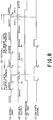
- FIG. 8 is a time chart according to the present embodiment. Parts (A), (B), (C) and (D) of FIG. 8 show serial data, driver output, depression condition of SW 2 and SW-DATA signal, respectively. The operation will be described hereinafter referring to the figure.
- the driver electronics 11 shown in FIG. 5 receives, on DATA input terminal, LED data (FFFF)H transmitted from CPU 13, the driver electronics 11 including a shifter, not shown, serves to sequentially store in the shifter data in synchronism with serial clock signals also supplied from CPU 13.
- the LED data (FFFF)H have been stored in its entirety in the shifter and are output in parallel from the output terminals O1 - O16.
- the operating switch SW 2 is depressed.
- SW sense data (0080)H as the serial signal are entered to the driver electronics 11.
- the SW sense data (0080)H have been stored in its entirety in the shifter and are output in parallel from the output terminals O1 - O16 as shown in part (A) of FIG. 7.
- CPU 13 is able to sense the condition of switch SW 1 by means of sensing of SW-DATA signal in level binary "1" or "0". According to the embodiment of FIG. 8, since switch SW 1 is not depressed, SW-DATA signal is binary "0" in level.
- CPU 13 senses that switch SW 1 is not depressed.
- SW sense data (0040)H in the form of the serial signal is entered to the driver IC 11.
- the SW sense data (0040)H have been stored in its entirety in the shifter and are output in parallel from the output terminals O1 - O16 as shown in part (B) of FIG. 7.
- the current flows through the output terminal O10 and then SW-DATA signal becomes binary "1" in level.
- CPU 13 senses that switch SW 2 is in its depressed condition.
- switches SW 3 - SW 8 are sensed.
- LED data (FFFF)H is again entered, and light emitting diodes LED 1 - LED 16 are lighted.
- the illustrative embodiments include a light emitting diode as the display or indicator means. It should be noted, however, that an incandescent lamp may also be used as the display means for a light emitting diode since the sufficient current required for the incandescent lamp is supplied by the driver.
- the resistance as a switch condition sensing means.
- any sort of device may be used which is adapted for sensing current or voltage on a switch to be detected.
- a small size of electromagnet instead of the resistance, is provided, and a reed switch between the both ends of which a predetermined voltage is applied is disposed near the electromagnet, wherein a voltage is detected when the electromagnet is operated, so that terminals of the reed switch make contact with each other.
- the number of signal wires between the CPU and the printed circuit board is remarkably reduced, and thus it is possible to reduce the number of circuit connection patterns provided on the circuit board, thereby minimizing the area of the printed circuit board.
Landscapes
- Engineering & Computer Science (AREA)
- Physics & Mathematics (AREA)
- Computer Hardware Design (AREA)
- General Physics & Mathematics (AREA)
- Theoretical Computer Science (AREA)
- Control Of Indicators Other Than Cathode Ray Tubes (AREA)
- Control Of El Displays (AREA)
- Accessory Devices And Overall Control Thereof (AREA)
Applications Claiming Priority (4)
| Application Number | Priority Date | Filing Date | Title |
|---|---|---|---|
| JP2296602A JPH04168594A (ja) | 1990-10-31 | 1990-10-31 | 表示制御回路 |
| JP296602/90 | 1990-10-31 | ||
| JP325826/90 | 1990-11-29 | ||
| JP32582690A JPH04205099A (ja) | 1990-11-29 | 1990-11-29 | 制御回路 |
Publications (2)
| Publication Number | Publication Date |
|---|---|
| EP0483829A2 true EP0483829A2 (fr) | 1992-05-06 |
| EP0483829A3 EP0483829A3 (en) | 1992-12-23 |
Family
ID=26560749
Family Applications (1)
| Application Number | Title | Priority Date | Filing Date |
|---|---|---|---|
| EP19910118565 Withdrawn EP0483829A3 (en) | 1990-10-31 | 1991-10-30 | Control circuit for operating panel |
Country Status (1)
| Country | Link |
|---|---|
| EP (1) | EP0483829A3 (fr) |
Cited By (1)
| Publication number | Priority date | Publication date | Assignee | Title |
|---|---|---|---|---|
| CN102779480A (zh) * | 2012-08-17 | 2012-11-14 | 深圳市易事达电子有限公司 | 显示屏驱动电路及发光二极管显示装置 |
Family Cites Families (2)
| Publication number | Priority date | Publication date | Assignee | Title |
|---|---|---|---|---|
| JPS5271152A (en) * | 1975-12-10 | 1977-06-14 | Seiko Epson Corp | Computer |
| DE3116941A1 (de) * | 1981-04-29 | 1982-11-25 | Matth. Hohner Ag, 7218 Trossingen | "schaltungsanordnung mit einem tastschalterblock" |
-
1991
- 1991-10-30 EP EP19910118565 patent/EP0483829A3/en not_active Withdrawn
Cited By (2)
| Publication number | Priority date | Publication date | Assignee | Title |
|---|---|---|---|---|
| CN102779480A (zh) * | 2012-08-17 | 2012-11-14 | 深圳市易事达电子有限公司 | 显示屏驱动电路及发光二极管显示装置 |
| CN102779480B (zh) * | 2012-08-17 | 2015-04-15 | 深圳市易事达电子股份有限公司 | 显示屏驱动电路及发光二极管显示装置 |
Also Published As
| Publication number | Publication date |
|---|---|
| EP0483829A3 (en) | 1992-12-23 |
Similar Documents
| Publication | Publication Date | Title |
|---|---|---|
| US6255960B1 (en) | System and method for programming display characteristics of an LED of an electrical appliance | |
| EP1106368B1 (fr) | Imprimante, méthode de contrôle associée et support de stockage de données | |
| EP0910090B1 (fr) | Connection d'interface pour machine hôte | |
| EP0217043A1 (fr) | Dispositif de détection d'erreurs dans le circuit de chauffage d'une tête d'impression thermique | |
| EP0483829A2 (fr) | Circuit de contrôle pour afficheur | |
| US5431505A (en) | Operating environment setting system and method for printer | |
| JPH0315703B2 (fr) | ||
| US5581201A (en) | Apparatus for unit control and presence detection | |
| EP0301100A1 (fr) | Circuit d'alimentation | |
| US5936819A (en) | Break display apparatus for semiconductor switching element incorporating overcurrent/overheating protection function | |
| EP0597600B1 (fr) | Dispositif indicateur d'état pour une imprimante | |
| JPH0615311Y2 (ja) | 入力装置 | |
| KR20010045148A (ko) | 고장 점검기능을 갖는 전광판용 표시모듈 | |
| JPH04205099A (ja) | 制御回路 | |
| JPH0710789U (ja) | 発光素子輝度調整装置 | |
| CN215374225U (zh) | 用于检测控制板上发光二极管的装置 | |
| US4315250A (en) | Connection arrangement for selection and display system | |
| JPH0692181B2 (ja) | 紙詰まり検出機能付きプリンタ | |
| KR950007838Y1 (ko) | 데이타 충돌 표시 장치 | |
| JP2681078B2 (ja) | センサ装置 | |
| SU1137455A1 (ru) | Устройство дл индикации | |
| JPS59104692A (ja) | 電子機器 | |
| JPH10221112A (ja) | 初期設定回路 | |
| JP2502012B2 (ja) | スイッチ状態検出装置 | |
| JP2940509B2 (ja) | データ検出回路 |
Legal Events
| Date | Code | Title | Description |
|---|---|---|---|
| PUAI | Public reference made under article 153(3) epc to a published international application that has entered the european phase |
Free format text: ORIGINAL CODE: 0009012 |
|
| AK | Designated contracting states |
Kind code of ref document: A2 Designated state(s): DE FR GB |
|
| PUAL | Search report despatched |
Free format text: ORIGINAL CODE: 0009013 |
|
| AK | Designated contracting states |
Kind code of ref document: A3 Designated state(s): DE FR GB |
|
| 17P | Request for examination filed |
Effective date: 19930222 |
|
| STAA | Information on the status of an ep patent application or granted ep patent |
Free format text: STATUS: THE APPLICATION HAS BEEN WITHDRAWN |
|
| 18W | Application withdrawn |
Withdrawal date: 19930528 |