EP0301100A1 - Circuit d'alimentation - Google Patents
Circuit d'alimentation Download PDFInfo
- Publication number
- EP0301100A1 EP0301100A1 EP88901321A EP88901321A EP0301100A1 EP 0301100 A1 EP0301100 A1 EP 0301100A1 EP 88901321 A EP88901321 A EP 88901321A EP 88901321 A EP88901321 A EP 88901321A EP 0301100 A1 EP0301100 A1 EP 0301100A1
- Authority
- EP
- European Patent Office
- Prior art keywords
- current path
- power supply
- resistor
- time
- controller
- Prior art date
- Legal status (The legal status is an assumption and is not a legal conclusion. Google has not performed a legal analysis and makes no representation as to the accuracy of the status listed.)
- Withdrawn
Links
Images

Classifications
-
- G—PHYSICS
- G06—COMPUTING OR CALCULATING; COUNTING
- G06F—ELECTRIC DIGITAL DATA PROCESSING
- G06F1/00—Details not covered by groups G06F3/00 - G06F13/00 and G06F21/00
- G06F1/26—Power supply means, e.g. regulation thereof
Definitions
- the present invention relates to a power supply circuit.
- General keyboard units used as input equipment in computer systems or word processors are provided with indication functions by light emission, to inform an operator of various states of the keyboard, or of the systems wherein the keyboard units are used, for example, "SYSTFM READY", “POWER ON”, “HOLD”. "FAULT” and the like, in addition to keys for letters and numerals and the like, and key switches corresponding to the keys.
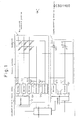
- FIG. 1 is a simplified diagram of a conventional keyboard unit.
- the keyboard unit shown in Fig.1 consists of a keyboard comprising a plurality of key switches 11 which are placed in correspondence to keys and form a matrix, and light-emitting devices (LED) 21-l, 21-2; a printed circuit board (PCB) comprising a controller 3, a decoder 10, drivers 12-1, 12-2. 12-3, 22-1, 22-2, receivers 13-1, 13-2, resistors 4-1, 4-2, 4-3, 4-4, and an output register 20; and wiring portions comprising wires connecting the keyboard and the PCB.
- a keyboard comprising a plurality of key switches 11 which are placed in correspondence to keys and form a matrix, and light-emitting devices (LED) 21-l, 21-2
- PCB printed circuit board
- the keyboard unit is divided into a key switch read-out portion 1 ' for reading the key switches 11, a light-emitting display portion 2 ' having a display function of informing an operator of the aforementioned various states by light emission, and a controller 3 controlling the key switch read-out portion 1 ' and the light-emitting display portion 2' .
- a key switch read-out portion 1 ' for reading the key switches 11
- a light-emitting display portion 2 ' having a display function of informing an operator of the aforementioned various states by light emission
- a controller 3 controlling the key switch read-out portion 1 ' and the light-emitting display portion 2' .
- the controller 3. which has a microprocessor. outputs a key address signal to the key switch read out portion 1 ' for reading out which key is pushed, and receives the results of the reading.
- the controller 3 also controls the light emission by the LEDs 21-2, 21-2 in the light-emitting display portion 2.
- the key switch read-out portion 1 comprises: a plurality of key switches 11 which are placed in correspondence to the keys and form a matrix; the diodes accompanying the key switches; drivers 12-1, 12-2, 12-3 provided in correspondence to the lines of the matrix: the receivers 13-1, 13-2 provided in correspondence to the rows of the matrix; the resistors 4-1, 4-2, each of which is connected at one terminal to the input side of the corresponding one of the receivers 13-1. 13-2. and at the other terminal to a voltage source of a higher voltage (+5V): and a decoder 10.
- One end of each key switch 11 in each line of the matrix is connected through a diode to the output of the corresponding one of the drivers 12-1, 12-2, 12-3. and the other end of each key switch 11 in each row of the matrix is connected to the input of the corresponding one of the receivers 13-1, 13-2.
- the aforementioned key address signal from the controller 3 selects one of the drivers 12-1, 12-2, 12-3, each of which corresponds to one of the lines in the matrix.
- the meanings of the key address signal is decoded at the decoder 10, and the decoder 10 outputs a drive input to the selected driver among the drivers 12-1, 12-2, 12-3.
- the output of the selected driver among the drivers 12-1. 12-2, 12-3 is brought to a lower voltage level.
- the diodes connected in series to the key switches 11 are provided to prevent a misreading due to the forming of a plurality of the circuits through a plurality of the key switches when a plurality of the key switches are operated at the same time.
- the aforementioned light-emitting display portion 2 comprises the output register 20, the drivers 22-1, 22-2 for the light-emitting devices ( LED ) 21-1, 21-2. the light-emitting devices ( LED ) 21-1, 21-2, and the resistors 4-3, 4-4.
- a command for an on-and-off control of each of the LEDs 21-1, 21-2 from the controller 3 is sent through the output register 20 to the drivers 22-1. 22-2.
- the output of each of the drivers 22-1, 22-2 is brought to the lower level.
- Each output of the drivers 22-1 : 22-2 is connected through the corresponding one of the resistors 4-3, 4-4 to one end of the corresponding one of the LEDs 21-1, 21-2, and the other ends thereof are connected to a voltage source of a higer voltage +5V. Therefore, when the output of any of the drivers 22-1, 22-2 is brought to the lower voltage, the corresponding LED 21-1, 21-2 is turned on and emits light.
- the outputs of the drivers 22-1, 22-2 which do not receive the command from the controller 3 remain at the higher level, and therefore, the corresponding LEDs 21-1, 21-2, which are connected through the corresponding resistors 4-3, 4-4 to the outputs of the drivers 22-1, 22-2. are not turned on. and do not emit light.
- the resistors 4-1, 4-2 are provided at the input side of the receivers 1.3- 1 13-2 in the key switch read-out portion 1' and the inputs of the receivers 13-1. 13-2 are connected through the resistors 4 -1, 4-2 to the +5V voltage source.
- the light-emitting display portion 2 ' one end of each of the LEDs 21-1. 21-2 is connected to the corresponding one of the resistors 4-3, 4-4, and the other end is connected to the +5V voltage source.
- each of the LED 21-1. 21-2 is connected to the input level of the corresponding one of the receivers 13-1. 13-2 when one of the LEDs 21-1, 21-2 is turned on.
- the input level of the corresponding one of the receivers 13-1. 13-2 becomes lower than the +5V level due to a voltage drop through the corresponding one of the resistors 4 -1 - 4-2. and this may prevent a correct detection hy the receivers 13-1. 13-2 of the OFF state of the key switch 11.
- An object of the present invention is to provide a power supply circuit by which it is possible to supply electric power from a common power source through a common resistor, without the influence of a voltage drop, to both a current path which needs a power supply for at least a predetermined time and another current path which allows a break of a power supply for at least the predetermined time, to lower the number of the parts constituting the power supply circuit itself, and reduce the scale of the circuit.
- a power supply circuit comprises: a first current path which needs a power supply for at least a predetermined time and a second current path which allows a break of a power supply for at least the predetermined time; a voltage from a power source is applied through a resistor in parallel to one end of each of the first and second current paths; each of the first and second current paths having first and second driver circuits, respectively, each of which driver circuits controls a current from the power source in the corresponding current path; each of the first and second driver circuits is driven alternatively by a controller; the controller controls the on-and-off timings of the first and second driver circuits so that the first current path is maintained in the ON state for a time equal to or more than the time needed, and the second current path is broken for a time equal to or less than the time allowed.
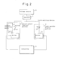
- Figure 2 shows the basic construction of the present invention.
- reference numeral is a first current path
- 2 is a second current path.
- 3 is a controller
- 4 is a resistor
- 5 is a voltage source.
- the resistor 4 is connected at one end to the power source 5, and at the other end to one end of each of the first and second current paths 1, 2.
- Each of the first and second current paths 1, 2 has first and second driver circuits 12, 22, respectively, and the first and second driver circuits 12, 22 are driven alternatively hy a controller 3.
- the first current 1 path needs a power supply for at least a predetermined time and a second current path 2 allows a break of a power supply for at least the predetermined time.
- the controller controls the on-and-off timings of the first and second driver circuits 12. 22 so that the first current path is maintained in the ON state for a time equal to or more than the time needed, and the second current path 2 is broken for a time equal to or less than the time allowed.
- the abovementioned construction makes it possible to supply an electric power from a common power source through a common resistor, without the influence of a voltage drop, to both a current path which needs a power supply for at least a predetermined time and aother current path which allows a break of a power supply for at least a predetermined time, lowers the number of parts constituting the power supply circuit itself, and reduces the scale of the circuit smaller.
- Fig. 2 shows, in a circle 1 by a dashed line. a construction wherein a switch 11 is connected between the first driver circuit 12 and the resistor 4 in the first current path 1, and a voltage detecting means 13 which detects a voltage at the resistor 4 side of the switch 11 is provided, and accordingly, a switch on/off detecting circuit is constructed.
- Fig. 2 shows, in a circle 2 by another dashed line, a construction wherein a light-emitting device 21 is connected between the second driver circuit 22 and the resistor 4 in the second current path 2. and a light-emitting device driving circuit is realized.
- Fig. 2 makes it possible to supply an electric power from a common power source through a common resistor in a time-sharing manner. without the influence of a voltage drop, to both the switch on/off detecting circuit 1 and the light-emitting device driving circuit 2, because the time necessary to supply power intermittently to the switch on/off detecting circuit (the first current path) 1 by driving the first driver circuit 12 to detect whether the switch is opened or closed in the switch on/off detecting circuit (the first current path) 1, is much shorter than the time allowed for the light-emitting device driving circuit (the second current path) 2 to break, i.e., the time necessary to break the current in the light-emitting device driving circuit (the second current path) 2, is so short that the break cannot be seen by the naked eye.
- FIG. 3 is a simplified diagram of the construction of a keyboard equipment according to the present invention.
- Fig. 3 Although much of the basic construction shown in Fig. 3 is the same as the corresponding construction of Fig. 1. differences exist first in that the terminals at the higher voltage sides of the LEDs 21-1. 21-2 in the light emiting display portion 2 ' are connected to the input levels of the receivers 13-1. 13-2 (which correspond to the voltage detecting circuit 13 in Fig. 2) in the key switch read-out portion 1 ; second in that the read key signal from the controller 3 is applied to an input terminal of the decoder 10 in the key switch read-out portion 1 as a signal to enable the output of the decoder 10: and third in that the above read key signal is also applied to disable the aforementioned drivers 22-1, 22-2 for the LEDs in the light-emitting display portion 2.
- the outputs of all the drivers 12-1. 12-2. 12-3 remain at the higher level. and the inputs of the receivers 13-1: 13-2 are +5V. In this situation. if a command to emit a light is output from the controller 3. i.e,. if the bit corresponding to the LED 21-1 or 21-2- which should emit a a light.. of the output register 20 becomes "1''.
- the output of the corresponding drivers 22 1, 22-2 for the LEDs in the light-emitting display portion 2 is brought to the lower level, because one input of each NAND circuit which realizes one or the other of the drivers 22-1. 22-2 for the LEDs is the read key signal which is at the higher level, and the other input of the corresponding NAND circuit is at the higher level as the corresponding bit of the output register 20 is "1".
- the resistor connected at the one end to the LED which should emit light among the resistors 4-1 and 4-2 in the key switch read-out portion, the current flows from the +5V voltage source to the LED 21-1 or 21-2. and accordingly, the LED 21-1 or 21 -2 emits light.
- the controller 3 When the controller 3 reads the states of the kev switch 11 in the key switch read-out portion l' the controller 3 commands which driver among the drivers 12-1, 12-2, 12-3 should be driven by the aforementioned key address signal, and brings the read key signal to the lower level. Accordingly, the decoder 10 is enabled, and the driver (12-1, 12-2, or 12-3) commanded by the key address signal is driven, and therefore, the output of the driver is brought to the lower level.
- the read key signal which has been brought to the lower level is applied to each of the drivers 22-1, 22-2 for the LEDs in the light-emitting display portion 2 to bring one input of each of the NAND circuits to the lower level, and then holds the outputs of all the drivers 22-1, 22-2. 22-3 at the higher level. i.e.. disables the drivers 22-1. 22-2. and thus no current flows in any LED during the operation of the key switch read-out portion 1 .
- the key switch 11 is OFF. no voltage drop occurs in the resistors 4-1, 4-2 in the key switch read-out portion 1 , and the input levels of the receivers 13-1. 13-2 remain at the higher level (+5V), and therefore.
- a smaller number of parts is used than in the conventional keyboard equipment, but a keyboard equipment having the same function as the conventional keyboard equipment can be realized.
- the power supply circuit according to the present invention is useful in systems having a plurality of circuits each of which circuits can be operated by supplying an electric current in a time-sharing manner.
Landscapes
- Engineering & Computer Science (AREA)
- Theoretical Computer Science (AREA)
- Physics & Mathematics (AREA)
- General Engineering & Computer Science (AREA)
- General Physics & Mathematics (AREA)
- Input From Keyboards Or The Like (AREA)
- Control Of Indicators Other Than Cathode Ray Tubes (AREA)
Abstract
Circuit d'alimentation fournissant un courant électrique à une pluralité de circuits tout à tour. Le circuit d'alimentation comprend une source de tension (5), une résistance (4) reliée par une extrémité à la source de tension (5), un premier passage de courant (1) relié par une extrémité à l'autre extrémité de la résistance (4) et comprenant un premier circuit régulateur (12), un deuxième passage de courant (2) relié par une extrémité à l'autre extrémité de la résistance (4) et comprenant un deuxième circuit régulateur (22), et un circuit de commande (3) qui commande alternativement les premier et deuxième circuits régulateurs (12, 22). Ce circuit de commande (3) fait varier les intervalles de régulation des premier et deuxième circuits régulateurs (12, 22) de sorte que le premier passage de courant (1) est conducteur pendant une période de temps plus longue que la période requise et que le deuxième passage de courant (22) est interrompu pendant une période de temps plus courte que la période admissible.
Applications Claiming Priority (2)
| Application Number | Priority Date | Filing Date | Title |
|---|---|---|---|
| JP30676/87 | 1987-02-14 | ||
| JP62030676A JPS63200224A (ja) | 1987-02-14 | 1987-02-14 | キ−ボ−ド装置 |
Publications (2)
| Publication Number | Publication Date |
|---|---|
| EP0301100A1 true EP0301100A1 (fr) | 1989-02-01 |
| EP0301100A4 EP0301100A4 (en) | 1992-08-19 |
Family
ID=12310314
Family Applications (1)
| Application Number | Title | Priority Date | Filing Date |
|---|---|---|---|
| EP19880901321 Withdrawn EP0301100A4 (en) | 1987-02-14 | 1988-02-02 | Power supply circuit |
Country Status (4)
| Country | Link |
|---|---|
| US (1) | US5006728A (fr) |
| EP (1) | EP0301100A4 (fr) |
| JP (1) | JPS63200224A (fr) |
| WO (1) | WO1988006316A1 (fr) |
Cited By (1)
| Publication number | Priority date | Publication date | Assignee | Title |
|---|---|---|---|---|
| EP0429780A3 (en) * | 1989-11-29 | 1994-08-24 | Toshiba Kk | Computer system capable of connecting expansion unit |
Families Citing this family (5)
| Publication number | Priority date | Publication date | Assignee | Title |
|---|---|---|---|---|
| KR940000392B1 (ko) * | 1991-01-18 | 1994-01-19 | 삼천전기 주식회사 | 전력 반송 주파수 차단기 |
| CA2089642A1 (fr) * | 1991-06-28 | 1992-12-29 | Ronald J. Bilas | Systeme de distribution electrique a circuit de commande ameliore de disjoncteurs multiples |
| KR960002930B1 (ko) * | 1992-11-23 | 1996-02-28 | 삼성전자주식회사 | 입출력신호가 동일 단자에서 구현되는 스위칭회로 |
| DE59510512D1 (de) * | 1994-07-27 | 2003-01-30 | Philips Corp Intellectual Pty | Schaltungsanordnung mit wenigstens einer aus einer Spannungsquelle zu speisenden Stufe |
| WO2021199443A1 (fr) * | 2020-04-03 | 2021-10-07 | オリンパス株式会社 | Élément d'imagerie, endoscope, système d'endoscope et procédé d'inspection |
Family Cites Families (16)
| Publication number | Priority date | Publication date | Assignee | Title |
|---|---|---|---|---|
| US3104323A (en) * | 1961-10-30 | 1963-09-17 | Jr John J Over | Light sensitive two state switching circuit |
| US3705342A (en) * | 1971-06-21 | 1972-12-05 | Metrodata Corp | Dc voltage regulator and impedance converter |
| US4137557A (en) * | 1974-05-15 | 1979-01-30 | Societa Italiana Vetro S/V S.P.A. | Automatic cut-out device |
| JPS53142825A (en) * | 1977-05-18 | 1978-12-12 | Fujitsu Ltd | Keyboard display system |
| JPS57193964A (en) * | 1981-05-20 | 1982-11-29 | Toshiba Corp | Switching device |
| US4421993A (en) * | 1982-05-28 | 1983-12-20 | General Electric Company | Load resistance control circuitry |
| DE3240778A1 (de) * | 1982-11-04 | 1984-05-10 | Siemens AG, 1000 Berlin und 8000 München | Elektronischer schalter |
| JPS59178735U (ja) * | 1983-05-11 | 1984-11-29 | 三洋電機株式会社 | 表示装置 |
| US4585986A (en) * | 1983-11-29 | 1986-04-29 | The United States Of America As Represented By The Department Of Energy | DC switching regulated power supply for driving an inductive load |
| JPS61156423A (ja) * | 1984-12-28 | 1986-07-16 | Toshiba Corp | マイクロコンピユ−タのキ−スキヤン方式 |
| US4616142A (en) * | 1984-12-31 | 1986-10-07 | Sundstrand Corporation | Method of operating parallel-connected semiconductor switch elements |
| US4659942A (en) * | 1985-06-03 | 1987-04-21 | The Charles Stark Draper Laboratory, Inc. | Fault-tolerant power distribution system |
| JPS61279918A (ja) * | 1985-06-05 | 1986-12-10 | Alps Electric Co Ltd | 入力表示制御装置 |
| JPS61296420A (ja) * | 1985-06-25 | 1986-12-27 | Casio Comput Co Ltd | 小型電子式計算機 |
| US4827366A (en) * | 1986-12-05 | 1989-05-02 | Mcnally Paul F | Bi-polar power supply regulator bi-polar power supply regulator |
| US4929936A (en) * | 1988-03-21 | 1990-05-29 | Home Security Systems, Inc. | LED illuminated sign |
-
1987
- 1987-02-14 JP JP62030676A patent/JPS63200224A/ja active Granted
-
1988
- 1988-02-02 EP EP19880901321 patent/EP0301100A4/en not_active Withdrawn
- 1988-02-02 WO PCT/JP1988/000091 patent/WO1988006316A1/fr not_active Ceased
-
1990
- 1990-04-23 US US07/511,897 patent/US5006728A/en not_active Expired - Fee Related
Non-Patent Citations (2)
| Title |
|---|
| No relevant documents disclosed * |
| See also references of WO8806316A1 * |
Cited By (3)
| Publication number | Priority date | Publication date | Assignee | Title |
|---|---|---|---|---|
| EP0429780A3 (en) * | 1989-11-29 | 1994-08-24 | Toshiba Kk | Computer system capable of connecting expansion unit |
| US5428798A (en) * | 1989-11-29 | 1995-06-27 | Kabushiki Kaisha Toshiba | Computer system capable of connecting expansion unit |
| US5440748A (en) * | 1989-11-29 | 1995-08-08 | Kabushiki Kaisha Toshiba | Computer system capable of connecting expansion unit |
Also Published As
| Publication number | Publication date |
|---|---|
| EP0301100A4 (en) | 1992-08-19 |
| US5006728A (en) | 1991-04-09 |
| JPS63200224A (ja) | 1988-08-18 |
| WO1988006316A1 (fr) | 1988-08-25 |
| JPH0423288B2 (fr) | 1992-04-21 |
Similar Documents
| Publication | Publication Date | Title |
|---|---|---|
| US5083063A (en) | Radiation generator control apparatus | |
| CN100553363C (zh) | 操作开关布线机构 | |
| CA1216650A (fr) | Installation de commande pour rayons de stockage mobile | |
| EP0301100A1 (fr) | Circuit d'alimentation | |
| EP2096898A1 (fr) | Système d'éclairage à DEL pour véhicules avec dispositif de contrôle et de diagnostic | |
| US7259683B2 (en) | Rack | |
| JPH0643830A (ja) | 表示装置の輝度制御回路 | |
| EP0079743B1 (fr) | Test de fonctionnement d'un redresseur commandé | |
| US4611271A (en) | Control system with a microprocessor | |
| AU710036B2 (en) | A display apparatus for programmable logic controllers | |
| US5400021A (en) | Apparatus for controlling an operational panel | |
| JP2549954B2 (ja) | 発光ダイオードの駆動装置 | |
| EP0597600A2 (fr) | Dispositif indicateur d'état pour une imprimante | |
| EP0392658A2 (fr) | Circuit de commande pour machines de jeux actionnées par pièces de monnaie | |
| JP2001283712A (ja) | ヒューズ断線監視装置 | |
| JPS6341480B2 (fr) | ||
| KR102232870B1 (ko) | 터널등 제어 회로 및 이의 작동 방법 | |
| US5675747A (en) | Data transmission system with erroneous connection indicator | |
| JP2002051389A (ja) | リモートコントロール用回路 | |
| KR200185471Y1 (ko) | 마이컴의 포트 셀렉터 | |
| JPH0417455B2 (fr) | ||
| JP3121236B2 (ja) | Led標識灯システム | |
| KR930011811B1 (ko) | 고기능 전기 전자 오븐 제어장치의 일출력회로 | |
| JPH09326683A (ja) | 入力または出力のための装置 | |
| JPS61277331A (ja) | 操作盤の制御方法 |
Legal Events
| Date | Code | Title | Description |
|---|---|---|---|
| PUAI | Public reference made under article 153(3) epc to a published international application that has entered the european phase |
Free format text: ORIGINAL CODE: 0009012 |
|
| 17P | Request for examination filed |
Effective date: 19881018 |
|
| AK | Designated contracting states |
Kind code of ref document: A1 Designated state(s): DE FR GB |
|
| A4 | Supplementary search report drawn up and despatched |
Effective date: 19920703 |
|
| AK | Designated contracting states |
Kind code of ref document: A4 Designated state(s): DE FR GB |
|
| STAA | Information on the status of an ep patent application or granted ep patent |
Free format text: STATUS: THE APPLICATION IS DEEMED TO BE WITHDRAWN |
|
| 18D | Application deemed to be withdrawn |
Effective date: 19890802 |