EP0484011A2 - Verpackung von optischen Komponenten aus Silizium - Google Patents
Verpackung von optischen Komponenten aus Silizium Download PDFInfo
- Publication number
- EP0484011A2 EP0484011A2 EP91309593A EP91309593A EP0484011A2 EP 0484011 A2 EP0484011 A2 EP 0484011A2 EP 91309593 A EP91309593 A EP 91309593A EP 91309593 A EP91309593 A EP 91309593A EP 0484011 A2 EP0484011 A2 EP 0484011A2
- Authority
- EP
- European Patent Office
- Prior art keywords
- waveguide
- coverplate
- optical
- epoxy
- layer
- Prior art date
- Legal status (The legal status is an assumption and is not a legal conclusion. Google has not performed a legal analysis and makes no representation as to the accuracy of the status listed.)
- Granted
Links
Images


Classifications
-
- G—PHYSICS
- G02—OPTICS
- G02B—OPTICAL ELEMENTS, SYSTEMS OR APPARATUS
- G02B6/00—Light guides; Structural details of arrangements comprising light guides and other optical elements, e.g. couplings
- G02B6/24—Coupling light guides
- G02B6/26—Optical coupling means
- G02B6/30—Optical coupling means for use between fibre and thin-film device
-
- G—PHYSICS
- G02—OPTICS
- G02B—OPTICAL ELEMENTS, SYSTEMS OR APPARATUS
- G02B6/00—Light guides; Structural details of arrangements comprising light guides and other optical elements, e.g. couplings
- G02B6/24—Coupling light guides
- G02B6/26—Optical coupling means
- G02B6/28—Optical coupling means having data bus means, i.e. plural waveguides interconnected and providing an inherently bidirectional system by mixing and splitting signals
- G02B6/2804—Optical coupling means having data bus means, i.e. plural waveguides interconnected and providing an inherently bidirectional system by mixing and splitting signals forming multipart couplers without wavelength selective elements, e.g. "T" couplers, star couplers
- G02B6/2808—Optical coupling means having data bus means, i.e. plural waveguides interconnected and providing an inherently bidirectional system by mixing and splitting signals forming multipart couplers without wavelength selective elements, e.g. "T" couplers, star couplers using a mixing element which evenly distributes an input signal over a number of outputs
Definitions
- the present invention relates to integrated optical components and, more particularly, to optical components fabricated on silicon substrates.
- the cladding layer which is about 4 ⁇ m thick does not provide sufficient optical confinement for the evanescent field radially extending from core, thereby allowing it to deleteriously interact with the environment. For example, touching the upper surface of the component dramatically changes the device performance. Although a much thicker cladding layer could be deposited, on the order of approximately 10 ⁇ m, such a thick coating either tends to crack due to stress or prohibitively takes a very long time, on the order of a day, to deposit.
- This invention is a new optical packaging and interconnection technology which is particularly effective in not only addressing the problem of attaching fiber pigtails to glass waveguide silicon devices, but also in isolating these waveguide devices from the deleterious effects of their external environment.
- An important aspect of the invention lies in the novel realization that the foregoing objectives may be achieved by covering the device with a thin silica coverplate affixed with a low index epoxy, which extends the cladding layer of the waveguides such that the evanescent field does not interact with the environment.
- the silica coverplate serves to "ruggedize" the device while providing end surfaces of sufficient area to which pigtailed fiber connectors can be attached.
- an integrated 19 x 19 star coupler formed on a silicon substrate is covered with a silica coverplate attached by means of a low index epoxy.
- the coverplate both isolates the waveguides, which are approximately a few microns below the surface, from their surrounding and moreover, provides an enhanced means for attaching fiber connectors thereto.
- the present invention is based upon the discovery that by covering glass waveguide silicon devices with a thin silica (SiO2) coverplate affixed with a low index epoxy, it is possible to isolate these devices from external effects and at the same time provide an enhanced means for attaching fiber connectors thereto.
- low index epoxy as used herein means an epoxy resin the index of refraction of which is lower than the index of refraction of the waveguide core of the device, equal or lower then the index of refraction of the cladding layer surrounding the waveguide core of the device or both.
- the low index epoxy forms an extended cladding layer which provides enhanced optical confinement in the waveguide core.
- the silica coverplate which is held by the epoxy serves to "ruggedize" the device and provide end surfaces to which pigtailed fiber connectors can be attached.
- FIG. 1 One exemplary embodiment of an optical device according to the principles of the invention is depicted in FIG. 1. While the proceeding description relates to the depicted star coupler, which is fabricated using the prior art silica on silicon technology, it should be understood that other silica on silicon waveguide devices may be used, such as Bragg reflectors, multiplexers, splitters and the like, which are well known in the art. Furthermore, it is contemplated that these optical devices may be fabricated directly on fused quartz, silica, lithium niobate and the like. Accordingly, it should be understood that the integrated optical device shown in FIG. 1 is only for the purpose of illustration and not for the purpose of limitation
- FIG. 1 shown in FIG. 1 is a planar view for the geometry of an integrated 19 x 19 star coupler 10, consisting of two symmetric arrays of channel waveguides 20, 30 separated by a dielectric slab waveguide 60, each formed on silicon (Si) substrate 40.
- Conventional well known fabrication techniques such as lithography, etching, low pressure vapor chemical deposition, flame hydrolysis and the like, may be used to fabricate star coupler 10.
- glass waveguides on silicon and the processing therein see C. H. Henry et al., Journal of Lightwave Technology, Vol. 7, No. 10 pp. 1530-9 (1989) and B. H. Verbeek et al., Journal Of Lightwave Technology, Vol., 6, No. 6 pp. 1011-15 (1988).
- silica coverplate 310 has been affixed on top of cladding layer 203 with a low index epoxy to obviate the foregoing problems. With silica coverplate 310 held in place by the epoxy, end surfaces are afforded to which pigtailed fiber connectors can be attached.
- waveguides 20-1 through 20-19 and 30-1 through 30-19 comprise a 10 ⁇ m thick SiO2 base layer 201 formed by oxidizing the surface of silicon substrate 40 in a high pressure steam.
- Both core and cladding layers 202 and 203, respectively, were deposited using low pressure chemical vapor depositions. More specifically, a 2 ⁇ m thick phosphosilicate glass (8 % weight Phosphorus), deposited using silane, oxygen and phosphine, was used as core layers 202, with 5 ⁇ m wide mesas subsequently etched by reactive ion etching after photolithographically defining core 202.
- the core layers were annealed at 1000° C in N2 in order to reflow the material.
- a 3 ⁇ m thick top or cladding layer 203 of SiO2 (4% weight Phosphorus) was deposited at 730° C using tetraethylorthosilicate (TEOS), oxygen and phosphine.
- TEOS tetraethylorthosilicate
- the resulting refractive index difference between core layers 202 and cladding layer 203 was estimated to be 7.3 x 10 ⁇ 3 for a wavelength ⁇ of 1.5 ⁇ m, with the cladding layer having a refractive index of approximately 1.456.
- the choice in the value of the refractive index difference between the core and cladding layers is predicated upon factors such as wavelength of operation, desired numerical aperture, and the desired number of modes, as well as other factors.
- silica coverplate 310 was fused silica having an index of refraction n of approximately 1.456.
- low refractive index epoxy 300 is interposed between silica coverplate 310 and the waveguides in order not to extract energy from cores 202 thereof. That is, optical epoxy 300 cannot have a higher index of refraction than that of silica cladding layer 203.
- a two component heat curing epoxy having an index of refraction n exp of 1.4071 was utilized, such as the epoxy sold by Epoxy Technology, Inc., Billerica, MA, designated by its tradename EPO-TEX 328.
- This epoxy has a medium viscosity of 3500 cps as well as good weting characteristics and transparent properties.
- the epoxy was applied by wicking it between cladding layer 203 and silica coverplate 310, thereby resulting in the configuration shown in FIG. 2. Subsequently, the epoxy was cured at 150 °C leaving a thin epoxy layer of about 10 ⁇ m which adheres silica coverplate 310 to the top surface of the waveguides.
- silica coverplate 310 was cut to the same dimensions and, then, the ends thereof polished. Coverplate 310 had approximately a thickness of 0.65 mm.
- fiber pigtail connectors 420 and 410 each comprised a linear array of fibers positioned within v-grooves fabricated on the top surface of silicon chips 440.
- Such fiber pigtail connectors are well known in the art and not discussed here. However, for a detailed discussion of these optical connectors, see for example, the patent of E. J. Murphy cited aboveherein.
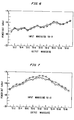
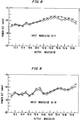
- FIGs. 4 through 6 show the performance of star coupler 10 before and after covering the waveguides with silica coverplate 310, and with input waveguides 20-1, 20-10 and 20-19 each separately excited with horizontally polarized light having a wavelength of approximately 1.3 ⁇ m. It should be noted that measurements made before affixing silica coverplate 310 are designated by open circles whereas measurements made after afixing the silica coverplate 310 are designated by crosses.
- the splitting loss of the star coupler 10 which is proportional to 1/N (where N the number of input or output waveguides), should in this case be approximately 12.8 dB.
- the loss before and after affixing silica coverplate 310 is substantially identical. It is believed that the coupling loss between the central input waveguide 50-10 and the output waveguides, which is about 2 dB more than the ideal coupler, can be accounted for by the inherent transmission loss within the waveguides and the coupling loss between the input and output waveguides and fiber connectors 420 and 410, respectively. Similarly, Figs. 7 through 9 show the coupling loss for vertically polarized light.
- the core such as silicon nitride, Si3N4 which may be deposited on the silicon substrate by low pressure chemical vapor deposition from dichlorosilane, ammonia and oxygen.
- the cladding layer comprising SiO2 was deposited from tetraethylorthosilicate and oxygen, it is contemplated that the SiO2 may also be deposited from dichlorosilane, ammonia and oxygen as well as silane and oxygen. In either case, however, the refractive index of SiO2 can be controlled by the addition of phosphorus, such as from a phosphine source.
Landscapes
- Physics & Mathematics (AREA)
- General Physics & Mathematics (AREA)
- Optics & Photonics (AREA)
- Optical Integrated Circuits (AREA)
- Optical Couplings Of Light Guides (AREA)
Applications Claiming Priority (2)
| Application Number | Priority Date | Filing Date | Title |
|---|---|---|---|
| US07/603,646 US5076654A (en) | 1990-10-29 | 1990-10-29 | Packaging of silicon optical components |
| US603646 | 1990-10-29 |
Publications (3)
| Publication Number | Publication Date |
|---|---|
| EP0484011A2 true EP0484011A2 (de) | 1992-05-06 |
| EP0484011A3 EP0484011A3 (en) | 1993-03-10 |
| EP0484011B1 EP0484011B1 (de) | 1996-01-17 |
Family
ID=24416339
Family Applications (1)
| Application Number | Title | Priority Date | Filing Date |
|---|---|---|---|
| EP91309593A Expired - Lifetime EP0484011B1 (de) | 1990-10-29 | 1991-10-17 | Verpackung von optischen Komponenten aus Silizium |
Country Status (6)
| Country | Link |
|---|---|
| US (1) | US5076654A (de) |
| EP (1) | EP0484011B1 (de) |
| JP (1) | JPH04264505A (de) |
| CA (1) | CA2050558C (de) |
| DE (1) | DE69116504T2 (de) |
| DK (1) | DK0484011T3 (de) |
Cited By (3)
| Publication number | Priority date | Publication date | Assignee | Title |
|---|---|---|---|---|
| EP0661564A1 (de) * | 1993-12-28 | 1995-07-05 | Sumitomo Electric Industries, Ltd. | Modul mit optischer Vorrichtung und Herstellungsverfahren |
| WO1995025975A1 (en) * | 1994-03-16 | 1995-09-28 | Telefonaktiebolaget Lm Ericsson | Impermeable encapsulation of optoelectronic components |
| WO2002023238A1 (de) * | 2000-09-14 | 2002-03-21 | Corning Incorporated | Optischer chip und verfahren zur herstellung eines strukturverstärkten optischen chips |
Families Citing this family (14)
| Publication number | Priority date | Publication date | Assignee | Title |
|---|---|---|---|---|
| US5199093A (en) * | 1990-05-22 | 1993-03-30 | Bicc Plc. | Multi-part optical fibre connectors |
| JPH04120810A (ja) * | 1990-09-12 | 1992-04-21 | Hitachi Ltd | 弾性表面波保護方法 |
| US5327517A (en) * | 1991-08-05 | 1994-07-05 | Nippon Telegraph And Telephone Corporation | Guided-wave circuit module and wave-guiding optical component equipped with the module |
| DE4210930A1 (de) * | 1992-04-02 | 1993-10-07 | Deutsche Aerospace | Verfahren zur Herstellung eines integrierten optischen Strahlteilers |
| US5212758A (en) * | 1992-04-10 | 1993-05-18 | At&T Bell Laboratories | Planar lens and low order array multiplexer |
| US5371818A (en) * | 1993-08-12 | 1994-12-06 | At&T Corp. | Integrated optical circuit and methods for connecting such circuits to glass fibers |
| US5367593A (en) * | 1993-09-03 | 1994-11-22 | Motorola, Inc. | Optical/electrical connector and method of fabrication |
| JPH07140336A (ja) * | 1993-09-22 | 1995-06-02 | Shin Etsu Chem Co Ltd | 光導波路 |
| SE513183C2 (sv) * | 1994-03-18 | 2000-07-24 | Ericsson Telefon Ab L M | Förfarande för framställning av en optokomponent samt kapslad optokomponent |
| JP3001406B2 (ja) * | 1995-11-09 | 2000-01-24 | 日本電気株式会社 | 光導波路の製造方法 |
| US7058245B2 (en) | 2000-04-04 | 2006-06-06 | Waveguide Solutions, Inc. | Integrated optical circuits |
| US7149378B2 (en) * | 2002-02-22 | 2006-12-12 | Lucent Technologies Inc. | Monolithic waveguide/MEMS switch |
| JP7208498B2 (ja) * | 2019-02-04 | 2023-01-19 | 日本電信電話株式会社 | インタポーザ回路 |
| CN115668024A (zh) * | 2020-07-01 | 2023-01-31 | 株式会社藤仓 | 固定结构、光器件、以及激光装置 |
Family Cites Families (10)
| Publication number | Priority date | Publication date | Assignee | Title |
|---|---|---|---|---|
| US4361643A (en) * | 1981-01-05 | 1982-11-30 | Western Electric Co., Inc. | Photomask and method of using same |
| NL8303905A (nl) * | 1983-11-15 | 1985-06-03 | Philips Nv | Werkwijze voor het vervaardigen van een geodetische component en geintegreerde optische inrichting die deze component bevat. |
| US4639074A (en) * | 1984-06-18 | 1987-01-27 | At&T Bell Laboratories | Fiber-waveguide self alignment coupler |
| JP2582066B2 (ja) * | 1987-03-19 | 1997-02-19 | 株式会社日立製作所 | 光機能性デバイス |
| JPS63293509A (ja) * | 1987-05-26 | 1988-11-30 | Matsushita Electric Works Ltd | 光回路板の製法 |
| EP0308602A3 (de) * | 1987-09-25 | 1990-01-10 | Siemens Aktiengesellschaft | Vergrabener doppelbrechender optischer Wellenleiter oder Struktur aus solchen Wellenleitern sowie Verfahren zur Herstellung eines solchen Wellenleiters oder einer solchen Struktur |
| US4877301A (en) * | 1987-10-09 | 1989-10-31 | Ricoh Company, Ltd. | Covered optical waveguide having an inlet opening |
| US4883743A (en) * | 1988-01-15 | 1989-11-28 | E. I. Du Pont De Nemours And Company | Optical fiber connector assemblies and methods of making the assemblies |
| US4904042A (en) * | 1988-05-03 | 1990-02-27 | American Telephone And Telegraph Company | N×N optical star coupler |
| US4878727A (en) * | 1988-06-30 | 1989-11-07 | Battelle Memorial Institute | Multimode channel waveguide optical coupling devices and methods |
-
1990
- 1990-10-29 US US07/603,646 patent/US5076654A/en not_active Expired - Lifetime
-
1991
- 1991-09-03 CA CA002050558A patent/CA2050558C/en not_active Expired - Lifetime
- 1991-09-27 JP JP3274909A patent/JPH04264505A/ja active Pending
- 1991-10-17 DK DK91309593.1T patent/DK0484011T3/da active
- 1991-10-17 DE DE69116504T patent/DE69116504T2/de not_active Expired - Lifetime
- 1991-10-17 EP EP91309593A patent/EP0484011B1/de not_active Expired - Lifetime
Cited By (5)
| Publication number | Priority date | Publication date | Assignee | Title |
|---|---|---|---|---|
| EP0661564A1 (de) * | 1993-12-28 | 1995-07-05 | Sumitomo Electric Industries, Ltd. | Modul mit optischer Vorrichtung und Herstellungsverfahren |
| US5696860A (en) * | 1993-12-28 | 1997-12-09 | Sumitomo Electric Industries, Ltd. | Optical device module and method for manufacturing the same |
| WO1995025975A1 (en) * | 1994-03-16 | 1995-09-28 | Telefonaktiebolaget Lm Ericsson | Impermeable encapsulation of optoelectronic components |
| WO2002023238A1 (de) * | 2000-09-14 | 2002-03-21 | Corning Incorporated | Optischer chip und verfahren zur herstellung eines strukturverstärkten optischen chips |
| US7016557B2 (en) | 2000-09-14 | 2006-03-21 | Corning Incorporated | Optical chip and method for producing an optical chip having a reinforced structure |
Also Published As
| Publication number | Publication date |
|---|---|
| EP0484011A3 (en) | 1993-03-10 |
| JPH04264505A (ja) | 1992-09-21 |
| CA2050558C (en) | 1995-03-28 |
| EP0484011B1 (de) | 1996-01-17 |
| DK0484011T3 (da) | 1996-02-12 |
| DE69116504D1 (de) | 1996-02-29 |
| DE69116504T2 (de) | 1996-08-01 |
| CA2050558A1 (en) | 1992-04-30 |
| US5076654A (en) | 1991-12-31 |
Similar Documents
| Publication | Publication Date | Title |
|---|---|---|
| US5076654A (en) | Packaging of silicon optical components | |
| US7221826B2 (en) | Spot-size transformer, method of producing spot-size transformer and waveguide-embedded optical circuit using spot-size transformer | |
| EP0187467B1 (de) | Optisch integrierte Komponente aus Glas | |
| US5930439A (en) | Planar optical waveguide | |
| CA2352919A1 (en) | Method for making a planar waveguide | |
| US6553170B2 (en) | Method and system for a combination of high boron and low boron BPSG top clad fabrication process for a planar lightwave circuit | |
| US20040005133A1 (en) | Thermal compensation of waveguides by dual material core having positive thermo-optic coefficient inner core | |
| WO2004001463A1 (en) | Optical waveguide | |
| JPS6291434A (ja) | 平面状光導波路の製造方法 | |
| CA2346593C (en) | Optical waveguide devices and methods of fabricating the same | |
| JPH053748B2 (de) | ||
| JPH04238305A (ja) | ポリマーコートガラスコア光導波路 | |
| US5937132A (en) | Process and system for positioning and holding optical fibers | |
| JPH10227930A (ja) | 温度無依存光導波路およびその製造方法 | |
| Presby et al. | Packaging of glass waveguide silicon devices | |
| JP3450068B2 (ja) | 光導波路の結合構造 | |
| JP3343846B2 (ja) | 光導波路の製造方法 | |
| CN118742837A (zh) | 用于改善光纤与晶片衬底或芯片的位置的带侧面抛光的光纤阵列 | |
| Grant et al. | Low-loss coupling of ribbon fibres to silica-on-silicon integrated optics using preferentially etched V-grooves | |
| JP3214544B2 (ja) | 平面型光導波路 | |
| EP1659430A1 (de) | Optische wellenleiterschaltungskomponente und herstellungsverfahren dafür | |
| JPH01214803A (ja) | 光方向性結合器 | |
| US20040005108A1 (en) | Thermal compensation of waveguides by dual material core having negative thermo-optic coefficient inner core | |
| CN116243422B (zh) | 一种光波导模斑转换装置及其制造方法 | |
| US12546944B2 (en) | Optical module |
Legal Events
| Date | Code | Title | Description |
|---|---|---|---|
| PUAI | Public reference made under article 153(3) epc to a published international application that has entered the european phase |
Free format text: ORIGINAL CODE: 0009012 |
|
| AK | Designated contracting states |
Kind code of ref document: A2 Designated state(s): DE DK FR GB NL |
|
| PUAL | Search report despatched |
Free format text: ORIGINAL CODE: 0009013 |
|
| AK | Designated contracting states |
Kind code of ref document: A3 Designated state(s): DE DK FR GB NL |
|
| 17P | Request for examination filed |
Effective date: 19930826 |
|
| RAP3 | Party data changed (applicant data changed or rights of an application transferred) |
Owner name: AT&T CORP. |
|
| 17Q | First examination report despatched |
Effective date: 19950303 |
|
| GRAA | (expected) grant |
Free format text: ORIGINAL CODE: 0009210 |
|
| AK | Designated contracting states |
Kind code of ref document: B1 Designated state(s): DE DK FR GB NL |
|
| ET | Fr: translation filed | ||
| REG | Reference to a national code |
Ref country code: DK Ref legal event code: T3 |
|
| REF | Corresponds to: |
Ref document number: 69116504 Country of ref document: DE Date of ref document: 19960229 |
|
| PLBE | No opposition filed within time limit |
Free format text: ORIGINAL CODE: 0009261 |
|
| STAA | Information on the status of an ep patent application or granted ep patent |
Free format text: STATUS: NO OPPOSITION FILED WITHIN TIME LIMIT |
|
| 26N | No opposition filed | ||
| PGFP | Annual fee paid to national office [announced via postgrant information from national office to epo] |
Ref country code: DK Payment date: 19990924 Year of fee payment: 9 |
|
| PGFP | Annual fee paid to national office [announced via postgrant information from national office to epo] |
Ref country code: NL Payment date: 20000925 Year of fee payment: 10 |
|
| PG25 | Lapsed in a contracting state [announced via postgrant information from national office to epo] |
Ref country code: DK Free format text: LAPSE BECAUSE OF NON-PAYMENT OF DUE FEES Effective date: 20001017 |
|
| REG | Reference to a national code |
Ref country code: DK Ref legal event code: EBP |
|
| PGFP | Annual fee paid to national office [announced via postgrant information from national office to epo] |
Ref country code: FR Payment date: 20010925 Year of fee payment: 11 |
|
| REG | Reference to a national code |
Ref country code: GB Ref legal event code: IF02 |
|
| PG25 | Lapsed in a contracting state [announced via postgrant information from national office to epo] |
Ref country code: NL Free format text: LAPSE BECAUSE OF NON-PAYMENT OF DUE FEES Effective date: 20020501 |
|
| NLV4 | Nl: lapsed or anulled due to non-payment of the annual fee |
Effective date: 20020501 |
|
| PG25 | Lapsed in a contracting state [announced via postgrant information from national office to epo] |
Ref country code: FR Free format text: LAPSE BECAUSE OF NON-PAYMENT OF DUE FEES Effective date: 20030630 |
|
| REG | Reference to a national code |
Ref country code: FR Ref legal event code: ST |
|
| PGFP | Annual fee paid to national office [announced via postgrant information from national office to epo] |
Ref country code: DE Payment date: 20101022 Year of fee payment: 20 |
|
| PGFP | Annual fee paid to national office [announced via postgrant information from national office to epo] |
Ref country code: GB Payment date: 20101021 Year of fee payment: 20 |
|
| REG | Reference to a national code |
Ref country code: DE Ref legal event code: R071 Ref document number: 69116504 Country of ref document: DE |
|
| REG | Reference to a national code |
Ref country code: DE Ref legal event code: R071 Ref document number: 69116504 Country of ref document: DE |
|
| REG | Reference to a national code |
Ref country code: GB Ref legal event code: PE20 Expiry date: 20111016 |
|
| PG25 | Lapsed in a contracting state [announced via postgrant information from national office to epo] |
Ref country code: GB Free format text: LAPSE BECAUSE OF EXPIRATION OF PROTECTION Effective date: 20111016 |
|
| PG25 | Lapsed in a contracting state [announced via postgrant information from national office to epo] |
Ref country code: DE Free format text: LAPSE BECAUSE OF EXPIRATION OF PROTECTION Effective date: 20111018 |