EP0484059A2 - Circuit de charge et de décharge - Google Patents
Circuit de charge et de décharge Download PDFInfo
- Publication number
- EP0484059A2 EP0484059A2 EP91309870A EP91309870A EP0484059A2 EP 0484059 A2 EP0484059 A2 EP 0484059A2 EP 91309870 A EP91309870 A EP 91309870A EP 91309870 A EP91309870 A EP 91309870A EP 0484059 A2 EP0484059 A2 EP 0484059A2
- Authority
- EP
- European Patent Office
- Prior art keywords
- current
- input
- coupled
- circuit
- npn transistor
- Prior art date
- Legal status (The legal status is an assumption and is not a legal conclusion. Google has not performed a legal analysis and makes no representation as to the accuracy of the status listed.)
- Granted
Links
Images


Classifications
-
- H—ELECTRICITY
- H03—ELECTRONIC CIRCUITRY
- H03L—AUTOMATIC CONTROL, STARTING, SYNCHRONISATION OR STABILISATION OF GENERATORS OF ELECTRONIC OSCILLATIONS OR PULSES
- H03L7/00—Automatic control of frequency or phase; Synchronisation
- H03L7/06—Automatic control of frequency or phase; Synchronisation using a reference signal applied to a frequency- or phase-locked loop
- H03L7/08—Details of the phase-locked loop
- H03L7/085—Details of the phase-locked loop concerning mainly the frequency- or phase-detection arrangement including the filtering or amplification of its output signal
- H03L7/089—Details of the phase-locked loop concerning mainly the frequency- or phase-detection arrangement including the filtering or amplification of its output signal the phase or frequency detector generating up-down pulses
- H03L7/0891—Details of the phase-locked loop concerning mainly the frequency- or phase-detection arrangement including the filtering or amplification of its output signal the phase or frequency detector generating up-down pulses the up-down pulses controlling source and sink current generators, e.g. a charge pump
- H03L7/0895—Details of the current generators
- H03L7/0896—Details of the current generators the current generators being controlled by differential up-down pulses
Definitions
- the present invention relates to a charge pump circuit for a frequency/phase comparator used in a phase locked loop.
- a current source can be easily made using a conventional bipolar transistor as shown in Figure 1 where the base voltage is fixed by a voltage source V1.
- the output current over the operating voltage range of the transistor is fairly constant and can be calculated from: I out V1 - Vbe R1
- the current source may be switched by inserting a differential transistor pair in series with the output current as shown in Figure 2. Depending on the polarity of the switching signal input, the current from Q1 can be diverted through either Q2 or Q3.
- a current of opposite polarity can be produced by substituting PNP transistors for the NPN types shown in Figures 1 and 2. By using both types connected as in Figure 3, a bi-directional current can be fed to the load according to the state of the input switch signals.
- PNP transistors may not be available or ae very often limited in gain and frequency response preventing very rapid switching of the current.
- a circuit similar to that in Figure 3 is often used as a charge pump circuit in known phase locked loop frequency synthesisers where up and down signals from the phase detector drive the appropriate +ve or-ve switch inputs to provide a correction signal to the voltage controlled oscillator to maintain phase lock.
- the system is shown in Figure 4.
- phase detector provides a continuous stream of pulses of the appropriate polarity to maintain the divided VCO signal in phase with the reference input to the phase detector.
- the pulses applied to the OP AMP vary in width and polarity according to the phase error but are always of constant amplitude.
- This circuit is generally known as a charge pump circuit.
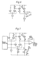
- the present invention provides a charge pump circuit comprising an operational amplifier having a first input and a second input and an output, a feedback loop including reactance means coupled between the output and second input, a first current source providing a first current to a first resistance which is coupled to said first input, a second current source providing a second current equal to said first current, first npn transistor switch means for selectively switching said second current to said second input, a second resistance equal in value to said first resistance coupled to said second input and second npn transistor means for selectively switching a third current equal and opposite to said first current via said second resistance to said second input, whereby said reactance means is charge pumped by said second and third currents.
- An important feature of the invention is that said second and third currents are made equal to the first current, said third current being made equal by choosing a second resistance equal in value to the first resistance. Since the first and second resistances are coupled to inputs of an operational amplifier and are thus effectively coupled to a virtual earth node, it is ensured that the current flows are equal.
- said second current could be provided by a similar resistance arrangement, it is preferred to provide the second current by a current source coupled to the first current source by means of a current mirror technique.
- a bi-directional current source has been designed which uses only npn transistors and can therefore be fabricated on IC processes without pnp transistors.
Landscapes
- Stabilization Of Oscillater, Synchronisation, Frequency Synthesizers (AREA)
Applications Claiming Priority (2)
| Application Number | Priority Date | Filing Date | Title |
|---|---|---|---|
| GB9023671 | 1990-10-31 | ||
| GB9023671A GB2249443B (en) | 1990-10-31 | 1990-10-31 | Charge pump circuit |
Publications (3)
| Publication Number | Publication Date |
|---|---|
| EP0484059A2 true EP0484059A2 (fr) | 1992-05-06 |
| EP0484059A3 EP0484059A3 (en) | 1993-02-24 |
| EP0484059B1 EP0484059B1 (fr) | 1994-04-27 |
Family
ID=10684644
Family Applications (1)
| Application Number | Title | Priority Date | Filing Date |
|---|---|---|---|
| EP91309870A Expired - Lifetime EP0484059B1 (fr) | 1990-10-31 | 1991-10-25 | Circuit de charge et de décharge |
Country Status (4)
| Country | Link |
|---|---|
| US (1) | US5239455A (fr) |
| EP (1) | EP0484059B1 (fr) |
| DE (1) | DE69101824T2 (fr) |
| GB (1) | GB2249443B (fr) |
Cited By (9)
| Publication number | Priority date | Publication date | Assignee | Title |
|---|---|---|---|---|
| EP0614282A1 (fr) * | 1993-03-03 | 1994-09-07 | Philips Composants Et Semiconducteurs | Circuit de pompe de charge à faible consommation, faible bruit et synthétiseur de fréquence équipé d'un tel circuit |
| EP0608151A3 (fr) * | 1993-01-21 | 1995-04-19 | Gennum Corp | Circuit de pompe de charge à grande vitesse et peu de dérivé. |
| WO1997033365A1 (fr) * | 1996-03-05 | 1997-09-12 | Philips Electronics N.V. | Amplificateur operationnel |
| EP0803976A3 (fr) * | 1996-04-25 | 1997-11-05 | Plessey Semiconductors Limited | Amplificateur |
| WO2005057791A1 (fr) * | 2003-12-11 | 2005-06-23 | Mosaid Technologies Incorporated | Pompe de charge a impedance haute capacite pour boucle d'asservissement de phase /boucle d'asservissement de delai |
| US7532050B2 (en) | 2005-02-03 | 2009-05-12 | Mosaid Technologies, Inc. | Delay locked loop circuit and method |
| US7567133B2 (en) | 2006-04-06 | 2009-07-28 | Mosaid Technologies Corporation | Phase-locked loop filter capacitance with a drag current |
| US7642836B2 (en) | 2004-07-09 | 2010-01-05 | Mosaid Technologies Incorporated | Systems and methods for minimizing static leakage of an integrated circuit |
| US7750695B2 (en) | 2004-12-13 | 2010-07-06 | Mosaid Technologies Incorporated | Phase-locked loop circuitry using charge pumps with current mirror circuitry |
Families Citing this family (14)
| Publication number | Priority date | Publication date | Assignee | Title |
|---|---|---|---|---|
| US5428626A (en) * | 1993-10-18 | 1995-06-27 | Tektronix, Inc. | Timing analyzer for embedded testing |
| US5453680A (en) * | 1994-01-28 | 1995-09-26 | Texas Instruments Incorporated | Charge pump circuit and method |
| US5422603A (en) * | 1994-06-02 | 1995-06-06 | International Business Machines Corporation | CMOS frequency synthesizer |
| KR100307514B1 (ko) * | 1994-07-30 | 2001-12-01 | 김영환 | 차지펌프회로 |
| US5592370A (en) * | 1994-09-19 | 1997-01-07 | Sun Microsystems, Inc. | Regulated complementary charge pump circuit |
| EP0772283B1 (fr) * | 1995-10-31 | 2000-01-12 | STMicroelectronics S.r.l. | Multiplicateur de tension avec régulation lineaire |
| GB2312578B (en) * | 1996-04-25 | 2000-07-05 | Plessey Semiconductors Ltd | Phase-locked loops |
| US5841324A (en) * | 1996-06-20 | 1998-11-24 | Harris Corporation | Charge-based frequency locked loop and method |
| US5781036A (en) * | 1997-04-01 | 1998-07-14 | Maxim Integrated Products, Inc. | Phase detector |
| US6124755A (en) * | 1997-09-29 | 2000-09-26 | Intel Corporation | Method and apparatus for biasing a charge pump |
| US6075406A (en) * | 1998-06-16 | 2000-06-13 | Macronix International Ltd. | High speed differential charge pump apparatus and method using a replica circuit to control common mode output voltage |
| JP3621588B2 (ja) * | 1998-09-28 | 2005-02-16 | 東芝情報システム株式会社 | チャージポンプ回路 |
| US6229345B1 (en) | 1999-09-15 | 2001-05-08 | Cypress Semiconductor Corp. | High speed charge-pump |
| US7777541B1 (en) | 2006-02-01 | 2010-08-17 | Cypress Semiconductor Corporation | Charge pump circuit and method for phase locked loop |
Family Cites Families (4)
| Publication number | Priority date | Publication date | Assignee | Title |
|---|---|---|---|---|
| US4636748A (en) * | 1985-06-26 | 1987-01-13 | Data General Corporation | Charge pump for use in a phase-locked loop |
| AU591496B2 (en) * | 1985-06-26 | 1989-12-07 | Data General Corporation | A charge pump for use in a phase-locked loop |
| US4829391A (en) * | 1987-08-04 | 1989-05-09 | Micropolis Corporation | High speed integrated charge pump circuit for phase lock loops |
| US4959618A (en) * | 1989-02-16 | 1990-09-25 | Vtc Incorporated | Differential charge pump for a phase locked loop |
-
1990
- 1990-10-31 GB GB9023671A patent/GB2249443B/en not_active Expired - Lifetime
-
1991
- 1991-10-17 US US07/777,804 patent/US5239455A/en not_active Expired - Fee Related
- 1991-10-25 EP EP91309870A patent/EP0484059B1/fr not_active Expired - Lifetime
- 1991-10-25 DE DE69101824T patent/DE69101824T2/de not_active Expired - Fee Related
Cited By (26)
| Publication number | Priority date | Publication date | Assignee | Title |
|---|---|---|---|---|
| EP0608151A3 (fr) * | 1993-01-21 | 1995-04-19 | Gennum Corp | Circuit de pompe de charge à grande vitesse et peu de dérivé. |
| EP0614282A1 (fr) * | 1993-03-03 | 1994-09-07 | Philips Composants Et Semiconducteurs | Circuit de pompe de charge à faible consommation, faible bruit et synthétiseur de fréquence équipé d'un tel circuit |
| FR2702317A1 (fr) * | 1993-03-03 | 1994-09-09 | Philips Composants | Circuit pompe de charge à faible consommation, faible bruit et synthétiseur de fréquence équipé d'un tel circuit. |
| WO1997033365A1 (fr) * | 1996-03-05 | 1997-09-12 | Philips Electronics N.V. | Amplificateur operationnel |
| EP0803976A3 (fr) * | 1996-04-25 | 1997-11-05 | Plessey Semiconductors Limited | Amplificateur |
| US7692461B2 (en) | 2003-12-11 | 2010-04-06 | Mosaid Technologies Incorporated | Charge pump for PLL/DLL |
| US7893737B2 (en) | 2003-12-11 | 2011-02-22 | Mosaid Technologies Incorporated | Charge pump for PLL/DLL |
| US7408391B2 (en) | 2003-12-11 | 2008-08-05 | Mosaid Technologies, Inc. | Charge pump for PLL/DLL |
| USRE49018E1 (en) | 2003-12-11 | 2022-04-05 | Mosaid Technologies Incorporated | Charge pump for PLL/DLL |
| USRE47715E1 (en) | 2003-12-11 | 2019-11-05 | Conversant Intellectual Property Management Inc. | Charge pump for PLL/DLL |
| US7616035B2 (en) | 2003-12-11 | 2009-11-10 | Mosaid Technologies, Inc. | Charge pump for PLL/DLL |
| US8222937B2 (en) | 2003-12-11 | 2012-07-17 | Mosaid Technologies Incorporated | Charge pump for PLL/DLL |
| WO2005057791A1 (fr) * | 2003-12-11 | 2005-06-23 | Mosaid Technologies Incorporated | Pompe de charge a impedance haute capacite pour boucle d'asservissement de phase /boucle d'asservissement de delai |
| US8049541B2 (en) | 2003-12-11 | 2011-11-01 | Mosaid Technologies Incorporated | Charge pump for PLL/DLL |
| US7176733B2 (en) | 2003-12-11 | 2007-02-13 | Mosaid Technologies, Inc. | High output impedance charge pump for PLL/DLL |
| US7982532B2 (en) | 2004-07-09 | 2011-07-19 | Mosaid Technologies Incorporated | Systems and methods for minimizing static leakage of an integrated circuit |
| US8134406B2 (en) | 2004-07-09 | 2012-03-13 | Mosaid Technologies Incorporated | Systems and methods for minimizing static leakage of an integrated circuit |
| US7642836B2 (en) | 2004-07-09 | 2010-01-05 | Mosaid Technologies Incorporated | Systems and methods for minimizing static leakage of an integrated circuit |
| USRE48410E1 (en) | 2004-07-09 | 2021-01-26 | Conversant Intellectual Property Management Inc. | Systems and methods for minimizing static leakage of an integrated circuit |
| USRE49854E1 (en) | 2004-07-09 | 2024-02-27 | Mosaid Technologies Incorporated | Systems and methods for minimizing static leakage of an integrated circuit |
| US7868808B2 (en) | 2004-12-13 | 2011-01-11 | Mosaid Technologies Incorporated | Phase-locked loop circuitry using charge pumps with current mirror circuitry |
| US7750695B2 (en) | 2004-12-13 | 2010-07-06 | Mosaid Technologies Incorporated | Phase-locked loop circuitry using charge pumps with current mirror circuitry |
| USRE43947E1 (en) | 2005-02-03 | 2013-01-29 | Mosaid Technologies Incorporated | Delay locked loop circuit and method |
| US8704569B2 (en) | 2005-02-03 | 2014-04-22 | Mosaid Technologies Incorporated | Delay locked loop circuit and method |
| US7532050B2 (en) | 2005-02-03 | 2009-05-12 | Mosaid Technologies, Inc. | Delay locked loop circuit and method |
| US7567133B2 (en) | 2006-04-06 | 2009-07-28 | Mosaid Technologies Corporation | Phase-locked loop filter capacitance with a drag current |
Also Published As
| Publication number | Publication date |
|---|---|
| DE69101824T2 (de) | 1994-08-11 |
| GB9023671D0 (en) | 1990-12-12 |
| EP0484059B1 (fr) | 1994-04-27 |
| EP0484059A3 (en) | 1993-02-24 |
| GB2249443A (en) | 1992-05-06 |
| US5239455A (en) | 1993-08-24 |
| GB2249443B (en) | 1994-06-08 |
| DE69101824D1 (de) | 1994-06-01 |
Similar Documents
| Publication | Publication Date | Title |
|---|---|---|
| EP0484059A2 (fr) | Circuit de charge et de décharge | |
| KR970003096B1 (ko) | 고속 고정 전류 감소 및 클램핑 회로를 구비한 위상 고정 루프 | |
| EP0529836A1 (fr) | Détecteur intégrant de phase | |
| EP0379955A1 (fr) | Circuit ECL et son utilisation en connexion avec un oscillateur contrôlé par voltage | |
| US4659949A (en) | Phase-locked loop circuit | |
| EP0608151B1 (fr) | Circuit de pompe de charge à grande vitesse et peu de dérivé | |
| EP0730345B1 (fr) | Circuit à gain variable | |
| US4691120A (en) | Pulse delay circuit device | |
| US5416691A (en) | Charge pump circuit | |
| US3922602A (en) | Lock detector for a phase locked loop | |
| US4468636A (en) | Low temperature coefficient wide band-width voltage controlled oscillator | |
| US5543742A (en) | Phase shifting circuit | |
| US5103123A (en) | Phase detector having all NPN transistors | |
| US4499386A (en) | Trigger circuit | |
| US4791325A (en) | Class B clamp circuit | |
| EP0647027B1 (fr) | Commutateur précis du courant à basse tension | |
| EP0377978B1 (fr) | Appareil de commande pour un circuit PLL | |
| US6466097B1 (en) | Phase locked loop and associated control method | |
| US6618448B1 (en) | DC recovery circuit capable of receiving ECL signal even under low power supply voltage | |
| US4945415A (en) | Slew enhancement circuit for an automatic frequency control system | |
| KR100244517B1 (ko) | 페이즈 록 루프의 입력 버퍼 | |
| JPH05191276A (ja) | 位相検出器 | |
| JP2000224034A (ja) | Pll回路 | |
| JPS5938761Y2 (ja) | Pll回路のロ−パスフィルタ | |
| EP0255826B1 (fr) | Charge differentielle equilibree |
Legal Events
| Date | Code | Title | Description |
|---|---|---|---|
| PUAI | Public reference made under article 153(3) epc to a published international application that has entered the european phase |
Free format text: ORIGINAL CODE: 0009012 |
|
| AK | Designated contracting states |
Kind code of ref document: A2 Designated state(s): DE FR IT |
|
| RAP1 | Party data changed (applicant data changed or rights of an application transferred) |
Owner name: PLESSEY SEMICONDUCTORS LIMITED |
|
| PUAL | Search report despatched |
Free format text: ORIGINAL CODE: 0009013 |
|
| AK | Designated contracting states |
Kind code of ref document: A3 Designated state(s): DE FR IT |
|
| 17P | Request for examination filed |
Effective date: 19930311 |
|
| 17Q | First examination report despatched |
Effective date: 19930623 |
|
| GRAA | (expected) grant |
Free format text: ORIGINAL CODE: 0009210 |
|
| AK | Designated contracting states |
Kind code of ref document: B1 Designated state(s): DE FR IT |
|
| ITF | It: translation for a ep patent filed | ||
| ET | Fr: translation filed | ||
| REF | Corresponds to: |
Ref document number: 69101824 Country of ref document: DE Date of ref document: 19940601 |
|
| PLBE | No opposition filed within time limit |
Free format text: ORIGINAL CODE: 0009261 |
|
| STAA | Information on the status of an ep patent application or granted ep patent |
Free format text: STATUS: NO OPPOSITION FILED WITHIN TIME LIMIT |
|
| 26N | No opposition filed | ||
| REG | Reference to a national code |
Ref country code: FR Ref legal event code: CD |
|
| REG | Reference to a national code |
Ref country code: FR Ref legal event code: CD |
|
| PGFP | Annual fee paid to national office [announced via postgrant information from national office to epo] |
Ref country code: FR Payment date: 20031003 Year of fee payment: 13 |
|
| PGFP | Annual fee paid to national office [announced via postgrant information from national office to epo] |
Ref country code: DE Payment date: 20031103 Year of fee payment: 13 |
|
| PG25 | Lapsed in a contracting state [announced via postgrant information from national office to epo] |
Ref country code: DE Free format text: LAPSE BECAUSE OF NON-PAYMENT OF DUE FEES Effective date: 20050503 |
|
| PG25 | Lapsed in a contracting state [announced via postgrant information from national office to epo] |
Ref country code: FR Free format text: LAPSE BECAUSE OF NON-PAYMENT OF DUE FEES Effective date: 20050630 |
|
| REG | Reference to a national code |
Ref country code: FR Ref legal event code: ST |
|
| PG25 | Lapsed in a contracting state [announced via postgrant information from national office to epo] |
Ref country code: IT Free format text: LAPSE BECAUSE OF NON-PAYMENT OF DUE FEES;WARNING: LAPSES OF ITALIAN PATENTS WITH EFFECTIVE DATE BEFORE 2007 MAY HAVE OCCURRED AT ANY TIME BEFORE 2007. THE CORRECT EFFECTIVE DATE MAY BE DIFFERENT FROM THE ONE RECORDED. Effective date: 20051025 |