EP0485216B1 - Afficheur en couleurs à cristal liquide - Google Patents
Afficheur en couleurs à cristal liquide Download PDFInfo
- Publication number
- EP0485216B1 EP0485216B1 EP91310319A EP91310319A EP0485216B1 EP 0485216 B1 EP0485216 B1 EP 0485216B1 EP 91310319 A EP91310319 A EP 91310319A EP 91310319 A EP91310319 A EP 91310319A EP 0485216 B1 EP0485216 B1 EP 0485216B1
- Authority
- EP
- European Patent Office
- Prior art keywords
- display
- colour
- liquid crystal
- electrodes
- crystal display
- Prior art date
- Legal status (The legal status is an assumption and is not a legal conclusion. Google has not performed a legal analysis and makes no representation as to the accuracy of the status listed.)
- Expired - Lifetime
Links
Images

Classifications
-
- G—PHYSICS
- G02—OPTICS
- G02F—OPTICAL DEVICES OR ARRANGEMENTS FOR THE CONTROL OF LIGHT BY MODIFICATION OF THE OPTICAL PROPERTIES OF THE MEDIA OF THE ELEMENTS INVOLVED THEREIN; NON-LINEAR OPTICS; FREQUENCY-CHANGING OF LIGHT; OPTICAL LOGIC ELEMENTS; OPTICAL ANALOGUE/DIGITAL CONVERTERS
- G02F1/00—Devices or arrangements for the control of the intensity, colour, phase, polarisation or direction of light arriving from an independent light source, e.g. switching, gating or modulating; Non-linear optics
- G02F1/01—Devices or arrangements for the control of the intensity, colour, phase, polarisation or direction of light arriving from an independent light source, e.g. switching, gating or modulating; Non-linear optics for the control of the intensity, phase, polarisation or colour
- G02F1/13—Devices or arrangements for the control of the intensity, colour, phase, polarisation or direction of light arriving from an independent light source, e.g. switching, gating or modulating; Non-linear optics for the control of the intensity, phase, polarisation or colour based on liquid crystals, e.g. single liquid crystal display cells
- G02F1/133—Constructional arrangements; Operation of liquid crystal cells; Circuit arrangements
- G02F1/1333—Constructional arrangements; Manufacturing methods
- G02F1/1343—Electrodes
- G02F1/134309—Electrodes characterised by their geometrical arrangement
- G02F1/134327—Segmented, e.g. alpha numeric display
-
- G—PHYSICS
- G02—OPTICS
- G02F—OPTICAL DEVICES OR ARRANGEMENTS FOR THE CONTROL OF LIGHT BY MODIFICATION OF THE OPTICAL PROPERTIES OF THE MEDIA OF THE ELEMENTS INVOLVED THEREIN; NON-LINEAR OPTICS; FREQUENCY-CHANGING OF LIGHT; OPTICAL LOGIC ELEMENTS; OPTICAL ANALOGUE/DIGITAL CONVERTERS
- G02F1/00—Devices or arrangements for the control of the intensity, colour, phase, polarisation or direction of light arriving from an independent light source, e.g. switching, gating or modulating; Non-linear optics
- G02F1/01—Devices or arrangements for the control of the intensity, colour, phase, polarisation or direction of light arriving from an independent light source, e.g. switching, gating or modulating; Non-linear optics for the control of the intensity, phase, polarisation or colour
- G02F1/13—Devices or arrangements for the control of the intensity, colour, phase, polarisation or direction of light arriving from an independent light source, e.g. switching, gating or modulating; Non-linear optics for the control of the intensity, phase, polarisation or colour based on liquid crystals, e.g. single liquid crystal display cells
- G02F1/133—Constructional arrangements; Operation of liquid crystal cells; Circuit arrangements
- G02F1/1333—Constructional arrangements; Manufacturing methods
- G02F1/1335—Structural association of cells with optical devices, e.g. polarisers or reflectors
- G02F1/133509—Filters, e.g. light shielding masks
- G02F1/133514—Colour filters
Definitions
- the present invention relates to a colour liquid crystal display.
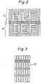
- a colour liquid crystal display in which, as shown in Fig.4, display patterns are formed by portions where transparent comb electrodes 21 and 22 on the SEG (segment) side, serving as display electrodes, overlap transparent electrodes 23 and 24 on the COM (common) side, respectively.
- Each element of the SEG-side display electrode 21 faces a red color filter (not shown), while each element of SEG-side display electrode 22 faces a green color filter (not shown).
- the display patterns are independent, the comb electrodes being individually connected to different signal lines.
- the display area C where display patterns are defined by the SEG-side display electrode 21 is separated from the display area D where display patterns are defined by the SEG-side display electrode 22, and the display areas C and D cannot be brought in contact with each other or made to overlap. It is therefore not possible to make a plurality of display patterns overlap each other within one display area, the resulting problem being an inability to further increase the number of display patterns per unit display area.
- a colour liquid crystal display comprises:
- the display electrodes disposed adjacent to each other are formed extending into each other's display area in alternating fashion, display patterns formed by the adjacent display electrodes are made to overlap each other within one display area. Therefore, the number of display patterns per unit display area can be increased.
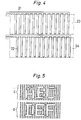
- the SEG-side transparent comb electrodes 1 and 2 are arranged extending into each other's area in alternating fashion. Also, the SEG-side transparent electrodes 1 and 2 share a COM-side electrode 3 disposed opposite them across the liquid crystal layer (not shown) and form two different display patterns, upper and lower, respectively driven independently of each other.
- a mask 6 which serves as a light-blocking member formed extending between the colour filters R, G, B.
- production of the above display patterns is achieved by applying varying voltages to the SEG-side transparent comb electrodes 1, 2 and the COM-Side electrode 3 and thereby varying the molecular alignment in the liquid crystal layer.
- overlapping portions 5 are formed where the display area defined by the SEG-side transparent electrode 1 overlaps the display area defined by the SEG-side transparent electrode 2. That is, in the colour liquid crystal display of this embodiment, since the display area A, where the red display pattern defined by the SEG-side transparent electrode 1 is formed, overlaps the display area B where the green display area defined by the SEG-side transparent electrode 2 is formed, the number of display patterns per unit display area can be increased.
Landscapes
- Physics & Mathematics (AREA)
- Nonlinear Science (AREA)
- Mathematical Physics (AREA)
- Chemical & Material Sciences (AREA)
- Crystallography & Structural Chemistry (AREA)
- General Physics & Mathematics (AREA)
- Optics & Photonics (AREA)
- Geometry (AREA)
- Liquid Crystal (AREA)
Claims (5)
- Dispositif d'affichage en couleurs à cristaux liquides comportant:une pluralité d'éléments de sélection de couleur (R, V, B), pour transmettre respectivement une lumière de couleur spécifique, s'étendant sur tout un secteur d'affichage du dispositif;des premières électrodes d'affichage (1) définissant un premier motif d'image prédéterminé à afficher dans une première zone d'affichage dudit secteur, lesdites premières électrodes d'affichage étant en correspondance avec ceux des éléments de sélection de couleur qui sélectionnent une première couleur; etdes secondes électrodes d'affichage (2) définissant un second motif d'image prédéterminé à afficher dans une seconde zone d'affichage dudit secteur, lesdites secondes électrodes d'affichage étant en correspondance avec ceux des éléments de sélection de couleur qui sélectionnent une seconde couleur;dans lequel lesdites première et seconde zones d'affichage se recouvrent seulement partiellement dans une zone frontière (5) dans laquelle des parties des premières et secondes électrodes d'affichage sont disposées de façon à s'étendre dans les zones d'affichage les unes des autres de manière alternée.
- Dispositif d'affichage en couleurs à cristaux liquides selon la revendication 1, dans lequel les premières et secondes électrodes d'affichage (1, 2) ont la forme d'un peigne dont les extrémités des dents sont intercalées dans ladite zone frontière (5).
- Dispositif d'affichage en couleurs à cristaux liquides selon la revendication 1 ou 2, dans lequel les premières et secondes électrodes d'affichage (1, 2) sont placées face à la même électrode masse (3).
- Dispositif d'affichage en couleurs à cristaux liquides selon l'une quelconque des revendications 1 à 3, dans lequel un élément formant écran à la lumière (6) est interposé entre les éléments de sélection de couleur adjacents.
- Dispositif d'affichage en couleurs à cristaux liquides selon l'une quelconque des revendications 1 à 4, dans lequel les éléments de sélection de couleur sont des filtres de couleurs sélectionnant trois couleurs, le rouge (R), le vert (V) et le bleu (B).
Applications Claiming Priority (2)
| Application Number | Priority Date | Filing Date | Title |
|---|---|---|---|
| JP303077/90 | 1990-11-07 | ||
| JP2303077A JPH04174417A (ja) | 1990-11-07 | 1990-11-07 | カラー液晶表示装置 |
Publications (3)
| Publication Number | Publication Date |
|---|---|
| EP0485216A2 EP0485216A2 (fr) | 1992-05-13 |
| EP0485216A3 EP0485216A3 (en) | 1992-10-07 |
| EP0485216B1 true EP0485216B1 (fr) | 1996-02-07 |
Family
ID=17916620
Family Applications (1)
| Application Number | Title | Priority Date | Filing Date |
|---|---|---|---|
| EP91310319A Expired - Lifetime EP0485216B1 (fr) | 1990-11-07 | 1991-11-07 | Afficheur en couleurs à cristal liquide |
Country Status (4)
| Country | Link |
|---|---|
| US (1) | US5233449A (fr) |
| EP (1) | EP0485216B1 (fr) |
| JP (1) | JPH04174417A (fr) |
| DE (1) | DE69116983T2 (fr) |
Families Citing this family (16)
| Publication number | Priority date | Publication date | Assignee | Title |
|---|---|---|---|---|
| US5434690A (en) * | 1993-07-27 | 1995-07-18 | Kabushiki Kaisha Toshiba | Liquid crystal device with pixel electrodes in an opposed striped form |
| FR2712109B1 (fr) * | 1993-11-04 | 1995-12-15 | Ebauchesfabrik Eta Ag | Dispositif d'affichage à cristaux liquides. |
| KR100304912B1 (ko) * | 1993-12-30 | 2002-08-24 | 엘지.필립스 엘시디 주식회사 | 액정표시소자의구조및구동방법 |
| JPH10325961A (ja) * | 1994-03-17 | 1998-12-08 | Hitachi Ltd | アクティブマトリクス型液晶表示装置 |
| US5420052A (en) * | 1994-04-19 | 1995-05-30 | Texas Instruments Incorporated | Method of fabricating a semiplanar heterojunction bipolar transistor |
| JP3529460B2 (ja) * | 1994-12-01 | 2004-05-24 | 株式会社東芝 | 液晶表示装置 |
| TW329500B (en) | 1995-11-14 | 1998-04-11 | Handotai Energy Kenkyusho Kk | Electro-optical device |
| JPH09146108A (ja) * | 1995-11-17 | 1997-06-06 | Semiconductor Energy Lab Co Ltd | 液晶表示装置およびその駆動方法 |
| JP2776376B2 (ja) * | 1996-06-21 | 1998-07-16 | 日本電気株式会社 | アクティブマトリクス液晶表示パネル |
| KR100250796B1 (ko) * | 1996-11-29 | 2000-04-01 | 김영환 | 액정 표시 소자 및 그 제조방법 |
| JPH10186366A (ja) * | 1996-12-26 | 1998-07-14 | Fujitsu Ltd | 液晶表示装置 |
| US6704083B1 (en) * | 1997-05-30 | 2004-03-09 | Samsung Electronics, Co., Ltd. | Liquid crystal display including polarizing plate having polarizing directions neither parallel nor perpendicular to average alignment direction of molecules |
| TW434443B (en) | 1997-05-30 | 2001-05-16 | Samsung Electronics Co Ltd | Liquid crystal display |
| KR100293806B1 (ko) * | 1997-06-25 | 2001-10-24 | 박종섭 | 액정표시소자 |
| GB2327797A (en) * | 1997-07-31 | 1999-02-03 | Sharp Kk | Spatial light modulator and display |
| JP2014206639A (ja) * | 2013-04-12 | 2014-10-30 | 株式会社ジャパンディスプレイ | 液晶表示装置 |
Family Cites Families (10)
| Publication number | Priority date | Publication date | Assignee | Title |
|---|---|---|---|---|
| US3820875A (en) * | 1972-04-14 | 1974-06-28 | W Bohmer | Scanner devices utilizing field effect light scattering dielectrics |
| JPS55134885A (en) * | 1979-04-06 | 1980-10-21 | Stanley Electric Co Ltd | Liquid crystal display device |
| JPS59136718A (ja) * | 1983-01-26 | 1984-08-06 | Mitsubishi Electric Corp | 液晶表示素子 |
| KR910007013B1 (ko) * | 1985-10-09 | 1991-09-14 | 가부시기가이샤 히다찌세이사꾸쇼 | 컬러액정표시소자 |
| JPS6370828A (ja) * | 1986-09-12 | 1988-03-31 | Matsushita Electric Ind Co Ltd | マトリクス型液晶表示装置およびその製造方法 |
| JPH0748259B2 (ja) * | 1987-06-24 | 1995-05-24 | 松下電器産業株式会社 | 光学式ディスク記録再生装置 |
| JPS6436120A (en) * | 1987-07-30 | 1989-02-07 | Nec Corp | Redundant constitution gate array |
| JPS6442633A (en) * | 1987-08-10 | 1989-02-14 | Koito Mfg Co Ltd | Liquid crystal display device for color display |
| JP2594985B2 (ja) * | 1987-11-24 | 1997-03-26 | 株式会社日立製作所 | 液晶表示素子 |
| EP0434220B1 (fr) * | 1989-11-20 | 1996-04-10 | Sharp Kabushiki Kaisha | Dispositif d'affichage en couleurs à cristal liquide |
-
1990
- 1990-11-07 JP JP2303077A patent/JPH04174417A/ja active Pending
-
1991
- 1991-11-04 US US07/787,020 patent/US5233449A/en not_active Expired - Lifetime
- 1991-11-07 DE DE69116983T patent/DE69116983T2/de not_active Expired - Fee Related
- 1991-11-07 EP EP91310319A patent/EP0485216B1/fr not_active Expired - Lifetime
Also Published As
| Publication number | Publication date |
|---|---|
| DE69116983T2 (de) | 1996-07-18 |
| US5233449A (en) | 1993-08-03 |
| EP0485216A2 (fr) | 1992-05-13 |
| JPH04174417A (ja) | 1992-06-22 |
| EP0485216A3 (en) | 1992-10-07 |
| DE69116983D1 (de) | 1996-03-21 |
Similar Documents
| Publication | Publication Date | Title |
|---|---|---|
| EP0485216B1 (fr) | Afficheur en couleurs à cristal liquide | |
| US4902103A (en) | Color liquid-crystal display unit with electrodes interleaved in vertical and horizontal directions | |
| EP0302653B1 (fr) | Ecran coloré | |
| KR970016724A (ko) | 오버랩하는 컬러 필터를 갖는 액정 디스플레이 장치 | |
| JPH0341416A (ja) | カラー液晶シャッターマトリクス | |
| CN108398826A (zh) | 异形显示面板及显示装置 | |
| JPH07114018A (ja) | カラー液晶表示装置 | |
| EP0219064B1 (fr) | Dispositif d'affichage à cristal liquide en couleurs | |
| JPH06160910A (ja) | 表示デバイス | |
| JP3536447B2 (ja) | カラー液晶表示素子 | |
| EP0317850A2 (fr) | Dispositif d'affichage à cristal liquide | |
| JPS5885418A (ja) | 受動型マルチカラ−表示装置 | |
| JPH0561035A (ja) | 液晶表示装置 | |
| JPS6283721A (ja) | カラ−液晶表示素子 | |
| JPS6291917A (ja) | 液晶表示装置 | |
| JPS6259924A (ja) | マトリクス型液晶表示装置 | |
| JP2000352721A (ja) | 液晶表示装置 | |
| JPS60260921A (ja) | 液晶表示装置 | |
| JP3850584B2 (ja) | バックライト式部分カラー液晶表示装置の構造 | |
| JPH0643779Y2 (ja) | 液晶表示素子 | |
| JPH0350493Y2 (fr) | ||
| JPH0821995A (ja) | カラー液晶表示装置およびその製造方法 | |
| JPH0641213Y2 (ja) | カラー液晶表示素子 | |
| JPH0244314A (ja) | カラー液晶パネルの支持基板 | |
| JPS63187218A (ja) | カラ−表示液晶表示装置 |
Legal Events
| Date | Code | Title | Description |
|---|---|---|---|
| PUAI | Public reference made under article 153(3) epc to a published international application that has entered the european phase |
Free format text: ORIGINAL CODE: 0009012 |
|
| AK | Designated contracting states |
Kind code of ref document: A2 Designated state(s): DE FR GB |
|
| PUAL | Search report despatched |
Free format text: ORIGINAL CODE: 0009013 |
|
| AK | Designated contracting states |
Kind code of ref document: A3 Designated state(s): DE FR GB |
|
| 17P | Request for examination filed |
Effective date: 19921215 |
|
| 17Q | First examination report despatched |
Effective date: 19940531 |
|
| GRAA | (expected) grant |
Free format text: ORIGINAL CODE: 0009210 |
|
| AK | Designated contracting states |
Kind code of ref document: B1 Designated state(s): DE FR GB |
|
| REF | Corresponds to: |
Ref document number: 69116983 Country of ref document: DE Date of ref document: 19960321 |
|
| ET | Fr: translation filed | ||
| PLBE | No opposition filed within time limit |
Free format text: ORIGINAL CODE: 0009261 |
|
| STAA | Information on the status of an ep patent application or granted ep patent |
Free format text: STATUS: NO OPPOSITION FILED WITHIN TIME LIMIT |
|
| 26N | No opposition filed | ||
| PGFP | Annual fee paid to national office [announced via postgrant information from national office to epo] |
Ref country code: GB Payment date: 20011107 Year of fee payment: 11 |
|
| PGFP | Annual fee paid to national office [announced via postgrant information from national office to epo] |
Ref country code: FR Payment date: 20011113 Year of fee payment: 11 |
|
| PGFP | Annual fee paid to national office [announced via postgrant information from national office to epo] |
Ref country code: DE Payment date: 20011119 Year of fee payment: 11 |
|
| REG | Reference to a national code |
Ref country code: GB Ref legal event code: IF02 |
|
| PG25 | Lapsed in a contracting state [announced via postgrant information from national office to epo] |
Ref country code: GB Free format text: LAPSE BECAUSE OF NON-PAYMENT OF DUE FEES Effective date: 20021107 |
|
| PG25 | Lapsed in a contracting state [announced via postgrant information from national office to epo] |
Ref country code: DE Free format text: LAPSE BECAUSE OF NON-PAYMENT OF DUE FEES Effective date: 20030603 |
|
| GBPC | Gb: european patent ceased through non-payment of renewal fee | ||
| PG25 | Lapsed in a contracting state [announced via postgrant information from national office to epo] |
Ref country code: FR Free format text: LAPSE BECAUSE OF NON-PAYMENT OF DUE FEES Effective date: 20030731 |
|
| REG | Reference to a national code |
Ref country code: FR Ref legal event code: ST |