EP0485435B1 - Module pour un systeme reflechissant de modulation de lumiere - Google Patents
Module pour un systeme reflechissant de modulation de lumiere Download PDFInfo
- Publication number
- EP0485435B1 EP0485435B1 EP90911541A EP90911541A EP0485435B1 EP 0485435 B1 EP0485435 B1 EP 0485435B1 EP 90911541 A EP90911541 A EP 90911541A EP 90911541 A EP90911541 A EP 90911541A EP 0485435 B1 EP0485435 B1 EP 0485435B1
- Authority
- EP
- European Patent Office
- Prior art keywords
- light
- active matrix
- image plane
- wafer
- reflective image
- Prior art date
- Legal status (The legal status is an assumption and is not a legal conclusion. Google has not performed a legal analysis and makes no representation as to the accuracy of the status listed.)
- Revoked
Links
- 239000011159 matrix material Substances 0.000 claims abstract description 37
- 238000003384 imaging method Methods 0.000 claims abstract description 15
- 239000000463 material Substances 0.000 claims description 23
- 239000000758 substrate Substances 0.000 claims description 13
- 239000013078 crystal Substances 0.000 claims description 4
- 239000007787 solid Substances 0.000 claims description 3
- 235000012431 wafers Nutrition 0.000 description 30
- 239000004973 liquid crystal related substance Substances 0.000 description 15
- 229910021417 amorphous silicon Inorganic materials 0.000 description 6
- 229910021420 polycrystalline silicon Inorganic materials 0.000 description 5
- 230000007423 decrease Effects 0.000 description 4
- 239000000835 fiber Substances 0.000 description 3
- 239000011521 glass Substances 0.000 description 3
- VYPSYNLAJGMNEJ-UHFFFAOYSA-N Silicium dioxide Chemical compound O=[Si]=O VYPSYNLAJGMNEJ-UHFFFAOYSA-N 0.000 description 2
- 238000011960 computer-aided design Methods 0.000 description 2
- 239000005350 fused silica glass Substances 0.000 description 2
- 238000004519 manufacturing process Methods 0.000 description 2
- 229920005591 polysilicon Polymers 0.000 description 2
- 239000010409 thin film Substances 0.000 description 2
- XUIMIQQOPSSXEZ-UHFFFAOYSA-N Silicon Chemical compound [Si] XUIMIQQOPSSXEZ-UHFFFAOYSA-N 0.000 description 1
- 229910052782 aluminium Inorganic materials 0.000 description 1
- XAGFODPZIPBFFR-UHFFFAOYSA-N aluminium Chemical compound [Al] XAGFODPZIPBFFR-UHFFFAOYSA-N 0.000 description 1
- 239000002131 composite material Substances 0.000 description 1
- 238000010276 construction Methods 0.000 description 1
- 230000003247 decreasing effect Effects 0.000 description 1
- 230000002939 deleterious effect Effects 0.000 description 1
- 238000013461 design Methods 0.000 description 1
- 238000011161 development Methods 0.000 description 1
- 238000005516 engineering process Methods 0.000 description 1
- 229910052736 halogen Inorganic materials 0.000 description 1
- 238000002347 injection Methods 0.000 description 1
- 239000007924 injection Substances 0.000 description 1
- 230000010354 integration Effects 0.000 description 1
- 229910052751 metal Inorganic materials 0.000 description 1
- 239000002184 metal Substances 0.000 description 1
- 229910001507 metal halide Inorganic materials 0.000 description 1
- 238000000034 method Methods 0.000 description 1
- 238000012986 modification Methods 0.000 description 1
- 230000004048 modification Effects 0.000 description 1
- 229910021421 monocrystalline silicon Inorganic materials 0.000 description 1
- 230000003287 optical effect Effects 0.000 description 1
- 238000000206 photolithography Methods 0.000 description 1
- 229910052710 silicon Inorganic materials 0.000 description 1
- 239000010703 silicon Substances 0.000 description 1
- 239000011343 solid material Substances 0.000 description 1
- 230000000007 visual effect Effects 0.000 description 1
- 229910052724 xenon Inorganic materials 0.000 description 1
- -1 xenon metal halide Chemical class 0.000 description 1
Images



Classifications
-
- H—ELECTRICITY
- H04—ELECTRIC COMMUNICATION TECHNIQUE
- H04N—PICTORIAL COMMUNICATION, e.g. TELEVISION
- H04N9/00—Details of colour television systems
- H04N9/12—Picture reproducers
- H04N9/31—Projection devices for colour picture display, e.g. using electronic spatial light modulators [ESLM]
- H04N9/3141—Constructional details thereof
- H04N9/315—Modulator illumination systems
-
- G—PHYSICS
- G03—PHOTOGRAPHY; CINEMATOGRAPHY; ANALOGOUS TECHNIQUES USING WAVES OTHER THAN OPTICAL WAVES; ELECTROGRAPHY; HOLOGRAPHY
- G03B—APPARATUS OR ARRANGEMENTS FOR TAKING PHOTOGRAPHS OR FOR PROJECTING OR VIEWING THEM; APPARATUS OR ARRANGEMENTS EMPLOYING ANALOGOUS TECHNIQUES USING WAVES OTHER THAN OPTICAL WAVES; ACCESSORIES THEREFOR
- G03B21/00—Projectors or projection-type viewers; Accessories therefor
- G03B21/005—Projectors using an electronic spatial light modulator but not peculiar thereto
- G03B21/006—Projectors using an electronic spatial light modulator but not peculiar thereto using LCD's
Definitions
- the invention relates generally to light encoding systems and more particularly to an active matrix reflective encoding system.
- AMLCD's The cost of AMLCD's is largely determined by the yield of useable devices, where the yield is the percentage of useable devices from the total produced. Yield of AMLCD's is in large part determined by the device design, manufacturing process tolerance and the display size. In general, the larger the display size, the lower the yield and hence higher the cost of the device.
- the AMLCD effort has concentrated on utilizing a matrix of nonlinear devices on a glass or fused silica substrate.
- the nonlinear devices allow individual control over each display picture element or "pixel" to provide superior optimal performance.
- the nonlinear devices generally are amorphous or polycrystalline silicon thin film transistors (TFT); however, thin film diodes (TFD) and metal-insulator-metal (MIM) devices also have been employed.
- a transparent substrate is considered necessary for these displays, because most liquid crystal (LC) materials require a polarizer at both the front and the back of the LCD device. Further, the conventional position on color displays is that they must be transmissive rather than reflective, because of the light losses inherent in the color reflective mode.
- LC liquid crystal
- Amorphous silicon TFT AMLCD's utilize inexpensive drawn glass.
- Polycrystalline silicon on the other hand, requires either very high temperature glass or fused silica substrates. Either of these substrates is prohibitively expensive in widths over eight inches.
- the inexpensive amorphous silicon AMLCD substrates are offset by the fact that these displays require separate address devices which result in several hundred interconnections to the display substrate.
- Polycrystalline silicon AMLCD's allow integration of the addressing circuitry on the substrate which reduces the number of interconnections to a very few.
- New markets have been recognized which include home theatre high definition TV, audio visual machines and high resolution large area computer aided design (CAD) stations. Each of these markets require very large, high resolution, full color and video speed imaging.
- Applicant has determined that the large area dictates projection systems, either front or rear projection, that the high resolution requires integrated drivers and that projection systems do not require either transparent substrates or large display sizes. Further, these markets all essentially utilize what can be considered light encoding devices. Other types of light encoding devices include wafer or printed circuit board mask sets.
- WO-A-8810545 illustrates a projector having a light source, two dichroic prisms each having two dichroic colour-splitting layers and which on three of their sides have three liquid crystal light valve arrangements associated with different components of the colour image.
- a reflective image plane module comprises reflective imaging means for forming a reflected light beam from light passed thereto and for imparting information onto said reflected light beam; and means for passing light to said reflective imaging means and for projecting said reflected light beam for viewing, characterised in that the reflective imaging means includes a wafer based active matrix and in that said wafer is a non light transmissive single crystal wafer substrate with said active matrix formed on one surface of said wafer.
- a reflective image plane module comprises reflective imaging means, and is characterised in that the reflective imaging means includes a wafer based active matrix for forming a reflected light beam from light passed thereto and for imparting information onto said reflected light beam; and in that the module further comprises means for passing light to said wafer based active matrix and for projecting said reflected light beam for viewing, said light passing and projecting means including a prism with a light receiving projection for directing light, said prism forming at least a portion of said projecting means.
- the reflective image plane module includes a wafer based active matrix mated to a light directing and projecting structure.
- a source of light is directed to the reflective image plane module wherein the wafer based active matrix imparts or encodes information onto a light beam reflected therefrom.
- the reflective image plane module light projecting structure projects the reflected beam for viewing or imaging, such as through one or more lens.
- the wafer based active matrix preferably includes a specular reflective back surface and an LC or similar characteristic material formed thereon which is electronically altered to impart or encode the information to the light beam reflected therefrom.
- the LC material preferably is a solid light modulating material having bodies of LC material suspended in the solid material.
- the reflective image plane module light directing and projecting structure is formed from a prism or mirror which passes the light or light component through a first surface to the wafer based active matrix mated to a second surface and which projects the reflected light from the first surface to be viewed or imaged.
- a light source 12 provides light to a lens or lens system 14, which directs the light to a transmissive LCD 16.
- a video or computer signal source (not illustrated) is coupled by a line 18 to a video drive circuit 20.
- the video drive circuit 20 operates on the signal coupled thereto and generates the required drive signals coupled over a line 22 to the LCD 16.
- the drive signals will be the audio, red video, blue video, green video, vertical sync, horizontal sync, reset and pixel clock signals.
- the drive signals cause the pixels of the LCD 16 to block or transmit light to impart or encode the required information onto the light transmitted through the LCD 16 to a lens or lens system 24 which projects the composite color picture onto the screen 26.
- a monochrome projection system would operate in the same manner with only one video light component, rather than the separate blue, green and red video signals.
- transmissive projection system has been developed by Seiko Epson Corp. and utilizes three separate LCD panels, one for each of the blue, green and red video signals. The signals then are combined by a dichroic prism prior to projecting onto the screen.
- These transmissive projection systems suffer from a number of problems.
- One significant problem is caused by the construction required by the LC material.
- the LCD panels include a polarizer on each side of the LC material, such as twisted nematic material and are utilized as a shutter to absorb the light not to be transmitted. Both the polarizers and the LC material absorb light which generates heat, which is deleterious to the LCD panel. Further, because of the two polarizers, and the LC material utilized, only about fifteen per cent or less of the light directed to the LCD panel is transmitted therethrough for projection to the screen. The devices exhibit low brightness, because of the amount of light absorbed.
- the resolution of the transmissive panels is not as great as that which could be achieved if crystalline based technology was utilized.
- the pixel density can be made greater by placing the pixel drain pads centered over row and column lines in crystalline devices. Amorphous silicon devices have to leave spaces between pixels for the row and column lines and hence cannot be packed as densely without seriously decreasing the yield.
- deposited amorphous silicon devices have a much greater number of LCD panel interconnects. This decreases reliability and increases cost. These devices are also designed as large area devices which again decreases yield and increases costs.
- FIG. 30 top, front and side views of a first embodiment of a reflective image plane module of the present invention is designated generally by the reference character 30.
- a light source 32 such as a bulb and a reflector, provides a source of light. The light is columnated by a lens 34 and condensed or focused by a lens 36 to the reflective image plane module 30.
- the reflective image plane module 30 includes a first mirrored wall 40 which has an aperture 42 through which the light passes and impinges on a back wall 44 of the reflective image plane module 30.
- the back wall 44 has attached thereto or is formed of a wafer based active matrix 46.
- the light has the information imparted to or encoded on it by the wafer based active matrix 46 as it is reflected from the wafer based active matrix 46.
- One specific example of the wafer based active matrix is further described in EP-A-0438565.
- the wafer based active matrix 46 is a wafer based active matrix having a specular reflective back surface to reflect light therefrom.
- the wafer based active matrix is covered by an LCD or similar characteristic material, such as an electrophoretic material.
- One preferable LCD material is a solid light modulating material having bodies of LC material suspended therein. Examples of such LCD materials are described in U.S. Patent US-A-4,435,067 and US-A-4,688,900, which are incorporated herein by reference. Other types of LC material also can be utilized, such as dyed phase change or guest-host material.
- the light reflected from the wafer based active matrix 46 is reflected by a mirror back surface 48 of the wall 40.
- the reflected light is directed to a projection lens 50, which lens or lens system can be a fixed or zoom type lens. If utilized in a projector system, the reflected light is projected by the lens 50 to be viewed, typically on a screen (not illustrated).
- the reflective image plane module 30 as described can be utilized as a monochrome projection system or can be combined as will be described hereinafter to form a unit of a full color projection system. If utilized as a mask or portion of a mask system, the lens 50 will be utilized to focus the mask image onto a substrate (not illustrated).
- the reflective image plane module 30 generally only includes the light directing and reflecting structures formed by the elements 40, 42, 44 (including the wafer based active matrix 46) and 48.
- the mirrored wall 40 preferably would be mounted to the back wall 44 in a fixed position, such as by posts not illustrated, and the angle between the two walls can be selected as desired.
- the reflective image plane module 30 can, however, include the light 32 and other light directing elements 34, 36 and 50, if desired. In general, the elements 32, 34, 36 and 50 would be selected by the end utilization of the reflective image plane module 30.
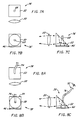
- a second embodiment of a reflective image plane module of the present invention is best illustrated in Figs. 3A-3C, designated generally by the reference character 52.
- the same or equivalent elements in this or succeeding embodiments will utilize the same numerals as previously described with respect to the reflective image plane module 30.
- the reflective image plane module 52 functions substantially the same as the reflective image plane module 30, as illustrated in Fig. 3C.
- the reflective image plane module 52 replaces the mirror 48 with a prism 56.
- the prism 56 includes a projection 58 formed in a first wall 60 thereof.
- the projection 58 includes a light receiving surface 62, through which the light is focused. As before, the light is acted upon and reflected by the wafer based active matrix 46 and again reflected by an inside surface 64 of the wall 60 to the lens 50.
- the projection 58 and the surface 62 form another optical element of the reflective image plane module 52.
- the surface 62 can be flat, can be a convex surface 62' or can be a concave surface 62'' as desired.
- the shape of the surface 62 is chosen to widen, narrow and/or direct the light beam.
- the reflective image plane module 52 is injection molded as an integral unit.
- the prism 56 and the wafer based active matrix 46 form the reflective image plane module 52.
- a third embodiment of a reflective image plane module of the present invention is best illustrated in Figs. 5A-5C and is designated generally by the reference numeral 66.
- the focused light beam utilizing the lens 34 and 36 would collect the most light, but the lens system encompasses a fairly large amount of space.
- the reflective image plane module 66 provides a very compact unit by eliminating the lens 34 and 36.
- a light source 68 such as a bulb, is mounted directly into the aperture 42 of the wall 40 of the reflective image plane module 66, which otherwise operates the same as the reflective image plane module 30. The light is reflected from the wafer based active matrix 46 to the mirror surface 48 to the lens 50.
- the light from the bulb 68 would be passed through the appropriate filter to provide the red, green or blue color component. Again, the light 68 and the lens 50 generally would not form part of the reflective image plane module 66.
- a further embodiment of a reflective image plane module of the present invention is best illustrated in Figs. 6A-6C and is designated generally by the reference numeral 70.
- the reflective image plane module 70 is somewhat of a compromise between the reflective image plane modules 30 and 66.
- a light source 72 is coupled into a fiber optic light guide or tube 74, which directs the light into the reflective image plane module 70 through the aperture 42, where it is acted upon like the reflective image plane module 30.
- the guide 74 gathers more light than utilizing the bulb 68, but encompasses more space than the bulb 68.
- the light guide 74 is more flexible and occupies less space than the lens system 34, 36.
- the bulb 68 can be utilized with the prism type reflective image plane module 52, as best illustrated in Figs. 7A-7C, forming another reflective image plane module embodiment of the present invention which is designated generally by the reference numeral 76.
- the operation of the reflective image plane module 76 is generally the same as the reflective image plane module 52, once the light is introduced to the reflective image plane module 76.
- the light guide 74 also can be utilized with the prism type reflective image plane module 52, as best illustrated in Figs. 8A-8C, forming a further reflective image plane module embodiment of the present invention which is designated generally by the reference numeral 78.
- the operation of the reflective image plane module 78 is generally the same as the reflective image plane module 52, once the light is introduced to the reflective image plane module 78.
- Each of the above reflective image plane modules can be utilized as part of a monochrome projection or imaging system or can form one reflective image plane module of a three lens color projection system embodiment of the present invention, for example, as illustrated in Fig. 9 and which is designated generally by the reference character 80.
- the projection system 80 and other projection systems are further described in EP-A-0486523.
- the projection system 80 includes a light source 82, such as a bulb and reflector, from which light is directed through a columnating lens or lens system 84 to form a beam of light 86.
- the light beam 86 includes all three light components red, blue and green (hereinafter R, B and G).
- the beam 86 is directed to a B dichroic mirror 88.
- the B light component 90 is reflected from the mirror 88 to a B reflective image plane module 92.
- the B reflective image plane module 92 can be any of the above-described reflective image plane modules 30, 52, 70 and 78.
- the encoded B light 94 is reflected from the B reflective image plane module 92 to a lens 96 and projected by the lens 96, to a screen 98, where it is combined with the other components to form a color image.
- a light beam 86' passes through the mirror 88 with the G & R light components therein.
- the light beam 86' is directed to a G dichroic mirror 100.
- the G light component 102 is reflected from the mirror 100 to a G reflective image plane module 104.
- the encoded G light 106 is reflected from the G reflective image plane module 104 to a lens 108 and projected by the lens 108 to the screen 98.
- a light beam 86'' passes through the mirror 100 with only the R component therein.
- the beam 86'' is directed to a mirror 110 and reflected therefrom to a R reflective image plane module 112.
- the encoded R light 114 is reflected from the R reflective image plane module 112 to a lens 116 and projected by the lens 116 to the screen 98.
- the information encoding is provided by an electronic interface 118 coupled to the reflective image plane modules 92, 104 an 112.
- FIG. 10 an embodiment of a single imaging, single lens projection system of the present invention is best illustrated and is designated generally by the reference numeral 120.
- a light source 122 of any of the above referenced types, provides light to a multicolor reflective image plane module 124.
- a fully encoded light beam 126 is output from the color reflective image plane module 124 and focused by a lens 128 onto the screen 98.
- the wafer based active matrix includes a mosaic or other type of color filter array integral therewith. This configuration would not currently be the most desirable, because three monochrome reflective image plane modules would triple the resolution on the screen 98 and would absorb much less heat than the single reflective image plane module 124.
- the projection system light source could be any suitable type of light source, such as xenon metal halide or quartz-halogen lights for example.
- the projection systems have been described, for example purposes, as front screen projection systems, but also could be rear screen configurations or utilize fiber optic expanders, where the light is projected onto an end of a fiber optic bundle.
- the reflective image plane modules can be formed separately or can be formed integrally connected together to form a full color module. It is therefore to be understood that within the scope of the appended claims, the invention may be practiced otherwise than as specifically described.
Landscapes
- Physics & Mathematics (AREA)
- General Physics & Mathematics (AREA)
- Engineering & Computer Science (AREA)
- Multimedia (AREA)
- Signal Processing (AREA)
- Liquid Crystal (AREA)
- Projection Apparatus (AREA)
- Devices For Indicating Variable Information By Combining Individual Elements (AREA)
Abstract
Claims (7)
- Module de plan d'image réfléchissant (30, 52, 66, 70, 76, 78) comprenant :un moyen réfléchissant de formation d'image (46) pour former un faisceau de lumière réfléchi d'une lumière traversant celui-ci et pour communiquer des informations audit faisceau de lumière réfléchi ;et un moyen (40, 42, 48 ; 58, 64) pour passer la lumière audit moyen réfléchissant de formation d'image et pour projeter ledit faisceau de lumière réfléchi pour une observation, caractérisé en ce que le moyen réfléchissant de formation d'image comprend une matrice active basée sur une plaquette et en ce que ladite plaquette (46) est un substrat de plaquette monocristallin de non transmission de lumière avec ladite matrice active formée sur une surface de ladite plaquette.
- Module selon la revendication 1, dans lequel ledit moyen de passage et de projection de lumière comprend un miroir (40) avec une ouverture (42) à l'intérieur de celui-ci pour diriger la lumière à travers ladite matrice active basée sur une plaquette (46), ledit miroir (40) formant au moins une partie dudit moyen de projection.
- Module de plan d'image réfléchissant (52, 76, 78) comprenant
un moyen réfléchissant de formation d'image (46), caractérisé en ce que le moyen réfléchissant de formation d'image comprend une matrice active basée sur une plaquette pour former un faisceau de lumière réfléchi à partir de la lumière traversant celui-ci et pour communiquer des informations audit faisceau de lumière réfléchi ; et en ce que le module comprend en outre un moyen (58, 64) pour passer la lumière sur ladite matrice active basée sur une plaquette et pour projeter ledit faisceau de lumière réfléchi pour une observation, ledit moyen de passage et de projection de lumière comprenant un prisme (56) avec une projection de réception de lumière (58) pour diriger la lumière, ledit prisme formant au moins une partie dudit moyen de projection. - Module selon la revendication 3, dans lequel ladite plaquette (46) est un substrat de plaquette monocristallin de non transmission de lumière avec ladite matrice active formée sur une surface de ladite plaquette.
- Module selon l'une quelconque des revendications 1, 2 ou 4, comprenant en outre un matériau LCD formé sur ladite matrice active, ledit matériau LCD formé à partir d'un matériau de modulation de lumière solide ayant des corps de matériau à cristaux liquides en suspension à l'intérieur de celui-ci.
- Module selon l'une quelconque des revendications précédentes, dans lequel ladite matrice active basée sur une plaquette (46) comprend un réseau de filtres couleurs pour former un faisceau de lumière de couleur réfléchi.
- Module selon la revendication 2 ou la revendication 3, caractérisé en outre par un système de lentilles (34) pour collimater de la lumière à partir d'une source lumineuse et pour focaliser la lumière à travers ladite projection (58) ou ladite ouverture (42).
Applications Claiming Priority (3)
| Application Number | Priority Date | Filing Date | Title |
|---|---|---|---|
| US392747 | 1989-08-11 | ||
| US07/392,747 US5024524A (en) | 1989-08-11 | 1989-08-11 | Reflective image plane module |
| PCT/US1990/004425 WO1991002998A1 (fr) | 1989-08-11 | 1990-08-07 | Module de plan d'image reflecteur |
Publications (3)
| Publication Number | Publication Date |
|---|---|
| EP0485435A1 EP0485435A1 (fr) | 1992-05-20 |
| EP0485435A4 EP0485435A4 (en) | 1992-06-24 |
| EP0485435B1 true EP0485435B1 (fr) | 1996-12-18 |
Family
ID=23551860
Family Applications (1)
| Application Number | Title | Priority Date | Filing Date |
|---|---|---|---|
| EP90911541A Revoked EP0485435B1 (fr) | 1989-08-11 | 1990-08-07 | Module pour un systeme reflechissant de modulation de lumiere |
Country Status (8)
| Country | Link |
|---|---|
| US (1) | US5024524A (fr) |
| EP (1) | EP0485435B1 (fr) |
| JP (1) | JPH04507009A (fr) |
| KR (1) | KR100196740B1 (fr) |
| AU (1) | AU6141190A (fr) |
| DE (1) | DE69029473T2 (fr) |
| FI (1) | FI920548A7 (fr) |
| WO (1) | WO1991002998A1 (fr) |
Families Citing this family (20)
| Publication number | Priority date | Publication date | Assignee | Title |
|---|---|---|---|---|
| DE69030872D1 (de) * | 1989-08-11 | 1997-07-10 | Raf Electronics Corp | Auf halbleiter basierte matritze |
| JP2828297B2 (ja) * | 1990-01-19 | 1998-11-25 | 旭光学工業株式会社 | 反射型プロジェクター |
| FR2669127B1 (fr) * | 1990-11-09 | 1993-01-22 | Thomson Csf | Projecteur d'images a deux faisceaux polarises par ecran matriciel. |
| US5426526A (en) * | 1991-04-05 | 1995-06-20 | Sharp Kabushiki Kaisha | Reflection type single crystal silicon substrate liquid crystal display device and system |
| US5307185A (en) * | 1992-05-19 | 1994-04-26 | Raychem Corporation | Liquid crystal projection display with complementary color dye added to longest wavelength imaging element |
| US5398081A (en) * | 1993-06-07 | 1995-03-14 | Raychem Corporation | Apparatus for projecting colored images |
| US5758941A (en) * | 1994-04-22 | 1998-06-02 | Stahl; Thomas D. | Pixel compensated electro-optical display system |
| US5557353A (en) * | 1994-04-22 | 1996-09-17 | Stahl; Thomas D. | Pixel compensated electro-optical display system |
| JPH08122750A (ja) * | 1994-10-19 | 1996-05-17 | Sharp Corp | 液晶電気光学装置、それを利用した投射型表示装置及びそれらの駆動方法 |
| US5818564A (en) * | 1996-09-13 | 1998-10-06 | Raychem Corporation | Assembly including an active matrix liquid crystal display module |
| US5971545A (en) * | 1997-06-25 | 1999-10-26 | Hewlett-Packard Company | Light source for projection display |
| US6046858A (en) * | 1997-10-16 | 2000-04-04 | Aurora Systems, Inc. | Light separation and recombination system for an off-axis projector |
| US6943203B2 (en) | 1998-03-02 | 2005-09-13 | Johnson & Johnson Vision Care, Inc. | Soft contact lenses |
| US6088380A (en) * | 1998-04-30 | 2000-07-11 | Spectra Science Corporation | Method and apparatus for intracavity pixelated lasing projection |
| US6246459B1 (en) | 1998-06-10 | 2001-06-12 | Tyco Electronics Corporation | Assembly including an active matrix liquid crystal display module and having plural environmental seals |
| KR100584538B1 (ko) * | 1999-11-04 | 2006-05-30 | 삼성전자주식회사 | 마이크로미러 가동장치를 채용한 반사형 프로젝터 |
| US6375330B1 (en) | 1999-12-30 | 2002-04-23 | Gain Micro-Optics, Inc. | Reflective liquid-crystal-on-silicon projection engine architecture |
| US20020176054A1 (en) * | 1999-12-30 | 2002-11-28 | Mihalakis George M. | Reflective liquid-crystal-on-silicon projection engine architecture |
| US7320521B2 (en) * | 2004-07-12 | 2008-01-22 | Next Wave Optics, Inc. | Optical engine architectures |
| US7530693B2 (en) * | 2005-05-31 | 2009-05-12 | Next Wave Optics Inc. | Single MEMS imager optical engine |
Family Cites Families (12)
| Publication number | Priority date | Publication date | Assignee | Title |
|---|---|---|---|---|
| US3525566A (en) * | 1968-07-24 | 1970-08-25 | Gerald Altman | Projection devices and graphic materials therefor |
| US3862360A (en) * | 1973-04-18 | 1975-01-21 | Hughes Aircraft Co | Liquid crystal display system with integrated signal storage circuitry |
| US4103297A (en) * | 1976-12-20 | 1978-07-25 | Hughes Aircraft Company | Light-insensitive matrix addressed liquid crystal display system |
| US4368963A (en) * | 1978-06-29 | 1983-01-18 | Michael Stolov | Multicolor image or picture projecting system using electronically controlled slides |
| US4239346A (en) * | 1979-05-23 | 1980-12-16 | Hughes Aircraft Company | Compact liquid crystal display system |
| GB2081018B (en) * | 1980-07-31 | 1985-06-26 | Suwa Seikosha Kk | Active matrix assembly for display device |
| JPS5961818A (ja) * | 1982-10-01 | 1984-04-09 | Seiko Epson Corp | 液晶表示装置 |
| JPS63101829A (ja) * | 1986-10-17 | 1988-05-06 | Nec Corp | アクテイブ・マトリツクス液晶表示装置およびその製造方法 |
| US4749259A (en) * | 1987-05-15 | 1988-06-07 | Hughes Aircraft Company | Liquid crystal image projection with multicolor prepolarizing system |
| DE3720375A1 (de) * | 1987-06-19 | 1988-12-29 | Fraunhofer Ges Forschung | Projektionsvorrichtung |
| US4826311A (en) * | 1987-07-24 | 1989-05-02 | Hughes Aircraft Company | Prism assembly with three periscopes and projection lenses for a single light valve full-color projector |
| NL8802517A (nl) * | 1988-10-13 | 1990-05-01 | Philips Nv | Beeldprojektie-inrichting. |
-
1989
- 1989-08-11 US US07/392,747 patent/US5024524A/en not_active Expired - Fee Related
-
1990
- 1990-08-07 DE DE69029473T patent/DE69029473T2/de not_active Revoked
- 1990-08-07 FI FI920548A patent/FI920548A7/fi not_active Application Discontinuation
- 1990-08-07 AU AU61411/90A patent/AU6141190A/en not_active Abandoned
- 1990-08-07 WO PCT/US1990/004425 patent/WO1991002998A1/fr not_active Ceased
- 1990-08-07 EP EP90911541A patent/EP0485435B1/fr not_active Revoked
- 1990-08-07 KR KR1019920700302A patent/KR100196740B1/ko not_active Expired - Fee Related
- 1990-08-07 JP JP2511152A patent/JPH04507009A/ja active Pending
Also Published As
| Publication number | Publication date |
|---|---|
| FI920548A0 (fi) | 1992-02-10 |
| WO1991002998A1 (fr) | 1991-03-07 |
| JPH04507009A (ja) | 1992-12-03 |
| FI920548A7 (fi) | 1992-02-10 |
| US5024524A (en) | 1991-06-18 |
| EP0485435A4 (en) | 1992-06-24 |
| AU6141190A (en) | 1991-04-03 |
| KR100196740B1 (ko) | 1999-06-15 |
| DE69029473D1 (de) | 1997-01-30 |
| DE69029473T2 (de) | 1997-05-15 |
| EP0485435A1 (fr) | 1992-05-20 |
Similar Documents
| Publication | Publication Date | Title |
|---|---|---|
| US5022750A (en) | Active matrix reflective projection system | |
| US5108172A (en) | Active matrix reflective image plane module and projection system | |
| US5024524A (en) | Reflective image plane module | |
| US5353133A (en) | A display having a standard or reversed schieren microprojector at each picture element | |
| JP4386989B2 (ja) | 液晶表示装置 | |
| KR100281249B1 (ko) | 액티브매트릭스기판, 이 기판을 사용한 액정장치 및 이 액정장치를 사용하는 표시장치 | |
| US5806950A (en) | Compact high resolution light valve projector | |
| JPH10254370A (ja) | 表示パネル及びそれを用いた投射型表示装置 | |
| JPH0435048B2 (fr) | ||
| US5430562A (en) | Liquid crystal light valve including between light and light valve microlenses and two reflecting layers with a matrix of openings | |
| EP0438565B1 (fr) | Matrice active basee sur une tranche | |
| JPS61150487A (ja) | 液晶ビデオ・プロジエクタ | |
| US5781252A (en) | Dual light valve color projector system | |
| US6575576B1 (en) | Method and apparatus for increasing the spatial resolution of a projected pixelated display | |
| JPH0727132B2 (ja) | プロジエクタ | |
| KR940000591B1 (ko) | 투사형 칼라 영상표시장치 | |
| JPH083583B2 (ja) | 投写型カラ−表示装置 | |
| JPH0519347A (ja) | 投写型画像表示装置 | |
| JPH09265106A (ja) | 液晶ディスプレイパネルおよび投射型液晶表示装置 | |
| JP2746267B2 (ja) | 投写型カラー表示装置の製造方法 | |
| JP2001133747A (ja) | 液晶装置とこれを用いた液晶表示装置 | |
| JP2827653B2 (ja) | 投影型液晶表示装置 | |
| JPH11126035A (ja) | 表示装置、液晶表示装置及びそれを用いた液晶プロジェクター | |
| JPH01209481A (ja) | 画像投影用液晶パネル構造 | |
| JPH03198037A (ja) | 高精細投影型表示装置 |
Legal Events
| Date | Code | Title | Description |
|---|---|---|---|
| PUAI | Public reference made under article 153(3) epc to a published international application that has entered the european phase |
Free format text: ORIGINAL CODE: 0009012 |
|
| 17P | Request for examination filed |
Effective date: 19920305 |
|
| AK | Designated contracting states |
Kind code of ref document: A1 Designated state(s): DE FR GB NL |
|
| A4 | Supplementary search report drawn up and despatched |
Effective date: 19920508 |
|
| AK | Designated contracting states |
Kind code of ref document: A4 Designated state(s): DE FR GB NL |
|
| 17Q | First examination report despatched |
Effective date: 19940720 |
|
| GRAG | Despatch of communication of intention to grant |
Free format text: ORIGINAL CODE: EPIDOS AGRA |
|
| GRAH | Despatch of communication of intention to grant a patent |
Free format text: ORIGINAL CODE: EPIDOS IGRA |
|
| GRAH | Despatch of communication of intention to grant a patent |
Free format text: ORIGINAL CODE: EPIDOS IGRA |
|
| GRAA | (expected) grant |
Free format text: ORIGINAL CODE: 0009210 |
|
| AK | Designated contracting states |
Kind code of ref document: B1 Designated state(s): DE FR GB NL |
|
| PG25 | Lapsed in a contracting state [announced via postgrant information from national office to epo] |
Ref country code: NL Free format text: LAPSE BECAUSE OF FAILURE TO SUBMIT A TRANSLATION OF THE DESCRIPTION OR TO PAY THE FEE WITHIN THE PRESCRIBED TIME-LIMIT Effective date: 19961218 |
|
| REF | Corresponds to: |
Ref document number: 69029473 Country of ref document: DE Date of ref document: 19970130 |
|
| ET | Fr: translation filed | ||
| NLV1 | Nl: lapsed or annulled due to failure to fulfill the requirements of art. 29p and 29m of the patents act | ||
| PLBQ | Unpublished change to opponent data |
Free format text: ORIGINAL CODE: EPIDOS OPPO |
|
| PLBI | Opposition filed |
Free format text: ORIGINAL CODE: 0009260 |
|
| PLBF | Reply of patent proprietor to notice(s) of opposition |
Free format text: ORIGINAL CODE: EPIDOS OBSO |
|
| 26 | Opposition filed |
Opponent name: PHILIPS ELECTRONICS N.V. Effective date: 19970917 |
|
| PLBF | Reply of patent proprietor to notice(s) of opposition |
Free format text: ORIGINAL CODE: EPIDOS OBSO |
|
| PLBF | Reply of patent proprietor to notice(s) of opposition |
Free format text: ORIGINAL CODE: EPIDOS OBSO |
|
| PLBF | Reply of patent proprietor to notice(s) of opposition |
Free format text: ORIGINAL CODE: EPIDOS OBSO |
|
| PGFP | Annual fee paid to national office [announced via postgrant information from national office to epo] |
Ref country code: FR Payment date: 19990719 Year of fee payment: 10 |
|
| PGFP | Annual fee paid to national office [announced via postgrant information from national office to epo] |
Ref country code: GB Payment date: 19990721 Year of fee payment: 10 Ref country code: DE Payment date: 19990721 Year of fee payment: 10 |
|
| RDAH | Patent revoked |
Free format text: ORIGINAL CODE: EPIDOS REVO |
|
| RDAG | Patent revoked |
Free format text: ORIGINAL CODE: 0009271 |
|
| STAA | Information on the status of an ep patent application or granted ep patent |
Free format text: STATUS: PATENT REVOKED |
|
| 27W | Patent revoked |
Effective date: 20000226 |
|
| GBPR | Gb: patent revoked under art. 102 of the ep convention designating the uk as contracting state |
Free format text: 20000226 |
|
| PLAB | Opposition data, opponent's data or that of the opponent's representative modified |
Free format text: ORIGINAL CODE: 0009299OPPO |