EP0485617B1 - Hysterese schaltung - Google Patents
Hysterese schaltung Download PDFInfo
- Publication number
- EP0485617B1 EP0485617B1 EP91909705A EP91909705A EP0485617B1 EP 0485617 B1 EP0485617 B1 EP 0485617B1 EP 91909705 A EP91909705 A EP 91909705A EP 91909705 A EP91909705 A EP 91909705A EP 0485617 B1 EP0485617 B1 EP 0485617B1
- Authority
- EP
- European Patent Office
- Prior art keywords
- transistor
- switching circuit
- resistor
- circuit
- terminal
- Prior art date
- Legal status (The legal status is an assumption and is not a legal conclusion. Google has not performed a legal analysis and makes no representation as to the accuracy of the status listed.)
- Expired - Lifetime
Links
- 238000010586 diagram Methods 0.000 description 3
- 230000003247 decreasing effect Effects 0.000 description 1
- 230000000694 effects Effects 0.000 description 1
- 230000007257 malfunction Effects 0.000 description 1
Images


Classifications
-
- H—ELECTRICITY
- H03—ELECTRONIC CIRCUITRY
- H03K—PULSE TECHNIQUE
- H03K17/00—Electronic switching or gating, i.e. not by contact-making and –breaking
-
- H—ELECTRICITY
- H03—ELECTRONIC CIRCUITRY
- H03K—PULSE TECHNIQUE
- H03K17/00—Electronic switching or gating, i.e. not by contact-making and –breaking
- H03K17/51—Electronic switching or gating, i.e. not by contact-making and –breaking characterised by the components used
- H03K17/56—Electronic switching or gating, i.e. not by contact-making and –breaking characterised by the components used by the use, as active elements, of semiconductor devices
- H03K17/72—Electronic switching or gating, i.e. not by contact-making and –breaking characterised by the components used by the use, as active elements, of semiconductor devices having more than two PN junctions; having more than three electrodes; having more than one electrode connected to the same conductivity region
- H03K17/73—Electronic switching or gating, i.e. not by contact-making and –breaking characterised by the components used by the use, as active elements, of semiconductor devices having more than two PN junctions; having more than three electrodes; having more than one electrode connected to the same conductivity region for DC voltages or currents
- H03K17/732—Measures for enabling turn-off
-
- H—ELECTRICITY
- H03—ELECTRONIC CIRCUITRY
- H03K—PULSE TECHNIQUE
- H03K17/00—Electronic switching or gating, i.e. not by contact-making and –breaking
- H03K17/30—Modifications for providing a predetermined threshold before switching
- H03K17/305—Modifications for providing a predetermined threshold before switching in thyristor switches
Definitions
- This invention relates to a hysteresis circuit comprising a positive feedback circuit having first and second input terminals and an output terminal;
- the Schmitt Trigger, circuit is well known as a switching circuit which operates in a hysteretic manner.
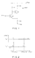
- Fig. 1 shows an example of the Schmitt Trigger circuit.
- the base of an npn transistor Q1 is connected to an input terminal Vin.
- a resistor R1 has one end connected to the collector of the transistor Q1, and the other end connected to a power source terminal V DD .
- a resistor R2 has one end connected to the emitter of the transistor Q1 and the other end connected to an earth terminal Vss.
- the base of an npn transistor Q2 is connected to the collector of the transistor Q1, while the collector of the transistor Q2 is connected to an output terminal Vout.
- a resistor R3 has one end connected to the collector of the transistor Q2 and the other end connected to the power source terminal V DD .
- the emitter of the transistor Q2 is connected to the one end of the resistor R2.
- the maximum hysteresis error of the above circuit is determined by the values of the resistors R1 - R3.
- the output voltage of the circuit varies from a low voltage (hereinafter called “L”) to a high voltage (hereinafter called “H”) when the transistor Q1 is turned on, while it varies from “H” to "L” when the transistor Q2 is turned on. That is, when one of the transistors Q1 t and Q2 is on, the other is off.
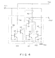
- the Schmitt Trigger circuit shown in Fig. 1 operates in a hysteretic manner as shown in Fig. 2. Then, this operation will be explained with reference to Figs. 1 and 2.
- the output voltage Vout varies in the order of a, b, c, d, and e in Fig. 2.
- the output voltage Vout varies in the order of e, d, f, b, and a in Fig. 2.
- the values of the resistors R1 and R3 are determined so as to satisfy the following formula (3): Vth(L ⁇ H) > Vth(H ⁇ L.) R1 > R3
- the threshold voltage V th(L ⁇ H) assumed when the output voltage varies from “L” to “H” is determined by the resistance ratio between the resistors R1 and R3.
- the threshold voltage V th(H ⁇ L) assumed when the output voltage varies from “H” to “L” is determined by the resistance ratio between the resistors R1 and R2. Accordingly, the threshold voltages V th(L ⁇ H) and V th(H ⁇ L) depend upon each other, and hence must be set to values falling within a very narrow range.
- the Schmitt Trigger circuit comprises an integrated circuit
- great variations may exist among Schmitt Trigger circuits if the ratio of the largest resistance of the resistors R1 - R3 to the smallest resistance of them is set to a large value.
- the threshold voltages V th(L ⁇ H) and V th(H ⁇ L) vary in accordance with a change in the power source voltage V DD .
- a constant voltage source dedicated for supplying the threshold voltages is required in the integrated circuit.
- the hysteresis circuit initially defined is characterised in that the positive feedback circuit is a thyristor circuit operable to output a low voltage from the output terminal when in an on-state and to output a high voltage from the output terminal when in a off-state, wherein the thyristor circuit comprises a first transistor having an emitter connected to the output terminal, a collector connected to the second input terminal and a base connected to the first input terminal, a second transistor having a collector connected to the base of the first transistor, an emitter connected to an earth terminal, and a base connected to the second input terminal, a first resistor connected between the base and emitter of the first transistor, a second resistor having one end connected to a power source terminal and the other end connected to the output terminal, and a third resistor connected between the base and emitter of the second transistor, the respective threshold voltages being defined independently of the voltage on said power source terminal by a respective pair of resistors constituting an input voltage divider in the first and second switching circuits, respectively.
- the threshold voltages of the first and second switch circuits can be set independently of each other, and do not vary in accordance with a change in the voltage source, so that the conditions of hysteresis can be determined in a simple manner.
- Fig. 1 is a circuit diagram, showing a conventional hysteresis circuit
- Fig. 2 is a view, showing a hysteresis characteristic of the hysteresis circuit of Fig. 1
- Fig. 3 is a circuit diagram, showing a hysteresis circuit according to an embodiment of the invention
- Fig. 4 is a circuit diagram, showing a switching circuit in detail
- Fig. 5 is a view, showing a hysteresis characteristic of the hysteresis circuit of Fig. 3.
- Fig. 3 shows a hysteresis circuit according to the embodiment.
- a pnp transistor Q1 has an emitter connected to an output terminal Vout.
- An npn transistor Q2 has a collector connected to the base of the transistor Q1, and an emitter connected to an earth terminal Vss.
- a resistor R1 has one end connected to the base of the transistor Q1, and the other end connected to the emitter of the same.
- a resistor R2 has one end connected to a power source terminal V DD , and the other end connected to the output terminal Vout.
- a resistor R3 has one end connected to the base of the transistor Q2, and the other end connected to the emitter of the same.
- the transistors Q1 and Q2, and the resistors R1 - R3 form a thyristor circuit 101.
- the resistors R1 and R3 are provided for preventing malfunction of the circuit due to leak current, while the resistor R2 is the load resistor of the circuit.
- the thyristor circuit 101 is a positive feedback circuit, so that it cannot shift to an on-stage independently.
- a switching circuit 102 is provided to turn on the thyristor circuit.
- the input of the switching circuit 102 is connected to the input terminal Vin, and the output of the same is connected to the base of the transistor Q1 of the thyristor circuit 101.
- a switching circuit 103 is provided for turning off the thyristor circuit 101.
- the input of the switching circuit 103 is connected to the input terminal Vin, while the output of the same is connected to the base of the transistor Q2 of the thyristor circuit 101.
- the threshold voltages of the switching circuits 102 and 103 can be determined independently of each other. If these threshold voltages are set to different values, hysteretic operation can be performed.
- Fig. 4 shows in detail the switching circuits 102 and 103 incorporated in the hysteresis circuit shown in Fig. 3.
- the switching circuit 102 comprises an npn transistor Q3 and resistors R4 and R5.
- the transistor Q3 has a collector connected to the base of the transistor Q1, and an emitter connected to the earth terminal Vss.
- the resistor R4 has an end connected to the base of the transistor Q3, and the other end connected to the earth terminal Vss.
- the resistor R5 has an end connected to the base of the transistor Q3, and the other end connected to the input terminal Vin.
- the transistor Q3 is provided for turning on the thyristor 101, i.e., for shifting the output voltage from "H" to "L”.
- the resistors R4 and R5 are provided for determining the threshold voltage of the switching circuit 102.
- the switching circuit 103 comprises transistors Q4 and Q5 and resistors R6 - R8.
- the transistor Q4 is an npn type, and has a collector connected to the base of the transistor Q2, and an emitter connected to the earth terminal Vss.
- the resistor R6 has an end connected to the base of the transistor Q4, and the other end connected to the power source terminal V DD .
- the transistor Q5 is an npn type, and has a collector connected to the base of the transistor Q4, and an emitter connected to the earth terminal Vss.
- the transistor Q5 serves as an inverter.
- the resistor R7 has an end connected to the base of the transistor Q5, and the other end connected to the earth terminal Vss.
- the resistor R8 has an end connected to the base of the transistor Q5, and the other end connected to the input terminal Vin.
- the transistor Q5 inverts the logical values of the switching circuits 102 and 103.
- the transistors Q4 and Q5 turn off the thyristor circuit 101, i.e., shift the output voltage from "L” to "H”.
- the resistor R6 is a bias resistor for the transistor Q4, while the resistors R7 and R8 determine the threshold voltage of the switching circuit 103.
- the threshold voltages of the switching circuits 102 and 103 can be determined independently of each other in accordance with a change in the input signal. Accordingly, the hysteresis width can be set easily and freely.
- the hysteresis circuit shown in Fig. 4 performs a hysteretic operation as shown in Fig. 5. This operation will be explained with reference to Figs. 4 and 5.
- V BEQ3 ⁇ Vin ⁇ R4/(R4 + R5) where reference code V BEQ3 represents the threshold voltage of the transistor Q3.
- the output voltage Vout varies in the order of a, b, c, d, and e in Fig. 5.
- the thyristor circuit 101 When the thyristor circuit 101 is once turned on, it is kept on by virtue of its positive feedback function, irrespective of the on/off state of the transistor Q3 (i.e., even though the input voltage Vin is lower than V th(H ⁇ L) ).
- V BEQ5 Vin ⁇ R7/(R7 + R8) where reference code V BEQ5 represents the threshold voltage of the transistor Q5.
- the output voltage Vout varies in the order of e, d, f, b and a in Fig. 5.
- the thyristor circuit 101 When the thyristor circuit 101 is once turned off, it is kept off by virtue of its positive feedback function, irrespective of the on/off state of the transistor Q4 (i.e., even though the input voltage Vin exceeds V th(L ⁇ H) ).
- the threshold voltage V th(L ⁇ H) assumed when the output voltage varies from “L” to “H” and the threshold voltage Vth(H ⁇ L) assumed when the output voltage varies from “H” to “L” will be determined independently of each other, as is evident from the formulas (4) and (5).
- the resistance ratio of the resistor R4 to the resistor R5 and that of the resistor R7 to the resistor R8 can be determined at a high degree of freedom, to determine the threshold voltages.
- threshold voltages V th(H ⁇ L) and V th(L ⁇ H) vary independently from a change in the power source voltage V DD , no constant voltage sources are required. It is needless to say that the threshold voltages V th(H ⁇ L) and V th(L ⁇ H) may be set to vary in accordance with the power source voltage V DD .
Landscapes
- Manipulation Of Pulses (AREA)
- Electronic Switches (AREA)
- Measurement Of Current Or Voltage (AREA)
Claims (5)
- Eine Hystereseschaltung umfassend:einen positiven Rückkopplungskreis (101) mit ersten und zweiten Anschlüssen und einem Ausgangsanschluß (Vout);einen ersten Schaltkreis (102), dessen Ausgang mit dem ersten Eingangsanschluß verbunden ist, wobei der Schaltkreis den Rückkopplungskreis nur dann einschaltet, wenn eine Eingangsspannung an einem Eingang des ersten Schaltkreises über eine Schwellwertspannung des ersten Schaltkreises hinausgeht; undeinen zweiten Schaltkreis (103), dessen Ausgang mit dem zweiten Eingangsanschluß verbunden ist, wobei der zweite Schaltkreis den Rückkopplungskreis nur dann ausschaltet, wenn die Eingangsspannung an einem Eingang des zweiten Schaltkreises niedriger ist als ein Schwellwert des zweiten Schaltkreises, worin die Schwellwertspannung des Schaltkreises unterschiedlich ist von der des zweiten Schaltkreises, worin die Eingänge des ersten und zweiten Schaltkreises miteinander und mit einem Eingangsanschluß (Vin) der Hystereseschaltung verbunden sind, und worin die jeweiligen Schwellwertspannungen unabhängig voneinander eingestellt werden können,dadurch gekennzeichnet, daß
der positive Rückkopplungskreis eine Thyristorschaltung ist, die dergestalt betreibbar ist, daß sie eine niedrige Spannung von dem Ausgangsanschluß ausgibt wenn sie in einem EIN Zustand ist, und eine hohe Spannung von dem Ausgangsanschluß ausgibt wenn sie in einem AUS Zustand ist, worin die Thyristorschaltung einen ersten Transistor (Q1) umfaßt, der einen Emitter aufweist, der mit dem Ausgangsanschluß verbunden ist, einen Kollektor, der mit dem zweiten Eingangsanschluß verbunden ist, und eine Basis, die mit dem ersten Eingangsanschluß verbunden ist, einen zweiten Transistor (Q2), der einen Kollektor aufweist, der mit der Basis des ersten Transistors verbunden ist, einen Emitter, der mit einem Erdungsanschluß (Vss) verbunden ist, und eine Basis, die mit dem zweiten Eingangsanschluß verbunden ist, einen ersten Widerstand (R1), der über die Basis und den Emitter des ersten Transistors geschaltet ist, und einen zweiten Widerstand (R2), dessen eines Ende mit einem Stromquellenanschluß verbunden ist und dessen anderes Ende mit dem Ausgangsanschluß verbunden ist, und einen dritten Widerstand (R3), der über die Basis und den Emitter des zweiten Transistors geschaltet ist, wobei die entsprechenden Schwellwertspannungen unabhängig von der Spannung des Stromquellenanschlusses jeweils mittels eines jeweiligen Paars von Widerständen (R4, R5; R7, R8), die einen Eingangsspannungsteiler bilden, in dem ersten oder zweiten Schaltkreis bestimmt werden. - Eine Hystereseschaltung gemäß Anspruch 1,
dadurch gekennzeichnet , daß
der erste Schaltkreis einen Transistor (Q3) umfaßt mit einem Kollektor, der mit dem ersten Eingangsanschluß verbunden ist und einem Emitter, der mit einem Erdungsanschluß verbunden ist, einen ersten Widerstand (R4), dessen eines Ende mit der Basis des Transistors verbunden ist und dessen anderes Ende mit dem Erdungsanschluß verbunden ist, und einen zweiten Widerstand (R5), dessen eines Ende mit der Basis des Transistors verbunden ist und dessen anderes Ende mit einem Eingangsanschluß verbunden ist, um ein Eingangssignal zu empfangen, und worin der zweite Schaltkreis einen ersten Transistor (Q4) umfaßt mit einem Kollektor, der mit dem zweiten Eingangsanschluß verbunden ist, und einem Emitter, der mit einem Erdungsanschluß verbunden ist, einen ersten Widerstand (R6), dessen eines Ende mit der Basis von dem ersten Transistor verbunden ist und dessen anderes Ende mit dem Stromquellenanschluß verbunden ist, einen zweiten Transistor (Q5) mit einem Kollektor, der mit der Basis des ersten Transistors verbunden ist und einem Emitter, der mit dem Erdungsungsanschluß verbunden ist, einen zweiten Widerstand (R7), dessen eines Ende mit der Basis von dem zweiten Transistor verbunden ist und dessen anderes Ende mit dem Erdungsanschluß verbunden ist, und einen dritten Widerstand (R8), dessen eines Ende mit der Basis von dem zweiten Widerstand verbunden ist und dessen anderes Ende mit einem Eingangsanschluß verbunden ist, um ein Eingangssignal zu empfangen. - Eine Hystereseschaltung gemäß Anspruch 2,
dadurch gekennzeichnet , daß der Schwellwert des ersten Schaltkreises (102) mittels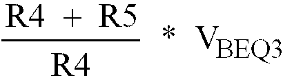
- Eine Hystereseschaltung gemäß Anspruch 2 oder 3,
dadurch gekennzeichnet , daß der Schwellwert des zweiten Schaltkreises (103) mittels
- Eine Hystereseschaltung gemäß Anspruch 2, 3 oder 4,
dadurch gekennzeichnet , daß der Schwellwert des Transistors (Q3) von dem ersten Schaltkreis (102) gleich dem Schwellwert des zweiten Transistors (Q5) von dem zweiten Schaltkreis (103) ist, worin der erste Widerstand (R4) und ein zweiter Widerstand (R5) des ersten Schaltkreises (102) und der zweite Widerstand (R7) und der dritte Widerstand (R8) des zweiten Schaltelements (103) die folgende Beziehung erfüllen:
Applications Claiming Priority (3)
| Application Number | Priority Date | Filing Date | Title |
|---|---|---|---|
| JP136704/90 | 1990-05-25 | ||
| JP2136704A JP2573394B2 (ja) | 1990-05-25 | 1990-05-25 | ヒステリシス回路 |
| PCT/JP1991/000693 WO1991019354A1 (fr) | 1990-05-25 | 1991-05-23 | Circuit d'hysteresis |
Publications (3)
| Publication Number | Publication Date |
|---|---|
| EP0485617A1 EP0485617A1 (de) | 1992-05-20 |
| EP0485617A4 EP0485617A4 (en) | 1993-05-05 |
| EP0485617B1 true EP0485617B1 (de) | 1997-12-17 |
Family
ID=15181533
Family Applications (1)
| Application Number | Title | Priority Date | Filing Date |
|---|---|---|---|
| EP91909705A Expired - Lifetime EP0485617B1 (de) | 1990-05-25 | 1991-05-23 | Hysterese schaltung |
Country Status (6)
| Country | Link |
|---|---|
| US (1) | US5287014A (de) |
| EP (1) | EP0485617B1 (de) |
| JP (1) | JP2573394B2 (de) |
| KR (1) | KR940002861B1 (de) |
| DE (1) | DE69128456T2 (de) |
| WO (1) | WO1991019354A1 (de) |
Families Citing this family (6)
| Publication number | Priority date | Publication date | Assignee | Title |
|---|---|---|---|---|
| US5204541A (en) * | 1991-06-28 | 1993-04-20 | Texas Instruments Incorporated | Gated thyristor and process for its simultaneous fabrication with high- and low-voltage semiconductor devices |
| US6020767A (en) * | 1998-05-04 | 2000-02-01 | International Business Machines Corporation | CMOS chip to chip settable interface receiver cell |
| US6462971B1 (en) * | 1999-09-24 | 2002-10-08 | Power Integrations, Inc. | Method and apparatus providing a multi-function terminal for a power supply controller |
| JP2002287832A (ja) * | 2001-03-27 | 2002-10-04 | Sharp Corp | 送信装置 |
| CN103944542A (zh) * | 2013-01-22 | 2014-07-23 | 浙江海得新能源有限公司 | 一种晶闸管辅助关断装置 |
| US11575379B2 (en) * | 2021-03-23 | 2023-02-07 | Delphi Technologies Ip Limited | Switch with hysteresis |
Family Cites Families (13)
| Publication number | Priority date | Publication date | Assignee | Title |
|---|---|---|---|---|
| US3310686A (en) * | 1963-06-14 | 1967-03-21 | Rca Corp | Flip flip circuits utilizing set-reset dominate techniques |
| US3392290A (en) * | 1965-07-21 | 1968-07-09 | Ibm | Bistable device employing transistors of complementary types |
| JPS4410690Y1 (de) * | 1966-10-31 | 1969-04-30 | ||
| US3816767A (en) * | 1973-03-23 | 1974-06-11 | Electrospace Corp | Schmitt trigger circuit |
| JPS5346587B2 (de) * | 1974-02-14 | 1978-12-14 | ||
| JPS5186954A (ja) * | 1975-01-29 | 1976-07-30 | Takeda Riken Ind Co Ltd | Shingoreberukenshutsusochi |
| JPS5389350A (en) * | 1977-01-17 | 1978-08-05 | Mitsubishi Electric Corp | Schmitt trigger circuit |
| US4115707A (en) * | 1977-03-31 | 1978-09-19 | Rca Corporation | Circuit for single-line control of GTO controlled rectifier conduction |
| JPS553210A (en) * | 1978-06-21 | 1980-01-11 | Toshiba Corp | Waveform shaping circuit |
| US4572968A (en) * | 1983-03-04 | 1986-02-25 | Motorola, Inc. | SCR Fire sensitivity control and fire control apparatus |
| JPS60114024A (ja) * | 1983-11-26 | 1985-06-20 | Sanyo Electric Co Ltd | ヒステリシス回路 |
| JPS60208119A (ja) * | 1984-03-30 | 1985-10-19 | Hitachi Ltd | 容量性負荷の駆動回路 |
| JPS6331216A (ja) * | 1986-07-25 | 1988-02-09 | Hitachi Ltd | パルス発生回路 |
-
1990
- 1990-05-25 JP JP2136704A patent/JP2573394B2/ja not_active Expired - Lifetime
-
1991
- 1991-05-23 US US07/809,526 patent/US5287014A/en not_active Expired - Lifetime
- 1991-05-23 DE DE69128456T patent/DE69128456T2/de not_active Expired - Lifetime
- 1991-05-23 WO PCT/JP1991/000693 patent/WO1991019354A1/ja not_active Ceased
- 1991-05-23 EP EP91909705A patent/EP0485617B1/de not_active Expired - Lifetime
- 1991-05-24 KR KR1019910008415A patent/KR940002861B1/ko not_active Expired - Fee Related
Non-Patent Citations (1)
| Title |
|---|
| Halbleiter-Schaltungstechnik, Tietze & Schenk, p.162-164, Springer Verlag, 1983 * |
Also Published As
| Publication number | Publication date |
|---|---|
| DE69128456T2 (de) | 1998-05-07 |
| DE69128456D1 (de) | 1998-01-29 |
| US5287014A (en) | 1994-02-15 |
| WO1991019354A1 (fr) | 1991-12-12 |
| EP0485617A1 (de) | 1992-05-20 |
| EP0485617A4 (en) | 1993-05-05 |
| JP2573394B2 (ja) | 1997-01-22 |
| KR940002861B1 (ko) | 1994-04-04 |
| JPH0435216A (ja) | 1992-02-06 |
| KR910021022A (ko) | 1991-12-20 |
Similar Documents
| Publication | Publication Date | Title |
|---|---|---|
| US4977381A (en) | Differential relaxation oscillator | |
| US3848139A (en) | High-gain comparator circuit | |
| EP0497319A1 (de) | Integrierte Halbleiter-Schaltungseinheit mit Detektionsschaltung für Substrat-Potential | |
| US3988595A (en) | High-gain differential input comparator with emitter feedback input hysteresis | |
| GB2199677A (en) | Bandgap voltage reference circuit | |
| EP0084722B1 (de) | Differenzverstärkerschaltungsanordnung | |
| EP0155720B1 (de) | Kaskadenstromquellenanordnung | |
| US4268789A (en) | Limiter circuit | |
| EP0485617B1 (de) | Hysterese schaltung | |
| US4339674A (en) | Trigger circuit | |
| JPS5938773B2 (ja) | レベルシフト回路 | |
| US4645999A (en) | Current mirror transient speed up circuit | |
| EP0379092B1 (de) | Spannungsgeneratorschaltung | |
| EP0528659B1 (de) | Impedanzvervielfacher | |
| US5099139A (en) | Voltage-current converting circuit having an output switching function | |
| EP0343553B1 (de) | Niederspannungsgesteuerte elektronische Schaltung in Bereitschaftsstellung mit verzögertem Abschalten | |
| US5075567A (en) | Electronic switch circuit | |
| US4453140A (en) | Oscillator using charge-discharge characteristics of a transistor junction | |
| US5666076A (en) | Negative input voltage comparator | |
| JPH029373Y2 (de) | ||
| SU940303A1 (ru) | Транзисторный ключ | |
| SU508933A1 (ru) | Устройство дл управлени ключом | |
| KR950008531Y1 (ko) | 아날로그 신호의 선택 스위칭회로 | |
| KR900002357Y1 (ko) | Am 검파회로 | |
| KR200167174Y1 (ko) | 동작모드 절환회로 |
Legal Events
| Date | Code | Title | Description |
|---|---|---|---|
| PUAI | Public reference made under article 153(3) epc to a published international application that has entered the european phase |
Free format text: ORIGINAL CODE: 0009012 |
|
| 17P | Request for examination filed |
Effective date: 19920124 |
|
| AK | Designated contracting states |
Kind code of ref document: A1 Designated state(s): DE FR GB |
|
| A4 | Supplementary search report drawn up and despatched |
Effective date: 19930317 |
|
| AK | Designated contracting states |
Kind code of ref document: A4 Designated state(s): DE FR GB |
|
| RAP1 | Party data changed (applicant data changed or rights of an application transferred) |
Owner name: TOSHIBA AVE CO., LTD Owner name: KABUSHIKI KAISHA TOSHIBA |
|
| 17Q | First examination report despatched |
Effective date: 19960223 |
|
| GRAG | Despatch of communication of intention to grant |
Free format text: ORIGINAL CODE: EPIDOS AGRA |
|
| GRAG | Despatch of communication of intention to grant |
Free format text: ORIGINAL CODE: EPIDOS AGRA |
|
| GRAH | Despatch of communication of intention to grant a patent |
Free format text: ORIGINAL CODE: EPIDOS IGRA |
|
| GRAH | Despatch of communication of intention to grant a patent |
Free format text: ORIGINAL CODE: EPIDOS IGRA |
|
| GRAA | (expected) grant |
Free format text: ORIGINAL CODE: 0009210 |
|
| AK | Designated contracting states |
Kind code of ref document: B1 Designated state(s): DE FR GB |
|
| REF | Corresponds to: |
Ref document number: 69128456 Country of ref document: DE Date of ref document: 19980129 |
|
| ET | Fr: translation filed | ||
| PLBE | No opposition filed within time limit |
Free format text: ORIGINAL CODE: 0009261 |
|
| STAA | Information on the status of an ep patent application or granted ep patent |
Free format text: STATUS: NO OPPOSITION FILED WITHIN TIME LIMIT |
|
| 26N | No opposition filed | ||
| REG | Reference to a national code |
Ref country code: GB Ref legal event code: IF02 |
|
| PGFP | Annual fee paid to national office [announced via postgrant information from national office to epo] |
Ref country code: GB Payment date: 20100329 Year of fee payment: 20 |
|
| PGFP | Annual fee paid to national office [announced via postgrant information from national office to epo] |
Ref country code: FR Payment date: 20100525 Year of fee payment: 20 |
|
| PGFP | Annual fee paid to national office [announced via postgrant information from national office to epo] |
Ref country code: DE Payment date: 20100519 Year of fee payment: 20 |
|
| REG | Reference to a national code |
Ref country code: DE Ref legal event code: R071 Ref document number: 69128456 Country of ref document: DE |
|
| REG | Reference to a national code |
Ref country code: GB Ref legal event code: PE20 Expiry date: 20110522 |
|
| PG25 | Lapsed in a contracting state [announced via postgrant information from national office to epo] |
Ref country code: GB Free format text: LAPSE BECAUSE OF EXPIRATION OF PROTECTION Effective date: 20110522 |
|
| PG25 | Lapsed in a contracting state [announced via postgrant information from national office to epo] |
Ref country code: DE Free format text: LAPSE BECAUSE OF EXPIRATION OF PROTECTION Effective date: 20110524 |