EP0485969B1 - Schaltkreise zur Strombegrenzung - Google Patents
Schaltkreise zur Strombegrenzung Download PDFInfo
- Publication number
- EP0485969B1 EP0485969B1 EP91119327A EP91119327A EP0485969B1 EP 0485969 B1 EP0485969 B1 EP 0485969B1 EP 91119327 A EP91119327 A EP 91119327A EP 91119327 A EP91119327 A EP 91119327A EP 0485969 B1 EP0485969 B1 EP 0485969B1
- Authority
- EP
- European Patent Office
- Prior art keywords
- transistor
- emitter
- current
- power device
- whose
- Prior art date
- Legal status (The legal status is an assumption and is not a legal conclusion. Google has not performed a legal analysis and makes no representation as to the accuracy of the status listed.)
- Expired - Lifetime
Links
- 239000008186 active pharmaceutical agent Substances 0.000 description 9
- 238000010586 diagram Methods 0.000 description 6
- 101100422538 Escherichia coli sat-2 gene Proteins 0.000 description 4
- 108091006503 SLC26A1 Proteins 0.000 description 4
- 230000004048 modification Effects 0.000 description 4
- 238000012986 modification Methods 0.000 description 4
- 238000004519 manufacturing process Methods 0.000 description 3
- XAGFODPZIPBFFR-UHFFFAOYSA-N aluminium Chemical compound [Al] XAGFODPZIPBFFR-UHFFFAOYSA-N 0.000 description 2
- 229910052782 aluminium Inorganic materials 0.000 description 2
- 230000007423 decrease Effects 0.000 description 2
- 230000003321 amplification Effects 0.000 description 1
- 230000001419 dependent effect Effects 0.000 description 1
- 238000009792 diffusion process Methods 0.000 description 1
- 238000000034 method Methods 0.000 description 1
- 238000003199 nucleic acid amplification method Methods 0.000 description 1
- 229910021420 polycrystalline silicon Inorganic materials 0.000 description 1
- 229920005591 polysilicon Polymers 0.000 description 1
Images



Classifications
-
- G—PHYSICS
- G01—MEASURING; TESTING
- G01R—MEASURING ELECTRIC VARIABLES; MEASURING MAGNETIC VARIABLES
- G01R19/00—Arrangements for measuring currents or voltages or for indicating presence or sign thereof
- G01R19/165—Indicating that current or voltage is either above or below a predetermined value or within or outside a predetermined range of values
- G01R19/16566—Circuits and arrangements for comparing voltage or current with one or several thresholds and for indicating the result not covered by subgroups G01R19/16504, G01R19/16528, G01R19/16533
- G01R19/16576—Circuits and arrangements for comparing voltage or current with one or several thresholds and for indicating the result not covered by subgroups G01R19/16504, G01R19/16528, G01R19/16533 comparing DC or AC voltage with one threshold
Definitions
- the present invention relates to current-limiting circuits for limiting the output current of a power device when the low voltages rises above a predetermined value.
- US 3,930,172 discloses an input supply independent circuit having a first transistor, whose base and connector are connected to each other, a second transistor, whose collector is connected to the emitter of said first transistor, a third transistor, whose base is connected to the base of said first transistor and whose emitter is connected to the base of said first transistor and a fourth transistor, whose base is connected to the emitter of said first transistor and whose collector is connected to the emitter of said third transistor.
- the circuit operates as a voltage regulator, wherein the voltage developed across a resistor in the emitter path of one of the transistors has a value other than zero, if the emitter areas of the transistors are of different values.
- Fig. 1 shows a power device T 1 designed to function as a main switch, and also a current-limiting circuit 11 for limiting the current flowing through the power device T 1 .
- the current-limiting circuit 11 comprises a lateral NPN transistor Q 1 and two resistors R 1 and R 2 (e.g., diffusion resistors, polysilicon registers, or aluminum wiring).
- this circuit 11 can be formed on a chip, by a method substantially identical to the method of manufacturing a discrete power transistor.
- the current-limiting circuit 11 can restrict the output current I O of the power device T 1 . More precisely, when the output current I O increases over the value I OL given below, the transistor Q 1 is turned on, thereby limiting the output current I O of the power device T 1 .
- Fig. 2 shows a power device T 1 designed to function as a main switch and developed to solve the problem with the circuit shown in Fig. 1, and also a current-limiting circuit 11 identical to the circuit 11 shown in Fig. 1, used for limiting the current flowing through the power device T 1 .
- the power device T 1 comprises a plurality of small cells. The small cells are divided into two groups, the first consisting of n times as many cells as the the second group, where n is a number greater than 1. Hence, the output current I O of the device T 1 is divided into two two parts having magnitudes n and 1, respectively. Hence, the current I O ', defined below, is supplied to the resistor R 2 .
- I O ' 1 N + 1 ⁇ I O
- the object of the invention is to provide a current-limiting circuit for limiting the output current of an intermediate or high power transistor with low total power loss.
- a current-limiting circuit comprising, besides a power device having a control electrode : a first resistor connected at one end to the control electrode of the power device, and at the other end to the voltage source for the low-voltage detecting circuit; a second resistor connected to the output of the power device, for detecting the output current of the power device; and a third resistor connected at one end to the voltage source, and at the other end to the collector of the first transistor of the low-voltage detecting circuit.
- the collector of the third transistor is connected to the control electrode of the power device.
- the emitter of the second transistor is connected to the first end of the second resistor.
- the emitter of the fourth transistor is connected to the second end of the second resistor.
- a current-limiting circuit comprising: a power device having a control electrode for receiving a control input; a resistor for detecting an output current of said power device, said resistor having a first end connected to the power device and a second end; a first transistor whose base and collector are connected to each other, and whose collector is connected to a current source; a second transistor whose collector is connected to the emitter of said first transistor, and whose emitter is connected to the first end of said resistor; a third transistor whose base is connected to the base of said first transistor, and whose emitter is connected to the base of said second transistor; and a fourth transistor whose base is connected to the emitter of said first transistor, whose collector is connected to the emitter of said third transistor and whose emitter is connected to the second end of said resistor, wherein an output signal is output from the collector of said third transistor when the output current of said power device increases over a predetermined value to limit the output current of said power device in response thereto.
- a current-limiting circuit comprising:
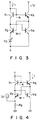
- Fig. 3 shows an example of a low-voltage detecting circuit, which comprises four lateral NPN transistors Q 1 , Q 2 , Q 3 , and Q 4 .
- the transistor Q 3 has an emitter area N times greater than that of the transistor Q 1 , where N is a number other than 1.
- the transistor Q 2 has an emitter area M times greater than that of the transistor Q 4 .
- a current I 1 is supplied to the transistors Q 1 and Q 2 , operating these transistors, and also to the base of the transistor Q 3 .
- the low-voltage detecting circuit is designed to detect a low voltage V 0 .
- a control current I 2 flows through the circuit when the low voltage V 0 rises above a predetermined value V OL .
- the voltage V OL can be calculated as follows, from the base-emitter voltages of the transistors Q 1 to Q 4 .
- V OL kT q ln(N ⁇ M)
- Equation (12) shows that the voltage V OL does not depend on the current I 2 . Rather, it is determined by the ratio of the emitter area of the transistor Q 1 to that of the transistor Q 3 , and also by the ratio of the emitter area of the transistor Q 2 to that of the transistor Q 4 .
- the power loss of the low-voltage detecting circuit can be less than that of the conventional one, since the voltage V OL can be far lower than the base-emitter voltage of, for example, the transistor Q 1 shown in Fig. 1.
- the control current i2 and the detected voltage V 0 can have the following relationships:
- Fig. 4 shows a modification of the low-voltage detecting circuit shown in Fig. 3.
- This circuit is identical to the circuit of Fig. 3, except that a resistor R 2 and a current source I 0 are used in place of the low voltage V 0 .
- the control current I2 can flow through the transistors Q 3 and Q 4 .
- I OL 1 R2 ⁇ kT q ln(M ⁇ N)
- Fig. 5 shows a circuit which is designed to limit the output current of a power transistor and having the low-voltage detecting circuit shown in Fig. 1 according to an embodiment of the invention.
- the output current I 0 of a power MOSFET T 1 is supplied to a resistor R 2 , thereby detecting the low voltage applied to a resistor R 2 .
- V OL I OL ⁇ R 2 , where I OL is the maximum current the power MOSFET T 1 can output.
- the current I 2 flowing through the transistors Q 3 and Q 4 are substantially nil.
- the gate-source voltage V GS of the power MOSFET T 1 is V 1 - R 2 ⁇ I 0 , where V 1 is the voltage applied to a terminal 12, which is higher than the voltage V GS(ON) required to turn on the power MOSFET T 1 . Since R 2 ⁇ I 0 has an extremely small value, V GS is nearly equal to V 1 . Thus, the power MOSFET T 1 is on at all times, and its output current I O is not limited at all.
- the output current I O is equal to or greater than the maximum output current I OL (namely, I O ⁇ I OL )
- the current I 2 flowing through the transistors Q 3 and Q 4 increases greatly.
- the gate voltage V G of the power MOSFET T 1 changes to V 1 - R 1 ⁇ I 2 .
- the gate-source voltage V GS of the power MOSFET T 1 changes to about V 1 - R 1 ⁇ I 2 .
- the power MOSFET T 1 is turned off when the voltage V GS falls below the voltage V GS(ON) . Then, the output current I O of the power MOSFET T 1 is limited.
- Fig. 6 represents the relationship between the gate-source voltage V GS and output current I 0 of the power MOSFET T 1 .
- the gate-source voltage VGS abruptly falls when the output current I 0 increases over the maximum value I OL .
- the output current I 0 of the power MOSFET T 1 is limited.
- the power MOSFET and the current-limiting circuit for limiting the output current of the MOSFET can be fabricated in one and the same step of the method of manufacturing an ordinary discrete power transistor.
- the resistor R 2 can be formed of an aluminum wire or a bonding wire.
- the power device is not limited to a power MOSFET, and can be a bipolar type transistor e.g., insulated gate bipolar transistor.
- the circuit shown in Fig. 7 is characterized in that the small cells constituting a power transistor T1 are divided into two groups. The first consisting of n times as many cells as the second group, where n is a number greater than 1.
- the output current I O of the power device T 1 is, therefore, divided into two parts having magnitudes n and 1, respectively.
- the current I O ' defined below, is supplied to the resistor R 2 .
- 1/(n+1) of the current I O flows to a resistor R 2 , thereby generating a low voltage V O .
- this current-limiting circuit even if the output current I O is too large, it is unnecessary to decrease the resistance of the resistor R 2 in order to obtain the low voltage V O . This helps to reduce the difference in resistance among the resistors which are to be used as resistor R 2 .
- the circuit shown in Fig. 8 is characterized in that a control output is obtained from the collector of a transistor Q 3 .
- This current-limiting circuit serves effectively, not only to limit the output current I O of the power MOSFET T 1 , but also to utilize the output current I O with high efficiency.
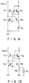
- Figs. 9 and 10 show two further examples of low-voltage detecting circuits.
- a low voltage V O is applied to the emitter of the transistor Q 2
- the ground voltage is applied to the emitter of the transistor Q 4 .
- This circuit is, there fore, a "low positive-voltage detecting circuit.”
- the ground voltage is applied to the emitter of a transistor Q 2
- a low voltage V O is applied to the emitter of a transistor Q 4 .
- the circuit is, there fore, a "low negative-voltage detecting circuit.”
- V O > V OL where V O is the detected voltage and V OL is a predetermined voltage
- I DET 0 if V O ⁇ V OL , I DET > 0.
- the circuit can, therefore, detect the low voltage V O .
- the low-voltage detecting circuit shown in Fig. 10 is, so to speak, a modification of the circuit shown in Fig. 9.
- the low voltage V O generated by a resistor R 2 and a current source I O .
- a control current I DET can flow through transistors Q 1 and Q 2 , as can be understood from equation (15).
- the control current I DET cannot flow through the transistor Q 1 or Q 2 , as can be understood from equation (16).
- the above low-voltage detecting circuit can detect the low voltage V OL which is determined by the ratio of the emitter area of the transistor Q 1 to that of the transistor Q 3 , and also by the ratio of the emitter area of the transistor Q 2 to that of the transistor Q 4 .
- the circuit serves to limit the output current of a power device.
- the power MOSFET and the current-limiting circuit both incorporated in the embodiments of Figs. 5 and 7, can be fabricated in one and the same step of the method of manufacturing an ordinary discrete power transistor.
- the embodiments of Figs. 5 and 7 can, therefore, provide a power device having a current-limiting section.
Landscapes
- Engineering & Computer Science (AREA)
- Power Engineering (AREA)
- Physics & Mathematics (AREA)
- General Physics & Mathematics (AREA)
- Measurement Of Current Or Voltage (AREA)
- Electronic Switches (AREA)
- Manipulation Of Pulses (AREA)
- Continuous-Control Power Sources That Use Transistors (AREA)
- Emergency Protection Circuit Devices (AREA)
- Amplifiers (AREA)
Claims (7)
- Strombegrenzungsschaltung, umfassend:eine Leistungseinrichtung (T1) mit einer Steuerelektrode;einen ersten Widerstand (R1), der an einem Ende mit der Steuerelektrode der Leistungseinrichtung (T1) und an dem anderen Ende mit einer Potentialquelle (V1) verbunden ist;einen zweiten Widerstand (R2) zum Erfassen eines Stromausgangs (I0) von der Leistungseinrichtung (T1);einen ersten Transistor (Q1), dessen Basis und Kollektor zusammengeschaltet sind;einen zweiten Transistor (Q2), dessen Kollektor mit dem Emitter des ersten Transistors (Q1) verbunden ist und dessen Emitter mit einem Ende des zweiten Widerstands (R2) verbunden ist;einen dritten Transistor (Q3), dessen Basis mit der Basis des ersten Transistors (Q1) verbunden ist und dessen Kollektor mit der Steuerelektrode der Leistungseinrichtung (T1) verbunden ist und dessen Emitter mit der Basis des zweiten Transistors (Q2) verbunden ist;einen vierten Transistor (Q4), dessen Basis mit dem Emitter des ersten Transistors (Q1) verbunden ist und dessen Kollektor mit dem Emitter des dritten Transistors (Q3) verbunden ist und dessen Emitter mit dem anderen Ende des zweiten Transistors (Q2) verbunden ist; undeinen dritten Widerstand (R3), der an einem Ende mit der Potentialquelle (V1) und an dem anderen Ende mit dem Kollektor des ersten Transistors (Q1) verbunden ist,wobei der Ausgangsstrom (I0) der Leistungseinrichtung (T1) begrenzt wird, wenn der Ausgangsstrom (I0) der Leistungseinrichtung (T1) über einen vorgegebenen Wert ansteigt.
- Schaltung nach Anspruch 1, dadurch gekennzeichnet, daß das Verhältnis der Emitterfläche des ersten Transistors (Q1) zu derjenigen des dritten Transistors (Q3) 1:N ist, wobei N eine Zahl größer als 1 ist und wobei das Verhältnis der Emitterfläche des zweiten Transistors (Q2) zu derjenigen des vierten Transistors (Q4) M:1 ist, wobei M eine andere Zahl als 1 ist.
- Schaltung nach Anspruch 1, dadurch gekennzeichnet, daß die Leistungseinrichtung (T1) ein Leistungs-MOSFET ist.
- Schaltung nach Anspruch 1, dadurch gekennzeichnet, daß der Ausgangsstrom (I0) in zwei Teile aufgeteilt ist, wobei der erste Teil n-mal so groß wie der zweite Teil ist, wobei n eine Zahl größer als 1 ist und wobei ein Strom von I0/(n+1) an den zweiten Widerstand (R2) fließt.
- Schaltung, umfassend:eine Leistungseinrichtung (T1) mit einer Steuerelektrode zum Empfangen eines Steuereingangs;einen Widerstand (R2) zum Erfassen eines Ausgangsstroms (I0) der Leistungseinrichtung (T1), wobei der Widerstand (R2) ein mit der Leistungseinrichtung (T1) verbundenes erstes Ende und ein zweites Ende aufweist;einen ersten Transistor (Q1), dessen Basis und Kollektor zusammengeschaltet sind und dessen Kollektor mit einer Stromquelle (I) verbunden ist;einen zweiten Transistor (Q2), dessen Kollektor mit den Emitter des ersten Transistors (Q1) verbunden ist und dessen Emitter mit dem ersten Ende des Widerstands (Q2) verbunden ist;einen dritten Transistor (Q3), dessen Basis mit der Basis des ersten Transistors (Q1) verbunden ist und dessen Emitter mit der Basis des zweiten Transistors (Q2) verbunden ist;einen vierten Transistor (Q4), dessen Basis mit dem Emitter des ersten Transistors (Q1) verbunden ist, dessen Kollektor mit dem Emitter des dritten Transistors (Q3) verbunden ist und dessen Emitter mit dem zweiten Ende des Widerstands (R2) verbunden ist,wobei ein Ausgangssignal (AUSGANG) von dem Kollektor des dritten Transistors (Q3) ausgegeben wird, wenn der Ausgangsstrom (I0) der Leistungseinrichtung (T1) über einen vorgegebenen Wert ansteigt, um den Ausgangsstrom der Leistungseinrichtung im Ansprechen darauf zu begrenzen.
- Schaltung nach Anspruch 5, wobei das Verhältnis der Emitterfläche des ersten Transistors (Q1) zu derjenigen des dritten Transistors (Q3) 1:N ist, wobei N eine andere Zahl als 1 ist und wobei das Verhältnis der Emitterfläche des zweiten Transistors (Q2) zu derjenigen des vierten Transistors (Q4) M:1 ist, wobei M eine andere Zahl als 1 ist.
- Schaltung nach Anspruch 5, dadurch gekennzeichnet, daß die Leistungseinrichtung (T1) ein Leistungs-MOSFET ist.
Applications Claiming Priority (4)
| Application Number | Priority Date | Filing Date | Title |
|---|---|---|---|
| JP31087590 | 1990-11-16 | ||
| JP310875/90 | 1990-11-16 | ||
| JP3272199A JP2755848B2 (ja) | 1990-11-16 | 1991-10-21 | 微小電圧検出回路およびこれを用いた電流制限回路 |
| JP272199/91 | 1991-10-21 |
Publications (3)
| Publication Number | Publication Date |
|---|---|
| EP0485969A2 EP0485969A2 (de) | 1992-05-20 |
| EP0485969A3 EP0485969A3 (en) | 1992-10-28 |
| EP0485969B1 true EP0485969B1 (de) | 1997-07-23 |
Family
ID=26550080
Family Applications (1)
| Application Number | Title | Priority Date | Filing Date |
|---|---|---|---|
| EP91119327A Expired - Lifetime EP0485969B1 (de) | 1990-11-16 | 1991-11-13 | Schaltkreise zur Strombegrenzung |
Country Status (4)
| Country | Link |
|---|---|
| US (1) | US5402020A (de) |
| EP (1) | EP0485969B1 (de) |
| JP (1) | JP2755848B2 (de) |
| DE (1) | DE69126948T2 (de) |
Families Citing this family (4)
| Publication number | Priority date | Publication date | Assignee | Title |
|---|---|---|---|---|
| US5828261A (en) * | 1996-11-13 | 1998-10-27 | Caterpillar Inc. | Gate drive circuit that controls a power transistor in three states |
| JP2006086211A (ja) * | 2004-09-14 | 2006-03-30 | Denso Corp | 半導体装置 |
| US8598920B2 (en) * | 2009-05-19 | 2013-12-03 | Mitsubishi Electric Corporation | Gate driving circuit |
| US20230396150A1 (en) * | 2020-10-22 | 2023-12-07 | Lumineq Oy | Nfet half bridge circuit, and arrangement and use related to nfet half bridge circuit |
Citations (1)
| Publication number | Priority date | Publication date | Assignee | Title |
|---|---|---|---|---|
| US3930172A (en) * | 1974-11-06 | 1975-12-30 | Nat Semiconductor Corp | Input supply independent circuit |
Family Cites Families (7)
| Publication number | Priority date | Publication date | Assignee | Title |
|---|---|---|---|---|
| US3845405A (en) * | 1973-05-24 | 1974-10-29 | Rca Corp | Composite transistor device with over current protection |
| JPS584489B2 (ja) * | 1978-12-30 | 1983-01-26 | 富士通株式会社 | スイッチング回路 |
| US4590392A (en) * | 1983-09-19 | 1986-05-20 | Honeywell Inc. | Current feedback Schottky logic |
| US4533845A (en) * | 1984-02-22 | 1985-08-06 | Motorola, Inc. | Current limit technique for multiple-emitter vertical power transistor |
| DE3433538A1 (de) * | 1984-09-13 | 1986-03-20 | Telefunken electronic GmbH, 7100 Heilbronn | Schutzschaltung fuer einen vom laststrom durchflossenen leistungstransistor |
| FR2619972B1 (fr) * | 1987-08-31 | 1992-01-03 | Boudionny Anatoli | Etage amplificateur differentiel et configurations de circuits utilisant un tel etage |
| US5111071A (en) * | 1989-10-19 | 1992-05-05 | Texas Instruments Incorporated | Threshold detection circuit |
-
1991
- 1991-10-21 JP JP3272199A patent/JP2755848B2/ja not_active Expired - Fee Related
- 1991-11-13 EP EP91119327A patent/EP0485969B1/de not_active Expired - Lifetime
- 1991-11-13 DE DE69126948T patent/DE69126948T2/de not_active Expired - Lifetime
-
1994
- 1994-05-13 US US08/242,056 patent/US5402020A/en not_active Expired - Lifetime
Patent Citations (1)
| Publication number | Priority date | Publication date | Assignee | Title |
|---|---|---|---|---|
| US3930172A (en) * | 1974-11-06 | 1975-12-30 | Nat Semiconductor Corp | Input supply independent circuit |
Also Published As
| Publication number | Publication date |
|---|---|
| JP2755848B2 (ja) | 1998-05-25 |
| DE69126948T2 (de) | 1997-12-11 |
| US5402020A (en) | 1995-03-28 |
| EP0485969A2 (de) | 1992-05-20 |
| JPH053424A (ja) | 1993-01-08 |
| DE69126948D1 (de) | 1997-08-28 |
| EP0485969A3 (en) | 1992-10-28 |
Similar Documents
| Publication | Publication Date | Title |
|---|---|---|
| EP0419093B1 (de) | Strommessschaltung | |
| US4429339A (en) | AC Transistor switch with overcurrent protection | |
| US4977333A (en) | Power semiconductor device including an arrangement for controlling load current by independent control of a plurality of semiconductor elements | |
| EP0155720B1 (de) | Kaskadenstromquellenanordnung | |
| US4420786A (en) | Polarity guard circuit | |
| WO1993017492A1 (fr) | Circuit de detection de courant permettant de detecter la valeur d'un courant s'ecoulant du circuit de sortie d'un circuit integre | |
| KR100190353B1 (ko) | Mos 형 전력 트랜지스터에서의 전류 검출회로 | |
| USRE37778E1 (en) | Current limiting circuit | |
| EP0091307A2 (de) | Konstanter Strom- oder Spannungsquellentransistorkreis | |
| JPH03259614A (ja) | 電力デバイスの動作温度における事前調整依存性を有するmos型電力デバイスの短絡に対する保護装置 | |
| EP0485969A2 (de) | Unterspannungsdetektor | |
| US6054845A (en) | Current limiting circuit | |
| EP0618658B1 (de) | Thermischer Schutzschaltung | |
| US6480038B1 (en) | Bipolar comparator | |
| US4758820A (en) | Semiconductor circuit | |
| JP3309039B2 (ja) | インバータ制御装置の過電流保護回路 | |
| KR950010410B1 (ko) | 미소전압 검지회로 | |
| JPH0718892B2 (ja) | 電子スイツチの過電流検出回路 | |
| JPS5924195Y2 (ja) | トランジスタ回路 | |
| JPS643079Y2 (de) | ||
| JPH0611107B2 (ja) | スイッチング回路 | |
| JPS6110315A (ja) | 半導体集積回路装置 | |
| JPH06113441A (ja) | 電流検出回路 | |
| JPH05290591A (ja) | ツェナーメモリ装置 | |
| JPH09313672A (ja) | 磁性物体検出回路 |
Legal Events
| Date | Code | Title | Description |
|---|---|---|---|
| PUAI | Public reference made under article 153(3) epc to a published international application that has entered the european phase |
Free format text: ORIGINAL CODE: 0009012 |
|
| 17P | Request for examination filed |
Effective date: 19911113 |
|
| AK | Designated contracting states |
Kind code of ref document: A2 Designated state(s): DE FR GB |
|
| PUAL | Search report despatched |
Free format text: ORIGINAL CODE: 0009013 |
|
| AK | Designated contracting states |
Kind code of ref document: A3 Designated state(s): DE FR GB |
|
| 17Q | First examination report despatched |
Effective date: 19960508 |
|
| GRAG | Despatch of communication of intention to grant |
Free format text: ORIGINAL CODE: EPIDOS AGRA |
|
| GRAH | Despatch of communication of intention to grant a patent |
Free format text: ORIGINAL CODE: EPIDOS IGRA |
|
| GRAH | Despatch of communication of intention to grant a patent |
Free format text: ORIGINAL CODE: EPIDOS IGRA |
|
| GRAA | (expected) grant |
Free format text: ORIGINAL CODE: 0009210 |
|
| AK | Designated contracting states |
Kind code of ref document: B1 Designated state(s): DE FR GB |
|
| REF | Corresponds to: |
Ref document number: 69126948 Country of ref document: DE Date of ref document: 19970828 |
|
| ET | Fr: translation filed | ||
| PLBE | No opposition filed within time limit |
Free format text: ORIGINAL CODE: 0009261 |
|
| STAA | Information on the status of an ep patent application or granted ep patent |
Free format text: STATUS: NO OPPOSITION FILED WITHIN TIME LIMIT |
|
| 26N | No opposition filed | ||
| REG | Reference to a national code |
Ref country code: GB Ref legal event code: 746 Effective date: 19980917 |
|
| REG | Reference to a national code |
Ref country code: FR Ref legal event code: D6 |
|
| REG | Reference to a national code |
Ref country code: GB Ref legal event code: IF02 |
|
| PGFP | Annual fee paid to national office [announced via postgrant information from national office to epo] |
Ref country code: FR Payment date: 20101123 Year of fee payment: 20 |
|
| PGFP | Annual fee paid to national office [announced via postgrant information from national office to epo] |
Ref country code: DE Payment date: 20101110 Year of fee payment: 20 |
|
| PGFP | Annual fee paid to national office [announced via postgrant information from national office to epo] |
Ref country code: GB Payment date: 20101110 Year of fee payment: 20 |
|
| REG | Reference to a national code |
Ref country code: DE Ref legal event code: R071 Ref document number: 69126948 Country of ref document: DE |
|
| REG | Reference to a national code |
Ref country code: DE Ref legal event code: R071 Ref document number: 69126948 Country of ref document: DE |
|
| REG | Reference to a national code |
Ref country code: GB Ref legal event code: PE20 Expiry date: 20111112 |
|
| PG25 | Lapsed in a contracting state [announced via postgrant information from national office to epo] |
Ref country code: GB Free format text: LAPSE BECAUSE OF EXPIRATION OF PROTECTION Effective date: 20111112 |
|
| PG25 | Lapsed in a contracting state [announced via postgrant information from national office to epo] |
Ref country code: DE Free format text: LAPSE BECAUSE OF EXPIRATION OF PROTECTION Effective date: 20111114 |