EP0485973B1 - Konstantstromquellen-Schaltkreis - Google Patents
Konstantstromquellen-Schaltkreis Download PDFInfo
- Publication number
- EP0485973B1 EP0485973B1 EP91119333A EP91119333A EP0485973B1 EP 0485973 B1 EP0485973 B1 EP 0485973B1 EP 91119333 A EP91119333 A EP 91119333A EP 91119333 A EP91119333 A EP 91119333A EP 0485973 B1 EP0485973 B1 EP 0485973B1
- Authority
- EP
- European Patent Office
- Prior art keywords
- transistor
- current
- current path
- mos transistor
- gate
- Prior art date
- Legal status (The legal status is an assumption and is not a legal conclusion. Google has not performed a legal analysis and makes no representation as to the accuracy of the status listed.)
- Expired - Lifetime
Links
- 238000006243 chemical reaction Methods 0.000 claims description 7
- 230000000295 complement effect Effects 0.000 claims 1
- 238000010586 diagram Methods 0.000 description 8
- 230000000694 effects Effects 0.000 description 4
- 230000008878 coupling Effects 0.000 description 3
- 238000010168 coupling process Methods 0.000 description 3
- 238000005859 coupling reaction Methods 0.000 description 3
- 230000003247 decreasing effect Effects 0.000 description 2
- 230000004048 modification Effects 0.000 description 2
- 238000012986 modification Methods 0.000 description 2
Images


Classifications
-
- H—ELECTRICITY
- H03—ELECTRONIC CIRCUITRY
- H03K—PULSE TECHNIQUE
- H03K17/00—Electronic switching or gating, i.e. not by contact-making and –breaking
- H03K17/04—Modifications for accelerating switching
-
- H—ELECTRICITY
- H03—ELECTRONIC CIRCUITRY
- H03K—PULSE TECHNIQUE
- H03K17/00—Electronic switching or gating, i.e. not by contact-making and –breaking
- H03K17/04—Modifications for accelerating switching
- H03K17/041—Modifications for accelerating switching without feedback from the output circuit to the control circuit
- H03K17/04106—Modifications for accelerating switching without feedback from the output circuit to the control circuit in field-effect transistor switches
-
- H—ELECTRICITY
- H03—ELECTRONIC CIRCUITRY
- H03K—PULSE TECHNIQUE
- H03K17/00—Electronic switching or gating, i.e. not by contact-making and –breaking
- H03K17/51—Electronic switching or gating, i.e. not by contact-making and –breaking characterised by the components used
- H03K17/56—Electronic switching or gating, i.e. not by contact-making and –breaking characterised by the components used by the use, as active elements, of semiconductor devices
- H03K17/687—Electronic switching or gating, i.e. not by contact-making and –breaking characterised by the components used by the use, as active elements, of semiconductor devices the devices being field-effect transistors
- H03K17/693—Switching arrangements with several input- or output-terminals, e.g. multiplexers, distributors
Definitions
- the present invention relates to a switching constant current source circuit, used especially in a unit current source for, e.g., a digital-to-analog converter, for outputting an arbitrarily set current value in accordance with, e.g., an externally input selection code.
- a switching constant current source circuit used especially in a unit current source for, e.g., a digital-to-analog converter, for outputting an arbitrarily set current value in accordance with, e.g., an externally input selection code.
- a switching constant current source circuit used in a DAC is basically a circuit for always electrically connecting a current set at a predetermined value to one of a current output terminal and a dummy current output terminal by switching so as not to largely vary a current source.
- Fig. 1 shows an arrangement of a conventional switching constant current source circuit, which is disclosed in U.S. Patent No. 4,831,282.
- the source of a p-channel MOS transistor 71 is connected to a power source voltage VDD.
- the gate of the transistor 71 is applied with a reference voltage Vref71.
- the drain of the transistor 71 is connected to the sources of p-channel MOS transistors 72 and 73.
- the gate of the transistor 72 is applied with a digital code Cod corresponding to "1" or "0" as a logical amplitude.
- the drain of the transistor 72 serves as a dummy current output terminal Idmy connected to a ground voltage GND.
- the gate of the transistor 73 is applied with a reference voltage Vref73.
- the drain of the transistor 73 is connected to a current output terminal Iout.
- a digital code signal Cod for enabling the transistor 72 is applied to the gate of the transistor 72. If the ON resistance of the transistor 72 is smaller than the ON resistance of the transistor 73, most of the current is output to the terminal Idmy through the transistor 72. Therefore, in the output mode to the dummy current output terminal Idmy, the potential at a node 74 need only be lower than that at the node 74 in an output mode to the current output terminal Iout. Therefore, if the potential at that time is designed to be equal to or lower than the reference voltage Vref71, the transistor 73 is disabled, and current leakage can be prevented.
- a digital code signal Cod for disabling the transistor 72 is applied to the gate of the transistor 72.
- the influence of the mirror effect by a coupling capacitance MC serves to increase the ON/OFF operation speed in the transistor 72 upon switching based on the amplitude of the digital code signal Cod.
- the difference between the gate-source voltage and the drain-source voltage of the transistor 73 is increased in synchronism with the gradually increased potential at the node 74, and a stable current is output to the current output terminal Iout (reference numeral 83 in Fig. 2).
- the output current output from the current output terminal Iout at that time is determined by the ON resistances (low impedance) of the transistors 71 and 73 controlled by the predetermined reference voltages Vref71 and Vref73.
- a digital code signal Cod for enabling the transistor 72 is applied to the gate of the transistor 72.
- the switching operation of the transistor 72 is accelerated due to the influence of the mirror effect in the same manner as described above (reference numeral 84 in Fig. 2).
- the ON resistance of the transistor 72 becomes smaller than the ON resistance of the transistor 73, and most of the current flows to the dummy current output terminal Idmy. As a result, the potential at the node 74 is decreased, and the transistor 73 is disabled (reference numeral 86 in Fig. 2).
- the ON/OFF operation of the transistor 73 depends on a speed defined by the potential drift at the node 74 caused by the ON/OFF operation of the transistor 72. More specifically, the gate-drain voltage and the drain-source voltage of the transistor 73 are passively changed due to the potential drift at the node 74. For this reason, slow current changes indicated by reference numerals 82, 83, 85, and 86 in Fig. 2 disturb a high-speed operation.
- EP-A-0 356 570 shows a current mirror circuit including two MOS transistors with their respective gates connected. A third MOS transistor is series connected in the output path. An operational amplifier receives the drain potentials of the first two transistors and drives the gate of the third.
- the present invention has been made in consideration of the above situation, and'has as its object to provide a switching constant current source circuit capable of performing a high-speed switching operation.
- the present invention applies a variable gate bias to the second MOS transistor by utilizing the fact that the first MOS transistor, which is enabled/disabled in response to a digital signal, gives a change in voltage in the first current path.
- the ON/OFF operation of the second MOS transistor is positively controlled.
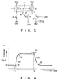
- Fig. 3 is a circuit diagram showing an arrangement of a switching constant current source.
- the sources of p-channel MOS transistors 11 and 12 are connected to a power source voltage VDD.
- the gates of the transistors 11 and 12 are commonly connected to each other.
- the gate and the drain of the transistor 11 are connected to each other.
- the drain of the transistor 11 is connected to a ground voltage GND through a constant current source 13. More specifically, the transistors 11 and 12 constitute a current mirror circuit for the constant current source 13.
- the drain of the transistor 12 is connected to the sources of p-channel MOS transistors 14 and 15.
- the gate of the transistor 15 is applied with a digital code signal Cod corresponding to "1" or "0" as a logical amplitude.
- the drain of the transistor 15 is connected to the ground voltage GND, and serves as a dummy current output terminal Idmy.
- the gate of the transistor 14 is connected to the output terminal of an amplifier 16.
- the non-inverting input terminal of the amplifier 16 is connected to the common gate of the transistors 11 and 12, and the inverting input terminal thereof is connected to the drain of the transistor 12.
- the drain of the transistor 14 is connected to a current output terminal Iout.
- the transistor 15 When a current is output to the dummy current output terminal Idmy, the transistor 15 receives a code input for cutting off the transistor 15 at time t1. At this time, the potential at a node 18 is instantaneously; rapidly increased due to the mirror effect of the coupling capacitance of the transistor 15.
- the amplifier 16 senses the slight potential rise at the node 18 after a short operation delay period 21, and the output from the amplifier 16 changes to about 0 V at which the transistor 14 is enabled. Thus, a current is rapidly increased, as indicated by reference numeral 22 in Fig. 4. Thereafter, the amplifier 16 operates, so that the potential at a node 17 gradually becomes equal to the potential at the node 18.
- the output is initially increased at an inclination indicated by reference numeral 22, and the increase in output is rapidly reduced so as to suppress a glitch, as indicated by reference numeral 23.
- the amplifier 16 applies a bias (imaginary short bias) for equalizing the voltages at the nodes 17 and 18 to the transistor 14. Therefore, in this state, the drain voltage of the transistor 12 is controlled, so that the operation state of the transistor 11 as a reference current source and the operation state of the transistor 12 as a current mirror become equal to each other.
- the transistor 15 receives a code input for enabling the transistor 15 at time t2
- the potential at the node 17 is rapidly decreased due to the mirror effect of the coupling capacitance.
- the output from the current output terminal lout rapidly changes, as indicated by reference numeral 25, and the change in output is then decelerated and stabilized, as indicated by reference numeral 26.
- Fig. 5 is another circuit diagram of a switching constant current source.
- the present invention is applied to a current pull-in type circuit.
- n-channel MOS transistors 31, 32, 34, and 35 are used.
- an amplifier 36 and a constant current source 33 are connected at corresponding positions like in Fig. 3.
- Fig. 6 is a circuit diagram showing an arrangement according to an embodiment of the present invention.
- a level conversion circuit 47 for controlling an output switching transistor at a current output terminal Iout utilizes the nature of a cascade circuit, while a corresponding circuit in Fig. 3 utilizes the nature of an operational amplifier.
- the source of a p-channel MOS transistor 41 is connected to a power source voltage VDD.
- the gate of the transistor 41 is applied with a reference voltage Vref41.
- the drain of the transistor 41 is connected to the sources of p-channel MOS transistors 42 and 43.
- the gate of the transistor 42 is applied with a digital code signal Cod corresponding to "1" or "0" as a logical amplitude.
- the drain of the transistor 42 serves as a dummy current output terminal Idmy connected to a ground voltage GND.
- the drain of the transistor 43 is connected to a current output terminal Iout.
- the gate of the transistor 43 is connected to the gate and drain of an n-channel MOS transistor 44.
- the circuit with the above arrangement operates in the same manner as in the circuit with the arrangement shown in Fig. 3. More specifically, a change in voltage at the node 46 according to an ON/OFF operation of the transistor 42 based on the code signal Cod is received by the gate of the transistor 45. Thus, the transistor 44 changes the gate bias of the transistor 43. More specifically, the level conversion circuit 47 selectively applies, to the gate of the transistor 43, a level signal for disabling the transistor 43 or a predetermined level signal for causing the transistor 43 to output a constant current, in accordance with the ON/OFF operation of the transistor 42. In this manner, a high-speed, stable switching constant current source circuit with high precision can be realized with a relatively small increase in the number of elements.
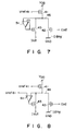
- Figs. 7 and 8 show modifications of the level conversion circuit 47 in the arrangement shown in Fig. 6.
- the same reference numerals in Figs. 7 and 8 denote the same parts as in the arrangement shown in Fig. 6, and a detailed description thereof will be omitted.
- the level conversion circuit 47 in the arrangement shown in Fig. 6 is constituted by an amplifier 51.
- the non-inverting input terminal of the amplifier 51 is connected to the node 46, and the inverting input terminal and the output terminal thereof are connected to the gate of the transistor 43.
- the drain of the transistor 43 is connected to the node 46, and the source thereof is connected to the current output terminal Iout.
- an amplifier 61 is arranged.
- the non-inverting input terminal of the amplifier 61 receives a predetermined reference voltage Vref61.
- the inverting input terminal of the amplifier 61 is connected to the node 46, and the output terminal thereof is connected to the gate of the transistor 43.
- the current paths can be switched at high speed, and a current mirror circuit, which can stably output a current to the terminal Iout, and has high precision, can be realized.
- a variable gate bias is applied upon switching of a current, thereby positively controlling the ON/OFF operation of a transistor.
- a switching constant current source circuit which can switch current paths at higher speed, and can perform a high-speed operation, can be provided.
Landscapes
- Analogue/Digital Conversion (AREA)
- Amplifiers (AREA)
- Electronic Switches (AREA)
- Control Of Electrical Variables (AREA)
- Logic Circuits (AREA)
Claims (1)
- Eine Schalt-Konstantstromquellenschaltung, umfassend:- einen ersten Strompfad (41, 46), um einen konstanten Strom zu versorgen;- einen ersten MOS-Transistor (42), wobei ein Ende eines seiner Strompfade mit dem ersten Strompfad (41, 46) verbunden ist, das andere Ende dieses Strompfades mit einem zweiten Strompfad (Idmy, GND) verbunden ist, und an dessen Gate ein digitales Signal (Cod) entsprechend einer logischen Amplitude angelegt ist;- einen zweiten MOS-Transistor (43), wobei ein Ende eines seiner Strompfade mit dem ersten Strompfad (41, 46) verbunden ist, das andere Ende dieses Strompfades mit einem dritten Strompfad (Iout) verbunden ist, und der einen Schaltbetrieb mit dem ersten MOS-Transistor (42) komplementär durchführt; und- einer Niveauumwandlungsvorrichtung (47), um eine Änderung der Spannung in dem ersten Strompfad (41, 46) zu holen, gemäß eines Betriebs des ersten MOS-Transistors (42) in Antwort auf das digitale Signal, und um alternativ ein erstes Niveau zum Aussetzen des zweiten MOS-Transistors (43), der komplementär mit dem ersten MOS-Transistor (42) arbeitet, und ein zweites Niveau zum Einsetzen des zweiten MOS-Transistors (43) zum Ausgeben eines vorherbestimmten Stromes anzulegen, worin- die Niveauumwandlungsschaltung (47) einen dritten MOS Transistor (45) einschließt, mit einem Tor mit dem ersten Strompfad (41, 46) verbunden, und einen vierten MOS Transistor (44), der mit dem dritten MOS Transistor (45) Kaskaden verbunden ist, wobei der den dritten und vierten MOS Transistor verbindende Knoten mit den Gates des vierten und zweiten MOS-Transistors verbunden ist.
Applications Claiming Priority (2)
| Application Number | Priority Date | Filing Date | Title |
|---|---|---|---|
| JP310871/90 | 1990-11-16 | ||
| JP2310871A JPH07112155B2 (ja) | 1990-11-16 | 1990-11-16 | スイッチング定電流源回路 |
Publications (3)
| Publication Number | Publication Date |
|---|---|
| EP0485973A2 EP0485973A2 (de) | 1992-05-20 |
| EP0485973A3 EP0485973A3 (en) | 1992-07-08 |
| EP0485973B1 true EP0485973B1 (de) | 1997-03-05 |
Family
ID=18010393
Family Applications (1)
| Application Number | Title | Priority Date | Filing Date |
|---|---|---|---|
| EP91119333A Expired - Lifetime EP0485973B1 (de) | 1990-11-16 | 1991-11-13 | Konstantstromquellen-Schaltkreis |
Country Status (5)
| Country | Link |
|---|---|
| US (1) | US5235218A (de) |
| EP (1) | EP0485973B1 (de) |
| JP (1) | JPH07112155B2 (de) |
| KR (1) | KR960010390B1 (de) |
| DE (1) | DE69124924T2 (de) |
Families Citing this family (15)
| Publication number | Priority date | Publication date | Assignee | Title |
|---|---|---|---|---|
| JPH0529845A (ja) * | 1991-07-25 | 1993-02-05 | Rohm Co Ltd | カレントミラー回路 |
| NL9201053A (nl) * | 1992-06-15 | 1994-01-03 | Koninkl Philips Electronics Nv | Switched capacitor ladingspomp, alsmede zaagtandoscillator voorzien van een dergelijke switched capacitor ladingspomp. |
| US5596286A (en) * | 1993-11-12 | 1997-01-21 | Texas Instruments Incorporated | Current limiting devices to reduce leakage, photo, or stand-by current in an integrated circuit |
| WO1995022093A1 (en) * | 1994-02-14 | 1995-08-17 | Philips Electronics N.V. | A reference circuit having a controlled temperature dependence |
| JP3519143B2 (ja) * | 1994-11-17 | 2004-04-12 | 三菱電機株式会社 | 電流型インバータ回路、電流型論理回路、電流型ラッチ回路、半導体集積回路、電流型リング発振器、電圧制御発振器及びpll回路 |
| US5798723A (en) * | 1996-07-19 | 1998-08-25 | National Semiconductor Corporation | Accurate and precise current matching for low voltage CMOS digital to analog converters |
| JP2001068948A (ja) * | 1999-08-27 | 2001-03-16 | Hitachi Kokusai Electric Inc | Mosfet増幅回路 |
| US6304121B1 (en) | 2000-04-05 | 2001-10-16 | Entridia Corporation | Process strength indicator |
| US6445223B1 (en) * | 2000-11-21 | 2002-09-03 | Intel Corporation | Line driver with an integrated termination |
| JP2003131031A (ja) | 2001-10-23 | 2003-05-08 | Dainippon Printing Co Ltd | 光学素子の製造方法および光学素子 |
| US6774683B2 (en) * | 2002-08-13 | 2004-08-10 | Analog Devices, Inc. | Control loop for minimal tailnode excursion of differential switches |
| JP4537840B2 (ja) * | 2004-12-13 | 2010-09-08 | 株式会社東芝 | 電流源セルおよびそれを用いたd/aコンバータ |
| JP4973243B2 (ja) * | 2007-03-06 | 2012-07-11 | 富士通セミコンダクター株式会社 | 半導体出力回路及び外部出力信号生成方法並びに半導体装置 |
| JP4408935B2 (ja) * | 2008-02-07 | 2010-02-03 | 日本テキサス・インスツルメンツ株式会社 | ドライバ回路 |
| WO2022197881A1 (en) * | 2021-03-18 | 2022-09-22 | Texas Instruments Incorporated | A compensated digital-to-analog converter (dac) |
Family Cites Families (7)
| Publication number | Priority date | Publication date | Assignee | Title |
|---|---|---|---|---|
| US4495425A (en) * | 1982-06-24 | 1985-01-22 | Motorola, Inc. | VBE Voltage reference circuit |
| EP0262480B1 (de) * | 1986-09-24 | 1991-08-07 | Siemens Aktiengesellschaft | Stromspiegel-Schaltungsanordnung |
| GB2206010A (en) * | 1987-06-08 | 1988-12-21 | Philips Electronic Associated | Differential amplifier and current sensing circuit including such an amplifier |
| EP0356570A1 (de) * | 1988-09-02 | 1990-03-07 | Siemens Aktiengesellschaft | Stromspiegel |
| US4928056A (en) * | 1988-10-06 | 1990-05-22 | National Semiconductor Corporation | Stabilized low dropout voltage regulator circuit |
| GB8913439D0 (en) * | 1989-06-12 | 1989-08-02 | Inmos Ltd | Current mirror circuit |
| US5124632A (en) * | 1991-07-01 | 1992-06-23 | Motorola, Inc. | Low-voltage precision current generator |
-
1990
- 1990-11-16 JP JP2310871A patent/JPH07112155B2/ja not_active Expired - Fee Related
-
1991
- 1991-11-11 KR KR1019910019962A patent/KR960010390B1/ko not_active Expired - Fee Related
- 1991-11-13 DE DE69124924T patent/DE69124924T2/de not_active Expired - Fee Related
- 1991-11-13 EP EP91119333A patent/EP0485973B1/de not_active Expired - Lifetime
- 1991-11-14 US US07/791,379 patent/US5235218A/en not_active Expired - Fee Related
Also Published As
| Publication number | Publication date |
|---|---|
| EP0485973A2 (de) | 1992-05-20 |
| JPH07112155B2 (ja) | 1995-11-29 |
| KR960010390B1 (ko) | 1996-07-31 |
| EP0485973A3 (en) | 1992-07-08 |
| DE69124924D1 (de) | 1997-04-10 |
| US5235218A (en) | 1993-08-10 |
| JPH04181817A (ja) | 1992-06-29 |
| DE69124924T2 (de) | 1997-07-24 |
| KR920011039A (ko) | 1992-06-27 |
Similar Documents
| Publication | Publication Date | Title |
|---|---|---|
| US4752703A (en) | Current source polarity switching circuit | |
| US5235218A (en) | Switching constant current source circuit | |
| US4394587A (en) | CMOS Differential comparator with hysteresis | |
| US5463394A (en) | Current switch for a high speed DAC | |
| US5334883A (en) | Circuit for introducing hysterisis | |
| JPH05145384A (ja) | Cmosレシーバ入力インターフエース回路 | |
| JPH0744438B2 (ja) | 遅延回路 | |
| KR970023370A (ko) | 기준전류 발생회로 | |
| US5362994A (en) | Comparator with controlled hysteresis | |
| JP2885177B2 (ja) | 電源モニタ回路 | |
| EP1001535B1 (de) | Schaltung zum Steuern der Änderungsgeschwindigkeit der Ausgangsspannung eines Treibers in Gegentakt-Konfiguration | |
| US5218364A (en) | D/a converter with variable biasing resistor | |
| US4868421A (en) | Bimos circuit that provides low power dissipation and high transient drive capability | |
| JPH082019B2 (ja) | レベル変換回路 | |
| US5706006A (en) | Operational amplifier incorporating current matrix type digital-to-analog converter | |
| JPH1188159A (ja) | チャ−ジポンプ回路 | |
| US6278322B1 (en) | Transconductance amplifier and automatic gain control device using it | |
| US20030160599A1 (en) | Controllable Current Source Assembly | |
| US6147541A (en) | Monolithic MOS-SC circuit | |
| US6130569A (en) | Method and apparatus for a controlled transition rate driver | |
| JP3370169B2 (ja) | 出力回路 | |
| US6798263B1 (en) | Reset feature for a low voltage differential latch | |
| US5831465A (en) | Variable delay circuit | |
| JP3859883B2 (ja) | 電流源回路および電圧発生回路 | |
| EP0320779B1 (de) | Abfühlverstärker |
Legal Events
| Date | Code | Title | Description |
|---|---|---|---|
| PUAI | Public reference made under article 153(3) epc to a published international application that has entered the european phase |
Free format text: ORIGINAL CODE: 0009012 |
|
| 17P | Request for examination filed |
Effective date: 19911113 |
|
| AK | Designated contracting states |
Kind code of ref document: A2 Designated state(s): DE FR GB |
|
| PUAL | Search report despatched |
Free format text: ORIGINAL CODE: 0009013 |
|
| AK | Designated contracting states |
Kind code of ref document: A3 Designated state(s): DE FR GB |
|
| 17Q | First examination report despatched |
Effective date: 19950518 |
|
| GRAG | Despatch of communication of intention to grant |
Free format text: ORIGINAL CODE: EPIDOS AGRA |
|
| GRAH | Despatch of communication of intention to grant a patent |
Free format text: ORIGINAL CODE: EPIDOS IGRA |
|
| GRAH | Despatch of communication of intention to grant a patent |
Free format text: ORIGINAL CODE: EPIDOS IGRA |
|
| GRAA | (expected) grant |
Free format text: ORIGINAL CODE: 0009210 |
|
| AK | Designated contracting states |
Kind code of ref document: B1 Designated state(s): DE FR GB |
|
| REF | Corresponds to: |
Ref document number: 69124924 Country of ref document: DE Date of ref document: 19970410 |
|
| ET | Fr: translation filed | ||
| PGFP | Annual fee paid to national office [announced via postgrant information from national office to epo] |
Ref country code: GB Payment date: 19971104 Year of fee payment: 7 |
|
| PGFP | Annual fee paid to national office [announced via postgrant information from national office to epo] |
Ref country code: DE Payment date: 19971121 Year of fee payment: 7 |
|
| PLBE | No opposition filed within time limit |
Free format text: ORIGINAL CODE: 0009261 |
|
| STAA | Information on the status of an ep patent application or granted ep patent |
Free format text: STATUS: NO OPPOSITION FILED WITHIN TIME LIMIT |
|
| 26N | No opposition filed | ||
| PG25 | Lapsed in a contracting state [announced via postgrant information from national office to epo] |
Ref country code: GB Free format text: LAPSE BECAUSE OF NON-PAYMENT OF DUE FEES Effective date: 19981113 |
|
| GBPC | Gb: european patent ceased through non-payment of renewal fee |
Effective date: 19981113 |
|
| PG25 | Lapsed in a contracting state [announced via postgrant information from national office to epo] |
Ref country code: DE Free format text: LAPSE BECAUSE OF NON-PAYMENT OF DUE FEES Effective date: 19990901 |
|
| PGFP | Annual fee paid to national office [announced via postgrant information from national office to epo] |
Ref country code: FR Payment date: 20041109 Year of fee payment: 14 |
|
| PG25 | Lapsed in a contracting state [announced via postgrant information from national office to epo] |
Ref country code: FR Free format text: LAPSE BECAUSE OF NON-PAYMENT OF DUE FEES Effective date: 20060731 |
|
| REG | Reference to a national code |
Ref country code: FR Ref legal event code: ST Effective date: 20060731 |