EP0486049A2 - Entscheidungsrückgekoppelter Entzerrer - Google Patents
Entscheidungsrückgekoppelter Entzerrer Download PDFInfo
- Publication number
- EP0486049A2 EP0486049A2 EP91119532A EP91119532A EP0486049A2 EP 0486049 A2 EP0486049 A2 EP 0486049A2 EP 91119532 A EP91119532 A EP 91119532A EP 91119532 A EP91119532 A EP 91119532A EP 0486049 A2 EP0486049 A2 EP 0486049A2
- Authority
- EP
- European Patent Office
- Prior art keywords
- signal
- equalizer
- decision
- feedback equalizer
- decision feedback
- Prior art date
- Legal status (The legal status is an assumption and is not a legal conclusion. Google has not performed a legal analysis and makes no representation as to the accuracy of the status listed.)
- Granted
Links
Images


Classifications
-
- H—ELECTRICITY
- H04—ELECTRIC COMMUNICATION TECHNIQUE
- H04L—TRANSMISSION OF DIGITAL INFORMATION, e.g. TELEGRAPHIC COMMUNICATION
- H04L25/00—Baseband systems
- H04L25/02—Details ; arrangements for supplying electrical power along data transmission lines
- H04L25/03—Shaping networks in transmitter or receiver, e.g. adaptive shaping networks
- H04L25/03006—Arrangements for removing intersymbol interference
- H04L25/03012—Arrangements for removing intersymbol interference operating in the time domain
- H04L25/03019—Arrangements for removing intersymbol interference operating in the time domain adaptive, i.e. capable of adjustment during data reception
- H04L25/03057—Arrangements for removing intersymbol interference operating in the time domain adaptive, i.e. capable of adjustment during data reception with a recursive structure
Definitions
- the present invention relates to a decision feedback equalizer and, more particularly, to a decision feedback equalizer to be used at a receiving station in a digital radio communication system which uses multilevel quadrature amplitude modulation or multiphase phase modulation.
- a receiving station uses a transversal equalizer with a transversal filter in order to overcome the degradation of a channel ascribable to frequency-selective fading which occurs on a transmission path.
- a decision feedback equalizer is even superior to such an equalizer regarding the equalizing characteristic.
- a decision feedback equalizer is disclosed by D.A. George et al in "An Adaptive Decision Feedback Equalizer", IEEE TRANSACTIONS ON COMMUNICATION TECHNOLOGY, Vol. COM-l9, No. 3 June l97l, pp. 28l-293.
- the level of a baseband signal being outputted by a demodulator sometimes becomes higher than a predetermined level. Then, the frequency characteristic inside the band noticeably varies and, in the worst case, exceeds the predetermined input range of an analog-to-digital (A/D) converter which follows the demodulator, preventing a received signal from being adequately equalized.
- A/D analog-to-digital
- an object of the present invention to provide a decision feedback equalizer capable of equalizing a received signal even when an interference wave of substantially the same level as a principal wave is generated.
- a decision feedback equalizer for equalizing the output of a demodulator of the present invention comprises a gain control circuit for amplitude-compressing an n-level analog baseband signal fed from the demodulator to l/K (K ⁇ l) and outputting the amplitude-compressed signal.
- An A/D converter samples the compressed signal and outputs the sampled signal.
- a decision feedback transversal filter has a feedforward equalizer, a feedback equalizer, and an adder for adding the outputs of the feedforward and feedback equalizers. The decision feedback transversal filter receives the sampled signal and a signal undergone expansion and decision at the preceding equalizer and succeeding equalizer, respectively, and executes equalization by using tap coefficients to output an equalized digital signal sequence.
- An expansion and decision circuit expands the equalized digital signal sequence by L times (L > l) and discriminates the expanded signal sequence to produce the signal undergone expansion and decision.
- a postporcessor expands the equalized digital signal sequence by K times and discriminates the expanded signal sequence to output a data signal including a polarity signal, and an error signal.
- a control signal generator generates the tap coefficients.
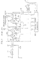
- the conventional decision feedback equalizer has a full digital 5-tap configuration.
- An analog baseband signal from a demodulator, not shown, is applied to a gain control circuit (GCC) ll via a data input terminal l.
- GCC gain control circuit
- the output of the GCC ll is connected to the input of an A/D converter 12 which has a predetermined input range.
- the GCC ll compresses the amplitude of the analog baseband signal to l/K (K ⁇ l) and applies the amplitude-compressed signal to the A/D converter l2, so that the amplitude-compressed signal may not exceed the input range of the A/D converter l2 when waveform distortions occur due to fading on the transmission path.
- a clock signal CLK is fed to the A/D converter l2 via a clock input terminal 2.
- the A/D converter 12 samples the amplitude-compressed signal at a sampling frequency f c and delivers the sampled signal to a decision feedback transversal filter l0l as an N-bit digital signal sequence Sl.
- the decision feedback transversal filter l0l has a feedforward equalizer 20l and a feedback equalizer 202.
- the digital signal sequence Sl is fed to a first multiplier 25 and a first delay circuit 2l.
- the output of the first delay circuit 2l is connected to a second multiplier 26 and a second delay circuit 22.
- the output of the second delay circuit 22 is connected to a third multiplier 27.
- a decision circuit l4 descriminates the output Sl' of the transversal filter l0l and delivers the resulting output thereof to the feedback equalizer 202.
- the output of the decision circuit l4 is applied to a third delay circuit 23 whose output is connected to a fourth multiplier 28 and a fourth delay circuit 24.
- the output of the fourth delay circuit 24 is connected to a fifth multiplier 29.
- the delay circuits 2l - 24 are each implemented by, for example, a D-type flip-flop for delaying the input by l/f c .
- the multipliers 25 - 29 multiply respectively their input digital signals by tap coefficients C ⁇ 2, C -l , C0, C l and C2 which are fed thereto from a control signal generator l02.
- the resulting outputs m ⁇ 2, m -l , m0, m l and m2 of the multipliers 25 - 29, respectively, are fed to an adder l3.
- the adder l3 digitally adds the inputs m ⁇ 2 - m2 to thereby remove intersymbol interference included in the original signal Sl.
- the output of the adder l3, i.e., equalized digital signal sequence Sl' is delivered to a postprocessor l5 and the decision circuit l4.
- the decision circuit l4 which will be described in detail later, determines the input signal level (binary number) to be an ideal signal level closest thereto and delivers the result of decision as a decision signal.
- the succedding equalizer 202 consisting of the delay circuits 23 and 24 and multipliers 28 and 29 receives the decision signal which is free from the waveform distortions ascribable to fading or similar cause.
- the postprocessor l5 restores the original signal having been compressed to l/K by the GCC ll to the original level, i.e., to the level which would be obtainable if the non-amplitude-compressed signal were applied to the decision feedback equalizer.
- the signal whose level is so corrected by the postprocessor l5 is sent out as an output signal d of the equalizer via an output terminal 3. Further, the postprocessor l5 delivers to the control signal generator l02 a discrimination error signal e representative of a difference between the equalized signal and the ideal value.
- the input signal to the data input terminal l is the in-phase or orthogonal baseband signal (4-level) undergone 16-level quadrature amplitude modulation (l6 QAM).
- the 4-level signal would have ideal levels A, B, C and D as indicated by circles in FIG. 2A.
- the ideal levels A, B, C and D are respectively representative of 2-bit data signals (00), (0l), (l0) and (ll) of the first and second bits.
- the third bit and successive bits shown in FIG. 2A are representative of deviations from the ideal values, i.e., discrimination error signals.
- the points A, B, C and D are compressed to points A', B', C' and D' as indicated by dots in FIG. 2A.
- the ideal values of the points A', B', C' and D' are represented by 3-bit signals (0l0), (0ll), (l00) and (l0l), respectively.
- the fourth bit and successive bits constitute the discrimination error signal. Since the output signal Sl' of the decision feedback transversal filter l0l include thermal noise and intersymbol interference which is unable to be removed, the discrimination error signal varies randomly. Therefore, should the first to N-th bit signals be directly fed back to the feedback equalizer 202, the error included in the input to the equalizer would disturb equalization.
- the postprocessor l5 doubles the compressed signal to restore it to the original signal level obtainable if the signal were not compressed, by executing signal conversion as shown in FIG. 2C.
- the postprocessor l5 outputs a signal having three bits which are associated with paths l, 2 and 3, respectively.
- the paths l and 2 are the data bits d while the path 3 is the error bit e showing the polarity of an error signal.
- the control signal generator l02 determines the correlation between the polarity signals d (path l) and the error signals e (path 3) to output the tap coefficients C ⁇ 2 - C2 as mean values with respect to time.
- This kind of principle of tap coefficient generation belongs to a family of conventional adaptive automatic equalization algorithms and taught in, for example, "DIGITAL SIGNAL PROCESSING", The Institute of Electronics and Communication Engineers of Japan, l975, Chapter ll.
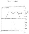
- FIG. 3 shows a two wave interference fading equalization characteristic particular to the above-described conventional decision feedback equalizer and sometimes called a signature curve.
- the abscissa indicates notch positions ⁇ f d produced by normalizing the deviations of the notch frequencies of fading from the center of the spectrum by a clock frequency; the ordinate indicates amplitude ratios ⁇ produced by normalizing the amplitudes of reflected waves (delayed waves) by the amplitude of a principal wave.
- ⁇ and T denote respectively a time lag between the principal and delayed waves and an intersymbol distance l/f c .
- the input signal to the feedback equalizer 202 is the decision signal undergone equalization and, therefore, substantially identical with an ideal value, Therefore, in the range of 0 ⁇ ⁇ ⁇ l shown in FIG. 3, the decision feedback equalizer executes substantially perfect equalization.
- the equalizing ability is poorer than in the case of 0 ⁇ ⁇ ⁇ l since the input to the feedforward equalizer 20l still contains intersymbol interference.
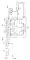
- FIG. 4 a decision feedback equalizer embodying the present invention is shown which is free from the drawback particular to the conventional equalizer as discussed above.
- the embodiment has an expansion and decision circuit l04 in place of the decision circuit l4.
- the embodiment is similar to the conventional technology shown in FIG. l. Hence, let the following description concentrate on the expansion and decision circuit l04.
- the conventional equalizer applies the decision output of the decision circuit l4 which has been compressed to l/K to the input of the multipliers.
- the expansion and decision circuit l04 expands the amplitude of decision output by L (L > l) times and feeds the resulting expanded decision output to the multipliers 28 and 29 via the delay circuits 23 and 24.
- multipliers 28 and 29 each outputs an L times greater product to thereby noticeably enhance the equalizing ability, compared to the conventional decision feedback equalizer.
- the embodiment is capable of equalizing a received signal even with greater amplitude ratios ⁇ than the conventional decision feedback equalizer (presented by a dotted line).
- the expansion and decision circuit l4 outputs, for example, (00l00 ... 0) in response to a signal A' or outputs (l0l00 ... 0) for a signal C'.
- n is the number of levels of an input analog baseband signal and is, for example, 4 when the input analog baseband signal is a l6 QAM in-phase component.
- T i (l/2K) ⁇ (a i + a i+l ).
- Sl' smaller than T l and Sl' greater than T n-l be(L/K) ⁇ a l and(L/K) ⁇ a n , respectively.
- Table l The relation between the input signal Sl' and the expansion and decision circuit output signal Sl'' is shown in Table l below.
- the expansion and decision circuit l4 can be implemented easily and economically by a ROM (Read Only Memory) or similar memory and a logic circuit including an AND gate and an OR gate.
- the decision feedback transversal filter section can be implemented by multipliers having the same number of input and output bits as conventional multipliers, eliminating the need for a greater number of coefficient bits or a greater number of output bits.
- K has to have a great value since the input level of the A/D converter l2 is restricted by the waveform distortions.
- the illustrative embodiment allows L to be increased in proportion to K, further enhancing the equalizing ability. Specifically, as K is increased to accommodate greater waveform distortions, L can be increased also and allows much more greater waveform distortions to be equalized.
- L greater than K may be selected to further enhance the equalizing ability.
- the succeeding equalizer 202 may be used if the delay circuit 23 is omitted therefrom.
- the control signal generator l02 is supplied the polarity signal (first bit of d) in the output of the postprocessor l5.
- the polarity signal may be replaced with a polarity signal which is the first bit of the feedforward equalizer 20l input (d').
- the polarity signal may be replaced with a polarity signal, FIG. 8, which is the first bit of the adder l3 output (d'').
- use may be made of a data signal including not only the polarity (first bit) but also the second bit and successive bits.
- the present invention has been shown and described in relation to a unidimensional 5-tap decision feedback equalizer, the present invention is of course practicable with any other desired number of taps. Moreover, the present invention is applicable to an orthogonal 2-dimensional equalizer having four cascaded equalizer sections particular to QAM or multiphase phase modulation.
- the present invention provides a decision feedback equalizer which has a greater equalizing ability than a conventional equalizer of this type.
- an expansion and decision circuit is connected between the output of a decision feedback transversal filter section and the decision feedback input of a feedback equalizer so as to expand the signal level to be fed back.
Landscapes
- Engineering & Computer Science (AREA)
- Power Engineering (AREA)
- Computer Networks & Wireless Communication (AREA)
- Signal Processing (AREA)
- Cable Transmission Systems, Equalization Of Radio And Reduction Of Echo (AREA)
- Filters That Use Time-Delay Elements (AREA)
Applications Claiming Priority (3)
| Application Number | Priority Date | Filing Date | Title |
|---|---|---|---|
| JP2308827A JP2551231B2 (ja) | 1990-11-16 | 1990-11-16 | 判定帰還形等化器 |
| JP308827/90 | 1990-11-16 | ||
| CA002055847A CA2055847C (en) | 1990-11-16 | 1991-11-19 | Decision feedback equalizer |
Publications (3)
| Publication Number | Publication Date |
|---|---|
| EP0486049A2 true EP0486049A2 (de) | 1992-05-20 |
| EP0486049A3 EP0486049A3 (en) | 1992-11-25 |
| EP0486049B1 EP0486049B1 (de) | 1996-08-28 |
Family
ID=25674862
Family Applications (1)
| Application Number | Title | Priority Date | Filing Date |
|---|---|---|---|
| EP91119532A Expired - Lifetime EP0486049B1 (de) | 1990-11-16 | 1991-11-15 | Entscheidungsrückgekoppelter Entzerrer |
Country Status (5)
| Country | Link |
|---|---|
| US (1) | US5267265A (de) |
| EP (1) | EP0486049B1 (de) |
| JP (1) | JP2551231B2 (de) |
| AU (1) | AU639618B2 (de) |
| CA (1) | CA2055847C (de) |
Families Citing this family (18)
| Publication number | Priority date | Publication date | Assignee | Title |
|---|---|---|---|---|
| JP2551231B2 (ja) | 1990-11-16 | 1996-11-06 | 日本電気株式会社 | 判定帰還形等化器 |
| JPH0563605A (ja) * | 1991-08-30 | 1993-03-12 | Nec Corp | 適応型最尤系列推定受信器 |
| DE69228649T2 (de) * | 1991-11-18 | 1999-08-12 | Nec Corp., Tokio/Tokyo | Automatischer Entzerrer zur wirkungsvollen Kompensation der Nachbarsymbolinterferenz und der Kreuzpolarisationsinterferenz bei einer doppelten Gleichkanalpolarisation |
| JP2720721B2 (ja) * | 1992-08-21 | 1998-03-04 | 日本電気株式会社 | 変復調装置 |
| US5517527A (en) * | 1992-12-11 | 1996-05-14 | Industrial Technology Research Institute | Adaptive equalizer for ISDN U-interface transceiver |
| US5539774A (en) * | 1994-06-15 | 1996-07-23 | International Business Machines Corporation | Dual decision equalization method and device |
| JP3400545B2 (ja) * | 1994-06-23 | 2003-04-28 | 株式会社日立製作所 | 判定帰還型等化器 |
| US5930296A (en) * | 1997-04-08 | 1999-07-27 | Glenayre Electronics, Inc. | Low-complexity bidirectional equalizer |
| US6240133B1 (en) * | 1998-02-05 | 2001-05-29 | Texas Instruments Incorporated | High stability fast tracking adaptive equalizer for use with time varying communication channels |
| JP2001345743A (ja) * | 2000-06-06 | 2001-12-14 | Iwatsu Electric Co Ltd | 判定帰還型等化器 |
| US7027504B2 (en) * | 2001-09-18 | 2006-04-11 | Broadcom Corporation | Fast computation of decision feedback equalizer coefficients |
| EP1587265A1 (de) * | 2004-01-15 | 2005-10-19 | Alcatel | Erfassung von Fehlerausbreitung bei entscheidungsrückgekoppelter Entzerrung |
| US7483479B2 (en) | 2004-09-16 | 2009-01-27 | Keyeye Communications | Scaled signal processing elements for reduced filter tap noise |
| EP2375662B1 (de) * | 2005-01-20 | 2018-09-26 | Rambus Inc. | Hochgeschwindigkeitssignalsysteme mit anpassbarer präemphase und entzerrung |
| US8341506B2 (en) * | 2007-03-30 | 2012-12-25 | HGST Netherlands B.V. | Techniques for correcting errors using iterative decoding |
| US10940092B2 (en) | 2017-04-19 | 2021-03-09 | Michael Moonsup Song | Technologies for medicine dispensing |
| CN109769255B (zh) * | 2018-12-21 | 2020-11-06 | 京信通信系统(中国)有限公司 | 数据压缩方法、装置、计算机设备和存储介质 |
| JP7325902B2 (ja) * | 2019-07-04 | 2023-08-15 | 日本無線株式会社 | 判定帰還型等化器および受信機 |
Family Cites Families (5)
| Publication number | Priority date | Publication date | Assignee | Title |
|---|---|---|---|---|
| DE3000856A1 (de) * | 1980-01-11 | 1981-07-16 | Licentia Patent-Verwaltungs-Gmbh, 6000 Frankfurt | Adaptive entzerrereinrichtung |
| US4524424A (en) * | 1982-02-18 | 1985-06-18 | Rockwell International Corporation | Adaptive spectrum shaping filter |
| IT1188626B (it) * | 1986-03-25 | 1988-01-20 | Gte Telecom Spa | Metodo e dispositivo di equalizzazione adattiva cieca |
| JPH03154435A (ja) * | 1989-11-13 | 1991-07-02 | Toshiba Corp | 判定帰還形等化方式 |
| JP2551231B2 (ja) | 1990-11-16 | 1996-11-06 | 日本電気株式会社 | 判定帰還形等化器 |
-
1990
- 1990-11-16 JP JP2308827A patent/JP2551231B2/ja not_active Expired - Lifetime
-
1991
- 1991-11-15 US US07/792,795 patent/US5267265A/en not_active Expired - Lifetime
- 1991-11-15 EP EP91119532A patent/EP0486049B1/de not_active Expired - Lifetime
- 1991-11-18 AU AU87950/91A patent/AU639618B2/en not_active Expired
- 1991-11-19 CA CA002055847A patent/CA2055847C/en not_active Expired - Lifetime
Also Published As
| Publication number | Publication date |
|---|---|
| AU8795091A (en) | 1992-05-21 |
| JP2551231B2 (ja) | 1996-11-06 |
| JPH04181802A (ja) | 1992-06-29 |
| EP0486049A3 (en) | 1992-11-25 |
| US5267265A (en) | 1993-11-30 |
| AU639618B2 (en) | 1993-07-29 |
| CA2055847A1 (en) | 1993-05-20 |
| EP0486049B1 (de) | 1996-08-28 |
| CA2055847C (en) | 1995-11-28 |
Similar Documents
| Publication | Publication Date | Title |
|---|---|---|
| EP0486049B1 (de) | Entscheidungsrückgekoppelter Entzerrer | |
| US5353306A (en) | Tap-weight controller for adaptive matched filter receiver | |
| US7272177B2 (en) | Demodulation apparatus for a network transceiver and method thereof | |
| US5191598A (en) | System for reducing the affects of signal fading on received signals | |
| JP2715662B2 (ja) | 時分割信号のダイバーシチ受信のための方法および装置 | |
| US6510188B1 (en) | All digital automatic gain control circuit | |
| EP0609828A2 (de) | Adaptiver, signalangepasster Filter | |
| US6205170B1 (en) | Transmission/reception unit with bidirectional equalization | |
| EP0216183A2 (de) | Entscheidungsrückgekoppelter Entzerrer mit Musterdetektor | |
| US5321723A (en) | Automatic equalizer | |
| US7184504B2 (en) | Receiver having an integrated clock phase detector | |
| JP3099831B2 (ja) | 自動等化器 | |
| US6175591B1 (en) | Radio receiving apparatus | |
| JPH0575498A (ja) | 判定帰還形自動等化器 | |
| EP0155048A1 (de) | Datenübertragungssystem | |
| US4809298A (en) | Radio data transmission system | |
| JP2616152B2 (ja) | 自動等化器 | |
| US5442582A (en) | Transversal filter allrate equalizer for use at intermediate frequency | |
| WO1991017607A1 (en) | A method of equalization in a receiver of signals having passed a transmission channel | |
| US5530721A (en) | Equalizer and terminal device for mobile communications | |
| JPH0310425A (ja) | トランスバーサルフィルタ制御回路 | |
| US12407546B2 (en) | Decision-feedback equalizer using feedback filter with controllable delay circuit and associated method | |
| JP2827197B2 (ja) | 無線データ伝送システム | |
| JPH05130152A (ja) | 自動等化器 | |
| EP0237287A2 (de) | Transversalentzerreranordnungen |
Legal Events
| Date | Code | Title | Description |
|---|---|---|---|
| PUAI | Public reference made under article 153(3) epc to a published international application that has entered the european phase |
Free format text: ORIGINAL CODE: 0009012 |
|
| 17P | Request for examination filed |
Effective date: 19911211 |
|
| AK | Designated contracting states |
Kind code of ref document: A2 Designated state(s): BE DE FR GB IT NL |
|
| PUAL | Search report despatched |
Free format text: ORIGINAL CODE: 0009013 |
|
| AK | Designated contracting states |
Kind code of ref document: A3 Designated state(s): BE DE FR GB IT NL |
|
| 17Q | First examination report despatched |
Effective date: 19950313 |
|
| GRAH | Despatch of communication of intention to grant a patent |
Free format text: ORIGINAL CODE: EPIDOS IGRA |
|
| GRAA | (expected) grant |
Free format text: ORIGINAL CODE: 0009210 |
|
| GRAH | Despatch of communication of intention to grant a patent |
Free format text: ORIGINAL CODE: EPIDOS IGRA |
|
| AK | Designated contracting states |
Kind code of ref document: B1 Designated state(s): BE DE FR GB IT NL |
|
| REF | Corresponds to: |
Ref document number: 69121671 Country of ref document: DE Date of ref document: 19961002 |
|
| ET | Fr: translation filed | ||
| ITF | It: translation for a ep patent filed | ||
| PLBE | No opposition filed within time limit |
Free format text: ORIGINAL CODE: 0009261 |
|
| STAA | Information on the status of an ep patent application or granted ep patent |
Free format text: STATUS: NO OPPOSITION FILED WITHIN TIME LIMIT |
|
| 26N | No opposition filed | ||
| REG | Reference to a national code |
Ref country code: GB Ref legal event code: IF02 |
|
| PGFP | Annual fee paid to national office [announced via postgrant information from national office to epo] |
Ref country code: NL Payment date: 20101116 Year of fee payment: 20 Ref country code: FR Payment date: 20101123 Year of fee payment: 20 |
|
| PGFP | Annual fee paid to national office [announced via postgrant information from national office to epo] |
Ref country code: DE Payment date: 20101110 Year of fee payment: 20 |
|
| PGFP | Annual fee paid to national office [announced via postgrant information from national office to epo] |
Ref country code: GB Payment date: 20101110 Year of fee payment: 20 Ref country code: BE Payment date: 20101020 Year of fee payment: 20 Ref country code: IT Payment date: 20101120 Year of fee payment: 20 |
|
| REG | Reference to a national code |
Ref country code: DE Ref legal event code: R071 Ref document number: 69121671 Country of ref document: DE |
|
| REG | Reference to a national code |
Ref country code: DE Ref legal event code: R071 Ref document number: 69121671 Country of ref document: DE |
|
| REG | Reference to a national code |
Ref country code: NL Ref legal event code: V4 Effective date: 20111115 |
|
| BE20 | Be: patent expired |
Owner name: *NEC CORP. Effective date: 20111115 |
|
| REG | Reference to a national code |
Ref country code: GB Ref legal event code: PE20 Expiry date: 20111114 |
|
| PG25 | Lapsed in a contracting state [announced via postgrant information from national office to epo] |
Ref country code: NL Free format text: LAPSE BECAUSE OF EXPIRATION OF PROTECTION Effective date: 20111115 |
|
| PG25 | Lapsed in a contracting state [announced via postgrant information from national office to epo] |
Ref country code: GB Free format text: LAPSE BECAUSE OF EXPIRATION OF PROTECTION Effective date: 20111114 |
|
| PG25 | Lapsed in a contracting state [announced via postgrant information from national office to epo] |
Ref country code: DE Free format text: LAPSE BECAUSE OF EXPIRATION OF PROTECTION Effective date: 20111116 |