EP0486195A2 - Graphisches Rechnersystem - Google Patents
Graphisches Rechnersystem Download PDFInfo
- Publication number
- EP0486195A2 EP0486195A2 EP91310161A EP91310161A EP0486195A2 EP 0486195 A2 EP0486195 A2 EP 0486195A2 EP 91310161 A EP91310161 A EP 91310161A EP 91310161 A EP91310161 A EP 91310161A EP 0486195 A2 EP0486195 A2 EP 0486195A2
- Authority
- EP
- European Patent Office
- Prior art keywords
- line
- data
- bitblt
- triangle
- address conversion
- Prior art date
- Legal status (The legal status is an assumption and is not a legal conclusion. Google has not performed a legal analysis and makes no representation as to the accuracy of the status listed.)
- Withdrawn
Links
Images


Classifications
-
- G—PHYSICS
- G06—COMPUTING OR CALCULATING; COUNTING
- G06T—IMAGE DATA PROCESSING OR GENERATION, IN GENERAL
- G06T15/00—Three-dimensional [3D] image rendering
- G06T15/50—Lighting effects
- G06T15/80—Shading
- G06T15/87—Gouraud shading
-
- G—PHYSICS
- G06—COMPUTING OR CALCULATING; COUNTING
- G06T—IMAGE DATA PROCESSING OR GENERATION, IN GENERAL
- G06T15/00—Three-dimensional [3D] image rendering
- G06T15/50—Lighting effects
- G06T15/80—Shading
- G06T15/83—Phong shading
Definitions
- the present invention relates generally to computer graphics systems and more specifically to a high performance rasterization processor for such a system.
- a primary requirement for an effective computer graphics system is an ability to process large amounts of data activity to process large amounts of data defining images to be displayed on a screen in the form of many thousands of picture elements or pixels. As images change, the data requires updating at high speed, putting considerable demands on the processing resources available.
- a computer graphics system for rendering lines on a display comprising a plurality of processors coupled in series, each processor being arranged to perform a sequential portion of a Bresenham line draw algorithm.
- a method of rendering lines in a computer graphics system comprising the steps of sequentially computing address conversion data in a first processor and, upon receiving the address conversion data, computing pixel location data from said address conversion data in a second processor.
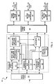
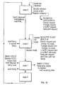
- graphics card 200 includes a front end graphics processor 210, a rasterization processor and display controller 220 (also known as a rasterizer or a rasterization engine), a frame buffer 230, a Z buffer 240, an attribute buffer 250, and a RAMDAC 260.
- the frame buffer and the attribute buffer are usually VRAM and the Z buffer is usually DRAM.
- the front end graphics processor 210 receives instructions from the main processor regarding a graphics construct or image in world coordinates and described generally by what are called image primitives which include triangles, bitblts, lines, etc.
- the front end graphics processor can also handle pixel instructions from the workstation processor.
- the front end graphics processor then performs various transformation, clipping and lighting instructions thereby describing the graphics construct or image in near screen coordinates. This information is then passed on to rasterizer 220.
- the frame buffer 230 which may be double buffered, includes a description of the red, green and blue colours for each pixel of the graphics display.
- the Z buffer contains a description of the depth or Z value of the pixels stored in the frame buffer. This information is useful for the rasterizer to determine whether or not a proposed pixel to be displayed based on a logical test. If the logical test is false, then the frame and Z buffers are not updated and the current pixel is displayed rather than the proposed pixel. If the logical test is true, then the frame and Z buffers are updated and the proposed pixel is displayed.
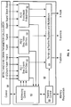
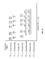
- Fig. 2 is a block diagram of rasterization processor 220.
- An input interface 300 communicates with the front end graphics processor in a predetermined protocol. Based on this communication, the input interface decodes addresses, directs data to the appropriate internal registers, and generates interface timings which meet a rasterizer front end 305's requirements. For example, the input interface sends information pertaining to triangle primitives to a triangle interpolator 310. In addition, the input interface sends the address information of bitblt and line primitives to a bitblt and line draw parameter calculator 320 and the corresponding data to a width and format convertor 330. In the preferred embodiment, the input interface determines if the internal registers are free to receive data.
- the input interface write protects the internal registers and holds up the data until the appropriate internal registers are free to receive the data.
- the input interface read protects internal registers that do not have valid data.
- the input interface has two-way communication, including status information, with a command interpreter and supervisor 340.
- the input interface also passes certain CRT control codes to a CRT controller 350.
- Triangle interpolator 310 can be viewed as an address and data splitter. Information pertaining to triangle primitives are sent to the triangle interpolator 310, which the triangle interpolator then separates into a series of line primitives. The triangle interpolator then splits the address information from the data for the line primitives and passes the address information to the bitblt and line draw parameter calculator. The triangle interpolator also passes the corresponding data (including colour and information) to a data path 370 in the appropriate width and format. The triangle interpolator can also handle trapezoid primitives (quadrilaterals that have upper and lower edges that are parallel to the X axis) in a similar manner.
- Bitblt and line draw parameter calculator 320 receives the address information of horizontal line primitives from triangle interpolator 310 and the address information of bitblt and line primitives in any orientation from the graphics processor via input interface 300.
- the bitblt and line draw parameter calculator then calculates various parameters for the bitblt and line primitives and passes that information to a bitblt and line draw sequencer 360.
- the bitblt and line draw sequencer then generates incremental pixel addresses for every pixel affected by the bitblt or line primitive.
- the sequencer also provides controlling information to data path 370. This information is then passed on to a hierarchical memory controller 380 (also referred to as a memory hypervisor) to update the frame buffer and the Z buffer.
- a hierarchical memory controller 380 also referred to as a memory hypervisor
- the triangle interpolator can be viewed as an address and data splitter.
- a Gouraud shaded triangle can be rendered by slicing the triangle primitive into horizontal lines, interpolating along the left edge to calculate the XY values and colours for each line's start, and the right edge to find each line's end point.
- the triangle interpolator is given the following 18 parameters from the input interface:
- the bitblt and line draw parameter calculator 320 preprocesses addressing information for the bitblt and line draw sequencer 340.
- the sequencer 360 computes individual pixel addresses, controls colour interpolation pacing and communicates with the memory hypervisor. By partitioning memory addressing into two tasks (an address preprocessing task and a pixel addressing task, each task to be performed by separate subsystems), a first line or bitblt need only be partially processed prior to starting processing on a second line or bitblt. This also applies to both Bresenham (see pages 74 to 81 of the second edition of FUNDAMENTALS OF INTERACTIVE COMPUTER GRAPHICS by J. D. Foley and A. Van Dam) and DDA (see pages 73 to 74 of the second edition of FUNDAMENTALS OF INTERACTIVE COMPUTER GRAPHICS by J. D. Foley and A. Van Dam) line calculations. This is particularly useful when rendering triangle primitives.
- the parameter calculator enables a mix of graphics primitives in any sequence. For example, a bitblt can precede a DDA line, which can then precede a sequence of polyline segments, a series of triangle spans, etc.
- An idle state of the parameter calculator allows initialisation to occur, thereby not wasting any cycles.
- an final state of the parameter calculator where output parameters are passed to the sequencer, performs the final parameter calculations. As a result, the last output values are passed directly to the sequence rather than to registers within the parameter calculator.
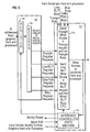
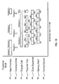
- Fig. 4A is a block diagram of the bitblt and line draw parameter calculator dataflow.
- the input parameters are received from input interface 300 and triangle interpolator 310.
- the output parameters are then calculated from the input parameters by multiplexers 510, inverters 520, carry look-ahead adders 530, divider 540 and registers 550.
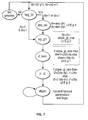
- Fig. 4B is a state flow diagram for the parameter calculator 320, with detail and emphasis on a Bresenham line sequence.
- This controller switches the multiplexers and registers depicted in Fig. 4A to complete the parameter calculation sequence.
- step slp_gtl the variable dx is compared to dy. If dy is greater than dx, then the slope of the line to be drawn creates an amgle greater than 45 degrees, so the slope_gt_one flag is set.
- step d term the slope_gt_one flag is tested to determine how the dterm variable is calculated, as shown in the comments accompanying the figure.
- the bitblt and line draw sequencer calculates frame buffer addresses, controls, colour interpolation pacing and communicates with the memory hypervisor.
- the sequencer works with data path 370 to pass address information from the sequencer and corresponding data from the data path in a coordinated manner.
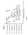
- Fig. 5 is a block diagram of the bitblt and line draw sequencer dataflow.
- Bitblt and line draw parameter calculator 320 is shown providing data to the bitblt and line draw sequencer 360.
- Sequencer 360 includes addressing control 610, arithmetic and logic units 620, 630 and 640 (also known as arithmetic units), memory request control 650 and memory interface 660.
- the arithmetic units perform the necessary calculations to draw the primitives from the data provided by the parameter calculator.
- the arithmetic units 620 and 630 handle the Y variables and arithmetic unit 640 handles the X variables.
- Addressing control 610 controls the operation of the arithmetic units and the results of their operations being passed to the memory interface.
- Fig. 6A is a more detailed block diagram of the input interface 300 shown in Fig. 2.
- An address decoder 700 includes a register 702 and a decoder 704. The decoder determines what type of request is pending and classifies the requests into different types such as overall request, triangle request, etc. There are also miscellaneous requests that are never protected. That is, an interrupt register can always be read or written.
- the request, read/write and strobe lines from the front end processor 210 and the busy signals from the rasterization processor functional blocks are all inputs to a register protection checker 710.
- the register protection checker includes an interface 712 and an interface controller state machine 714. The checker compares the type of request with the current status of the busy lines to determine if the register operation can proceed. When the operation can proceed the ready line is asserted to the front end processor and (if the register operation is a write) the write strobe line is asserted to the correct functional block.
- the register protection scheme also facilitates overlapping operations. For example, while the bitblt and line draw parameter calculator 320 is completing a line, parameters can be loaded into the triangle interpolator. This increases the performance when there is a mixture of operations to be performed. When starting an operation, the command interpreter and supervisor 340 has a separate busy signal, thereby preventing update of the start operation register until the previous operation is complete.
- the input interface allows each internal register to be protected by one or more busy signals. This allows, for example, the XY address of a line to be protected solely by the line drawer busy signal while the destination buffer selection (frame buffer, Z buffer or attribute buffer) requires all the busy signals to be inactive to prevent changing the buffer selection in the middle of an operation. Providing this differentiation allows a simple DMA controller to load any register in the rasterization processor in any order.
- the input interface prevents a register from being loaded at an improper time.
- the DMA controller can be set to copy from a display list in memory to the rasterization processor. As the rasterization processor completes operations, the next set of parameters can be loaded. Different operations can be mixed, as well as changes to overall control registers (buffer selection for example).
- fast characters By separating address and data busy signals, such as the busy from the bitblt and line draw parameter calculator 320 and the busy from the data path 370, fast characters (bitblt) can be processed with a simple DMA interface.
- the protection mechanism allows the address information (destination X, Y) of each successive character to be entered while the previous character bitblt is completed. Then the protection mechanism will feed the data path at the rate it can handle the new character image.
- Z and attribute compare there are several ways to implement Z and attribute compare in hardware.
- One is to have a single memory controller for the frame, attribute and Z buffers.
- the rasterizer front end generates address, colour and Z depth information, decides which buffer currently needs to be accessed, and sends a request to the memory controller to access the appropriate buffer. When the memory controller has finished, the rasterizer sends the next request to be processed. While Z and/or attribute compare is active, several memory requests must be sent by the rasterizer front end to write a single pixel to the destination.
- the performance of this implementation is limited primarily for three reasons. The first is that all buffer accesses must be done sequentially because there is only one memory controller. The second reason is that the process of reading the Z and/or attribute buffers, sending the data to the rasterizer front end, doing compares, deciding which buffer to access next, and sending the appropriate request to the memory controller requires many pipeline stages. This series or loop of operations must be performed for every pixel. The time required to go through this loop is almost always too long to operate at maximum memory bandwidth. The third reason is that the rasterizer front end cannot start rasterizing (i.e., generating address, colour and Z depth) the next pixel until it finishes doing the Z and/or attribute compares and writes the current pixel to the destination buffer.
- Fig. 7A is a more detailed block diagram of the memory hypervisor shown in Fig. 2.
- Parallel independent memory controllers 800, 810 and 820 are used for Z, attribute buffers, respectively. This makes it possible to execute multiple memory requests simultaneously such as reading the attribute buffer while writing the frame buffer. Even if two memory requests cannot be executed simultaneously because the buffers share data busses, it is possible to overlap the memory controllers such that the shared busses are run at maximum speed.
- a hypervisor 830 is used to initiate and control the compare operations and memory controllers. It is close (i.e., few pipeline stages) to the memory controllers, thereby allowing the compare results to be utilised quickly. This allows us to more efficiently utilise the data busses.
- Rasterizer front end requests are placed into a pipeline or buffer 840 in front of the hypervisor. This allows smoothing of the variations in performance between the rasterizer front end and the memory banks, thereby allowing each to operate at maximum speed more often. This reduces the number of instances where the memory banks are waiting for a pixel to be rasterized or the rasterizer front end is waiting for the memory accesses to complete. It also allows the hypervisor to start execution of the next memory operation while executing the current operation.
- Read and write requests are sent by the rasterizer front end to the hypervisor.
- the hypervisor When the hypervisor is ready to accept a request, it will send a grant to the rasterizer front end and latch all necessary data associated with the request.
- the rasterizer front end Upon receiving a grant, the rasterizer front end considers the request complete and begins generating the next request, even though the hypervisor has not completed the first request.
- Fig. 7B shows how the apparatus of Fig. 2 would process a series of writes to the frame buffer with Z and attribute compare being performed.
- the hypervisor immediately determines which compare options must be performed (in this example, both attribute and Z).
- On the next cycle a read request is sent to the attribute memory controller. Since this controller is inactive, it immediately sends a grant to the hypervisor and latches the address.
- the hypervisor considers the operation done upon receiving the grant and, on the next cycle, sends a read request to the Z memory controller.
- the Z and frame buffer memory share a common data bus, therefore the Z memory controller must wait until the frame buffer memory controller is done with the data bus. This wait period is determined by passing various busy signals between all the memory controllers. After the appropriate wait period, the Z memory controller sends a grant to the hypervisor. Next, a write request is sent to the Z memory controller. If the Z and/or attribute compare is false, then the Z memory controller will abort the write operation after sending the grant. Finally, a write request is sent to the frame buffer controller. Again, if the compare is false, the frame buffer controller will abort the write operation after sending the grant.
- Fig. 7C shows how the rasterizer would process a series of writes to the frame buffer with only an attribute compare being performed.
- the rasterizer front (Fig. 2) end puts a write request into the pipeline.
- the hypervisor immediately determines which compare options must be performed (in this example, only attribute compare).
- a read request is sent to the attribute memory controller. Since this controller is inactive, it immediately sends a grant to the hypervisor and latches the address.
- the hypervisor simultaneously sends a write request to the frame buffer memory controller and a read request to the attribute frame buffer (this attribute read request is for request N+1 in the pipeline, which is obtained one pipeline stage before the regular processor request). If the attribute compare is false, the frame buffer controller will abort the write operation after sending the grant.
- Fig. 8A shows how the rasterizer 220 of Fig. 2 would process a series of lines followed by a series of bitblts.
- the boxes denote when each subsystem is busy. The shading is to aid in differentiating between adjacent commands.
- For a line the sequence is as follows. The end points of the line are loaded through the input interface 300, the final value is a go signal to the command interpreter 340, the command interpreter starts the parameter calculator 320 if it is not either busy or waiting for its last set of calculated parameters to be used, the parameter calculator creates necessary values for the draw sequencer 360, and the draw sequencer makes memory requests to the memory hypervisor 380.
- the parameter calculator works on line 2 while the drawing sequencer is working on line 1.
- the memory hypervisor is kept busy. If line 3 is followed by a bitblt, the command interpreter starts the parameter calculator on the bitblt even before the drawing sequencer is finished with a line. Therefore, two different styles of commands are processed in an overlapped fashion and the memory hypervisor maintains maximum utilisation.
- Fig. 8B shows how the apparatus of Fig. 2 would process a series of triangles.
- the shading is to aid in differentiating between operations related to adjacent triangles.
- the sequence is as follows.
- the parameters of the triangle are loaded through the input interface, the final value is the go signal to the command interpreter, the command interpreter starts triangle interpolator 220 if it is not busy, the triangle interpolator feeds a series of lines (or spans) to the parameter calculator if it is free, the parameter calculator creates the necessary values for the draw sequencer and the draw sequencer makes memory requests to the memory hypervisor.
- the third triangle cannot be loaded until the first is completely interpolated. Once the first span of a triangle is started, the memory hypervisor is kept busy.
- the triangle interpolator has internal storage for two sets of parameters so that there is not an unused stretch of time after one triangle is done while the input interface is busy receiving new parameters for the next
- Fig. 8C shows how the apparatus of Fig. 2 would process a series of external bitblts which require format conversion of the input data (such as a character expansion).
- the shading is to aid in differentiating between operations related to adjacent bitblts.
- the sequence is as follows. The parameters of the bitblt are loaded through the input interface, the final value is the go signal to the command interpreter, the command interpreter starts the parameter calculator if it is free, the parameter calculator creates the necessary values for the draw sequencer and the format converter 330, the bitblt data can now begin to come via the input interface which passes it to the format converter, and the draw sequencer makes memory requests to the memory hypervisor once the data path 370 has the data from the format converter.
- the format converter has an internal FIFO so that it can get ahead of the draw sequencer, thereby allowing the input interface to finish early. Then the parameters for bitblt 2 can be loaded restarting the whole sequence. If the format converter FIFO is large enough and the input interface loads faster than the memory hypervisor can write the pixels, then the memory can be kept utilised. Certainly for characters this is true since for each bit of input data a pixel of output data is generated which is typically 3 bytes (24-bit pixels).
- Overlapping operations are supported by having interlocks among the various state machines which allow subsequent operations to begin before the current operation is complete whenever possible.
- the input interface allows new values to be loaded in registers that are either currently not used or no longer required to be stable.
- the command interpreter determines which subsystems are involved in the previous command and allows a new command to proceed if the first active block for the new command is not busy processing the previous command. For example, as shown in Fig. 8D), if the new command is a triangle and the previous command was a line (a bitblt would similar), then the command interpreter would pass the triangle interpolator the start triangle signal.
- the triangle interpolator would then proceed to create the first horizontal span of the triangle, but parameter calculation for that span would be held off until the bitblt and line draw parameter calculator was free. If the line is long enough (or the bitblt large enough), then the input interface loads the triangle before the memory hypervisor completes the previous operation. The first line of the triangle can also be calculated while the previous line is being drawn, keeping the memory utilised. However, when a bitblt follows a triangle, the input interface prevents the bitblt parameters from being loaded until after the last line of the triangle is completed. This would leave a gap in the memory utilisation depending on the length of the last line. In Fig. 8D, a small gap is shown, but most lines are long enough so that no gap would exist.
Landscapes
- Engineering & Computer Science (AREA)
- Computer Graphics (AREA)
- Physics & Mathematics (AREA)
- General Physics & Mathematics (AREA)
- Theoretical Computer Science (AREA)
- Image Generation (AREA)
- Controls And Circuits For Display Device (AREA)
Applications Claiming Priority (2)
| Application Number | Priority Date | Filing Date | Title |
|---|---|---|---|
| US07/614,357 US5420972A (en) | 1990-11-15 | 1990-11-15 | Method and apparatus for rendering lines |
| US614357 | 1990-11-15 |
Publications (2)
| Publication Number | Publication Date |
|---|---|
| EP0486195A2 true EP0486195A2 (de) | 1992-05-20 |
| EP0486195A3 EP0486195A3 (en) | 1993-11-10 |
Family
ID=24460909
Family Applications (1)
| Application Number | Title | Priority Date | Filing Date |
|---|---|---|---|
| EP19910310161 Withdrawn EP0486195A3 (en) | 1990-11-15 | 1991-11-04 | Computer graphics system |
Country Status (4)
| Country | Link |
|---|---|
| US (1) | US5420972A (de) |
| EP (1) | EP0486195A3 (de) |
| JP (1) | JPH0714029A (de) |
| CA (1) | CA2055783A1 (de) |
Cited By (2)
| Publication number | Priority date | Publication date | Assignee | Title |
|---|---|---|---|---|
| AU699532B2 (en) * | 1994-09-16 | 1998-12-03 | Canon Kabushiki Kaisha | Object based rendering system |
| AU727990B2 (en) * | 1997-04-30 | 2001-01-04 | Canon Kabushiki Kaisha | Graphics processing system |
Families Citing this family (8)
| Publication number | Priority date | Publication date | Assignee | Title |
|---|---|---|---|---|
| US5634093A (en) * | 1991-01-30 | 1997-05-27 | Kabushiki Kaisha Toshiba | Method and CAD system for designing wiring patterns using predetermined rules |
| CA2127370C (en) * | 1992-01-21 | 1999-02-23 | Thomas Michael Albers | Video graphics controller with improved calculation capabilities |
| US5613053A (en) | 1992-01-21 | 1997-03-18 | Compaq Computer Corporation | Video graphics controller with automatic starting for line draws |
| US5621866A (en) * | 1992-07-24 | 1997-04-15 | Fujitsu Limited | Image processing apparatus having improved frame buffer with Z buffer and SAM port |
| US5666520A (en) * | 1993-03-29 | 1997-09-09 | Hitachi, Ltd. | Graphics display system including graphics processor having a register storing a series of vertex data relating to a polygonal line |
| US5625768A (en) * | 1994-05-23 | 1997-04-29 | Cirrus Logic, Inc. | Method and apparatus for correcting errors in pixel characteristics when interpolating polygons into a pixel grid |
| US6445386B1 (en) * | 1999-01-15 | 2002-09-03 | Intel Corporation | Method and apparatus for stretch blitting using a 3D pipeline |
| US6891541B1 (en) * | 1999-03-31 | 2005-05-10 | Texas Instruments Incorporated | Graphing calculator with manual line drawing |
Family Cites Families (22)
| Publication number | Priority date | Publication date | Assignee | Title |
|---|---|---|---|---|
| JPS57119390A (en) * | 1981-01-16 | 1982-07-24 | Tokyo Shibaura Electric Co | Shading method |
| JPS5971093A (ja) * | 1982-10-18 | 1984-04-21 | 株式会社日立製作所 | 塗潰し図形発生装置 |
| US4609917A (en) * | 1983-01-17 | 1986-09-02 | Lexidata Corporation | Three-dimensional display system |
| US4586038A (en) * | 1983-12-12 | 1986-04-29 | General Electric Company | True-perspective texture/shading processor |
| US4725831A (en) * | 1984-04-27 | 1988-02-16 | Xtar Corporation | High-speed video graphics system and method for generating solid polygons on a raster display |
| US4648049A (en) * | 1984-05-07 | 1987-03-03 | Advanced Micro Devices, Inc. | Rapid graphics bit mapping circuit and method |
| US4677573A (en) * | 1984-05-15 | 1987-06-30 | International Business Machines Corporation | Hardware generation of styled vectors in a graphics system |
| US4697178A (en) * | 1984-06-29 | 1987-09-29 | Megatek Corporation | Computer graphics system for real-time calculation and display of the perspective view of three-dimensional scenes |
| US4658247A (en) * | 1984-07-30 | 1987-04-14 | Cornell Research Foundation, Inc. | Pipelined, line buffered real-time color graphics display system |
| US4679041A (en) * | 1985-06-13 | 1987-07-07 | Sun Microsystems, Inc. | High speed Z-buffer with dynamic random access memory |
| US4758965A (en) * | 1985-10-09 | 1988-07-19 | International Business Machines Corporation | Polygon fill processor |
| US4805116A (en) * | 1986-04-23 | 1989-02-14 | International Business Machines Corporation | Interpolated display characteristic value generator |
| JPH0812705B2 (ja) * | 1986-09-29 | 1996-02-07 | 株式会社東芝 | 画像処理装置 |
| JPS6394378A (ja) * | 1986-10-08 | 1988-04-25 | Seiko Instr & Electronics Ltd | 直線発生回路 |
| US5001651A (en) * | 1986-11-10 | 1991-03-19 | Auto-Trol Technology Corporation | Method and apparatus for interpolating groups of pixels on a scan line |
| US5113494A (en) * | 1987-02-27 | 1992-05-12 | Eastman Kodak Company | High speed raster image processor particularly suited for use in an image management system |
| US5010515A (en) * | 1987-07-28 | 1991-04-23 | Raster Technologies, Inc. | Parallel graphics processor with workload distributing and dependency mechanisms and method for distributing workload |
| DE3854707T2 (de) * | 1987-07-30 | 1996-07-25 | Tektronix Inc | Verfahren und Gerät zur inkrementalen Berechnung einer linearen Funktion. |
| US5185599A (en) * | 1987-10-26 | 1993-02-09 | Tektronix, Inc. | Local display bus architecture and communications method for Raster display |
| JP2618951B2 (ja) * | 1988-02-16 | 1997-06-11 | 株式会社東芝 | 三次元図形処理装置 |
| US4958303A (en) * | 1988-05-12 | 1990-09-18 | Digital Equipment Corporation | Apparatus for exchanging pixel data among pixel processors |
| US4951229A (en) * | 1988-07-22 | 1990-08-21 | International Business Machines Corporation | Apparatus and method for managing multiple images in a graphic display system |
-
1990
- 1990-11-15 US US07/614,357 patent/US5420972A/en not_active Expired - Fee Related
-
1991
- 1991-08-20 JP JP3231085A patent/JPH0714029A/ja active Pending
- 1991-10-22 CA CA002055783A patent/CA2055783A1/en not_active Abandoned
- 1991-11-04 EP EP19910310161 patent/EP0486195A3/en not_active Withdrawn
Cited By (2)
| Publication number | Priority date | Publication date | Assignee | Title |
|---|---|---|---|---|
| AU699532B2 (en) * | 1994-09-16 | 1998-12-03 | Canon Kabushiki Kaisha | Object based rendering system |
| AU727990B2 (en) * | 1997-04-30 | 2001-01-04 | Canon Kabushiki Kaisha | Graphics processing system |
Also Published As
| Publication number | Publication date |
|---|---|
| US5420972A (en) | 1995-05-30 |
| CA2055783A1 (en) | 1992-05-16 |
| EP0486195A3 (en) | 1993-11-10 |
| JPH0714029A (ja) | 1995-01-17 |
Similar Documents
| Publication | Publication Date | Title |
|---|---|---|
| US5457775A (en) | High performance triangle interpolator | |
| US5452412A (en) | High performance rasterization engine | |
| US4725831A (en) | High-speed video graphics system and method for generating solid polygons on a raster display | |
| US5097411A (en) | Graphics workstation for creating graphics data structure which are stored retrieved and displayed by a graphics subsystem for competing programs | |
| US4928247A (en) | Method and apparatus for the continuous and asynchronous traversal and processing of graphics data structures | |
| KR960003041B1 (ko) | 그래픽 시스템용의 확장 가능한 다영상 버퍼 | |
| US5185599A (en) | Local display bus architecture and communications method for Raster display | |
| US5790134A (en) | Hardware architecture for image generation and manipulation | |
| US5251322A (en) | Method of operating a computer graphics system including asynchronously traversing its nodes | |
| US20080211805A1 (en) | Method and System for Minimizing an Amount of Data Needed to Test Data Against Subarea Boundaries in Spatially Composited Digital Video | |
| US5155822A (en) | High performance graphics workstation | |
| US5877769A (en) | Image processing apparatus and method | |
| US7525547B1 (en) | Programming multiple chips from a command buffer to process multiple images | |
| GB2245129A (en) | Local display bus architecture and communications method for raster display | |
| JPH1097635A (ja) | ディスプレイリストを生成する方法、ディスプレイリストを受け取りグラフィックスプロセッサに格納する方法、プリミティブをレンダリングする方法およびディスプレイリストを用いてプリミティブをレンダリングするシステム | |
| US5420972A (en) | Method and apparatus for rendering lines | |
| US6275241B1 (en) | High speed image drawing apparatus for displaying three dimensional images | |
| EP0644509B1 (de) | Verfahren und Gerät zum Füllen von Polygonen | |
| US5339394A (en) | I/O register protection circuit | |
| US5511154A (en) | Method and apparatus for managing concurrent access to multiple memories | |
| JPH08249502A (ja) | 補助バッファ情報を用いる改良型グラフィクス・ピッキング方法及び装置 | |
| JPH09231385A (ja) | オブジェクトのラスタ化方法及び装置 | |
| Haaker et al. | A distributed frame buffer within a window-oriented high performance graphics system | |
| JP2836617B2 (ja) | レンダリングプロセッサ | |
| Joseph | A Distributed Frame Buffer within a Window-Oriented High Performance Graphics System |
Legal Events
| Date | Code | Title | Description |
|---|---|---|---|
| PUAI | Public reference made under article 153(3) epc to a published international application that has entered the european phase |
Free format text: ORIGINAL CODE: 0009012 |
|
| AK | Designated contracting states |
Kind code of ref document: A2 Designated state(s): DE FR GB IT |
|
| PUAL | Search report despatched |
Free format text: ORIGINAL CODE: 0009013 |
|
| AK | Designated contracting states |
Kind code of ref document: A3 Designated state(s): DE FR GB IT |
|
| STAA | Information on the status of an ep patent application or granted ep patent |
Free format text: STATUS: THE APPLICATION IS DEEMED TO BE WITHDRAWN |
|
| 18D | Application deemed to be withdrawn |
Effective date: 19940531 |