EP0486322A2 - Appareil pour le réglage automatique d'un filtre - Google Patents
Appareil pour le réglage automatique d'un filtre Download PDFInfo
- Publication number
- EP0486322A2 EP0486322A2 EP91310571A EP91310571A EP0486322A2 EP 0486322 A2 EP0486322 A2 EP 0486322A2 EP 91310571 A EP91310571 A EP 91310571A EP 91310571 A EP91310571 A EP 91310571A EP 0486322 A2 EP0486322 A2 EP 0486322A2
- Authority
- EP
- European Patent Office
- Prior art keywords
- filter
- adjusting
- signal
- channel
- automatic
- Prior art date
- Legal status (The legal status is an assumption and is not a legal conclusion. Google has not performed a legal analysis and makes no representation as to the accuracy of the status listed.)
- Withdrawn
Links
- 238000000034 method Methods 0.000 claims description 5
- 230000004044 response Effects 0.000 claims description 2
- 230000005236 sound signal Effects 0.000 description 21
- 239000003990 capacitor Substances 0.000 description 16
- 238000010586 diagram Methods 0.000 description 9
- 230000010354 integration Effects 0.000 description 7
- 230000002238 attenuated effect Effects 0.000 description 4
- 238000004519 manufacturing process Methods 0.000 description 4
- 230000008859 change Effects 0.000 description 3
- 238000001514 detection method Methods 0.000 description 3
- 230000008901 benefit Effects 0.000 description 2
- 238000010276 construction Methods 0.000 description 2
- 230000006870 function Effects 0.000 description 2
- 230000004048 modification Effects 0.000 description 2
- 238000012986 modification Methods 0.000 description 2
- 239000004065 semiconductor Substances 0.000 description 2
- 238000000926 separation method Methods 0.000 description 2
- 230000003321 amplification Effects 0.000 description 1
- 230000000295 complement effect Effects 0.000 description 1
- 230000007547 defect Effects 0.000 description 1
- 239000000463 material Substances 0.000 description 1
- 238000003199 nucleic acid amplification method Methods 0.000 description 1
- 230000009467 reduction Effects 0.000 description 1
- 238000001228 spectrum Methods 0.000 description 1
Images


Classifications
-
- H—ELECTRICITY
- H03—ELECTRONIC CIRCUITRY
- H03H—IMPEDANCE NETWORKS, e.g. RESONANT CIRCUITS; RESONATORS
- H03H7/00—Multiple-port networks comprising only passive electrical elements as network components
-
- H—ELECTRICITY
- H04—ELECTRIC COMMUNICATION TECHNIQUE
- H04N—PICTORIAL COMMUNICATION, e.g. TELEVISION
- H04N5/00—Details of television systems
- H04N5/76—Television signal recording
- H04N5/78—Television signal recording using magnetic recording
- H04N5/782—Television signal recording using magnetic recording on tape
- H04N5/78213—Television signal recording using magnetic recording on tape involving recording in different depths of the magnetic tape
-
- G—PHYSICS
- G11—INFORMATION STORAGE
- G11B—INFORMATION STORAGE BASED ON RELATIVE MOVEMENT BETWEEN RECORD CARRIER AND TRANSDUCER
- G11B20/00—Signal processing not specific to the method of recording or reproducing; Circuits therefor
- G11B20/02—Analogue recording or reproducing
- G11B20/06—Angle-modulation recording or reproducing
-
- H—ELECTRICITY
- H04—ELECTRIC COMMUNICATION TECHNIQUE
- H04N—PICTORIAL COMMUNICATION, e.g. TELEVISION
- H04N9/00—Details of colour television systems
- H04N9/79—Processing of colour television signals in connection with recording
- H04N9/80—Transformation of the television signal for recording, e.g. modulation, frequency changing; Inverse transformation for playback
- H04N9/802—Transformation of the television signal for recording, e.g. modulation, frequency changing; Inverse transformation for playback involving processing of the sound signal
Definitions
- the present invention relates generally to an automatic filter adjusting apparatus, and, more particularly, to an automatic filter adjusting apparatus suitable for band pass filters of audio systems in VTRs.
- VTR video tape recorders
- Hi-Fi VTRs Hi-Fi VTRs
- a so-called deep layer recording technique has been recently developed.
- two channel audio signals are modulated with different frequencies and then multiplexed with each other.
- the multiplexed FM (frequency modulation) audio signal is recorded on an audio track of a video tape over a relatively thick layer thereof.
- the multiplexed FM audio signal is reproduced from the audio track of the video tape by a reproducing head. Then two channel audio signals are separated from the multiplexed FM audio signal, by using band pass filters (BPFs) with different frequency bands.
- BPFs band pass filters
- FIGURE 1 Shown in FIGURE 1 is a block diagram illustrating an audio system of conventional Hi-Fi VTRs.
- Two channel audio signals i.e., left (L) channel and right (R) channel audio signals, are applied to L channel and R channel de-emphasis encoders 2, of a recording system.
- These encoders 2, 3 constitute a well-known noise reduction system in co-operation with emphasis decoders 15, 16 in a reproduction system, which will be referred to later.
- the L channel and R channel audio signals have their amplitudes expanded at a prescribed frequency level to remove noise components.
- the compressed amplitude audio signals are applied to FM modulators 4, 5, respectively.
- the L channel, R channel FM signals are then combined together in a mixer 6.
- the combined signal is supplied to a recording head 8 after amplification by an amplifier 7.
- the signal is then recorded on an audio track of video tapes (not shown).
- the recorded signal is reproduced through a reproducing head 9.
- the reproduced signal has the configuration of the multiplexed FM audio signal.
- the reproduced signal from the reproducing head 9 is then applied to both an L channel BPF 11 and an R channel BPF 12 through an amplifier 10.
- These BPFs 11, 12 have different frequency bands which correspond to the frequencies of the FM modulators 4, 5, respectively.
- the L channel FM audio signal is extracted from the L channel BPF 11, while the R channel FM audio signal is extracted from the R channel BPF 12.
- These FM audio signals are applied to FM demodulators 13, 14 so that audible band L channel and R channel audio signals are demodulated therefrom.
- These audible band L channel and R channel audio signals are applied to the above-mentioned emphasis decoders 15, 16.
- the L channel and Rchannel audio signals have their amplitudes compressed at a prescribed level which is complementary to those of the de-emphasis encoders 2, 3.
- the original L channel and R channel audio signals are obtained through output terminals.
- these passbands are isolated by a narrow band of only 100 KHz so that the channel separation performance can be remarkably deteriorated unless the centers of the BPFs are precisely realized.
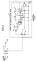
- FIGURE 2 shows an R channel filter 27 in the form of a BPF and an adjusting circuit for the BPF 27.
- an FM audio signal is applied from an input terminal 27a to the BPF 27.
- An output of the BPF 27 is led to an output terminal 27b.
- the time constant of the BPF 27 is adjusted by an automatic time constant adjusting circuit 18 as follows.
- the automatic time constant adjusting circuit 18 is constituted by an integration circuit 17, a switch 21, a peak hold circuit 20, a comparator 19 and a reference voltage source 25.
- the integration circuit 17 includes a variable transconductor 24 with its input terminals supplied with a reference voltage Vref from a reference voltage source 25, a capacitor 22 coupled to the output terminal of the transconductor 24 and a variable current source 23 for biasing the transconductor 24.
- the switch 21 is connected in parallel to the capacitor 22 for periodically short-circuiting the capacitor 22 under the control of a clock signal. Thus a triangular pulse signal as shown in the drawing is generated on the terminal of the capacitor 22.
- the triangular pulse signal is applied to the peak hold circuit 20, wherein the peak voltage of the triangular pulse signal is held.
- the peak voltage is supplied to an input terminal of the comparator 19.
- the comparator 19 compares the peak voltage with the reference voltage Vref. Then a difference voltage obtained on the output terminal of the comparator 19 is supplied to a capacitor 26 having a large capacitance for charging it.
- the terminal voltage of the capacitor 26 is applied to both the BPF 27 and the variable current source 23.
- the voltage applied to the current source 23 causes the control current of the current source 23 to vary.
- the integration circuit 17, the switch 21, the comparator 19, the capacitor 26 and the current source 23 constitute a control loop for automatically adjusting the time constant of the transconductor 24.
- the transconductance gm of the transconductor 24 is varied by a difference between the peak level of the triangular pulse signal and the reference voltage Vref.
- the variation of the transconductance gm causes the amount of a current applied to the capacitor 23 from the transconductor 24 to vary.
- the slope of the triangular pulse signal varies in response to the amount of the current.
- the peak level is higher than the reference voltage Vref
- the slope becomes lower.
- the peak level of the triangular pulse signal comes to agree with the reference voltage Vref.
- T denotes a pulse period of the clock signal
- Co denotes the capacitance of the capacitor 22.
- the above equation (1) shows that the right side, which represents the time constant of the integration circuit 17, is defined by only the pulse period T. In other words, the time constant of the integration circuit 17 is precisely adjusted if the clock signal has a stable frequency.
- the automatically adjusted BPF 27 also consists of a variable transconductor of the same type as the transconductor 24 in the automatic time constant adjusting circuit 18. It is also assumed that an adjusting signal Va applied to the BPF 27 from the automatic time constant adjusting circuit 18 is the same as the signal applied to the current source 23 of the integration circuit 17. Under these conditions, the transfer function H(S) of the BPF 27 subjected to the adjustment, which is the same as that of the transconductor 24, is expressed by the following equation.
- the time constant of the BPF 27 is accurately decided by the automatic time constant adjusting circuit 18.
- the frequency characteristic of the BPF 27 is decided relying only on the accuracy of the automatic time constant adjusting circuit 18, i.e., the error of the time constant Co/gm of the integration circuit 17.
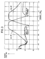
- such a BPF has a sharp attenuation characteristic as shown in FIGURE 3. If the passing band center frequency of such a filter deviates largely from the actual FM signal frequency, not only the channel separation is deteriorated, but, when FM signals having wide spectra in case of large amplitude or when high modulation frequencies are applied, distortion after demodulation is also increased.
- BPFs It is therefore indispensable for BPFs to have a means to perform the manual adjustment from the outside and furthermore, the adjustment is necessary for every channel.
- the conventional automatic filter adjusting system requires an accurate clock and a capacitor having a large capacitance but it has such defects that temperature drift and voltage drop drift tend to occur and their compensation is difficult and furthermore, circuit scale can become large.
- the present invention therefore seeks to provide an automatic filter adjusting apparatus which is able to automatically adjust filters to desired frequency characteristics.
- the present invention also seeks to provide an automatic filter adjusting apparatus which is able to be made in a single chip IC.
- An automatic filter adjusting apparatus includes a reference signal provider for providing an FM signal to the filter, an adjusting signal generator for providing an adjusting signal to the filter, a comparator for comparing the output of the filter to a reference level and a controller responsive to the comparator for controlling the adjusting signal generator.
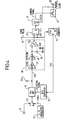
- FIGURE 4 shows an adjusting circuit for a BPF such as an R channel BPF 34 (corresponding to the BPF 12 of FIGURE 1) of an audio system for "Hi-Fi VTRs".
- a BPF such as an R channel BPF 34 (corresponding to the BPF 12 of FIGURE 1) of an audio system for "Hi-Fi VTRs".
- a R channel audio signal is applied to the BPF 34 through a switch 33.
- the switch 33 is adapted for selectively applying either the R.channel audio signal from an input terminal 31 or a non-signal carrier from a modulator 32 of the other channel.
- the output from the output terminal 34a of the BPF 34 is applied to a demodulator (not shown) of a next stage.
- the automatic adjusting circuit adjusts the frequency characteristics of the filters, e.g., the R.channel BPF 34 as described above.
- the BPF 34 incorporates, for instance, a variable transconductor and is capable of setting up frequency characteristics by controlling current from the current source of the variable transconductor.
- the adjusting signal for the frequency characteristic adjustment is given from a digital/analog converter 35. During the period of the normal operation of a VTR, that is, when the VTR is performing the reproduction operation, the adjusting signal is held at a set value.
- the output terminal of the BPF 34 is connected to the input terminal of a level detector 36.
- the level detector 36 consists of an amplifier 37 to which an input terminal 36a of the level detector 36 is connected, a DC converter 38 which detects the output from the amplifier 37, a capacitor 39 which smooths the output of the DC converter 38, and a comparator 40 which compares the output from the capacitor 39 with a reference voltage Vref.
- the comparator 40 outputs a coincidence pulse when the terminal voltage of the capacitor 39 agrees with the reference voltage Vref and sets a flip-flop circuit 41.
- the flip-flop circuit 41 When the flip-flop circuit 41 is set, its Q output becomes high level and is latched by a latch circuit 42 to turn off a switch 43.
- the switch 43 When the switch 43 is turned off, a clock being supplied from a terminal 45 to a counter44 is stopped and a count value of the counter 44 is held at its current state.
- the output from the counter 44 is applied to the D/A converter 35.
- the flip-flop circuit 41 is first reset by the start pulse from the terminal 46 and the counter 44 is cleared. Then, the switch 43 is turned ON K clocks later. As a result, the output from the D/A converter 35, that is, the adjusting signal, becomes large with the increase of a count value of the counter 44. Then, the frequency characteristic of the BPF 34 is shifted in the direction of higher frequency on the frequency axis according to the change of the adjusting signal.
- the center frequency of another channel being supplied to the BPF 34 from the modulator 32 is gradually attenuated. Then, when a sufficient attenuation characteristic is obtained (the center frequency band of the channel), the supply of clock signals is stopped, the counter stops operating, and the adjusting signal at that time is held.
- FIGURE 3 shows the ideal relation between the center frequency of the adjusted channel and another channel and the frequency characteristics of the BPF of each channel.
- the band-pass characteristic indicates FM signal frequency bands of, for instance, the L and R channel of the audio system of Hi-Fi VTRs.
- the center frequencies of FM signals of L channel and R channel are specified as follows:
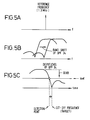
- the center frequency (1.3 MHz) (FIGURE 5A) which becomes the reference frequency for the L channel is applied to the BPF 34 by the switch 33.
- the band pass characteristic of the BPF 34 is shifted gradually from the low frequency region to the high frequency region as shown in FIGURE 5B.
- the center frequency 1.3 MHz passes while getting a sufficient gain, but it is gradually attenuated and finally, the output characteristic of the BPF 34 becomes that shown in FIGURE 5C.
- the characteristic corresponds to the input to the comparator 40 of the level detector 36. If the reference voltage Vref is set at -30 dB as shown in FIGURE 5C, after passing the K clocks period, the supply of clocks is stopped, and it becomes possible to set the frequency characteristics at the level (the ideal frequency characteristics of the R channel shown in FIGURE 3) where another channel's center frequency can be fully attenuated. Thereafter, the value of the counter 44 at that time is held and the characteristics after the adjustment are maintained.
- the filter adjustment is made for each channel at the time of the system start-up, when the system is paused, or at the time of the recording.
- a counter similar to the counter 44 or a latch circuit is provided for each channel.
- the coincidence pulse is obtained from the comparator 40 at a level of -30 dB and the supply of clock signals is stopped at the eighth clock after detecting the coincidence pulse.
- The is because it has been so set that the output amplitude becomes minimum when the output from the BPF 37 is attenuated at 1.3 MHz.
- the comparison level by the reference voltage Vref should be as deep as possible because more precise adjustment becomes possible.
- the comparison level has been set several clock signals on the side of the extremity of attenuation to assure positive detection with a lower number of bits, as described above.
- the comparison level can be set relatively shallow and the location of the extremity of attenuation can be precisely estimated without detection error and free from influence of characteristic fluctuation.
- the bit size of the counter 44 is 7 bits
- the clock signal is 100 KHz
- fluctuation of the passive elements such as resistors and capacitors in IC chips is ⁇ 20%
- the range of fluctuation of the center frequency of the BPF before adjusting- is 1.09 to 2.45 MHz
- the adjusting step is 10.6 KHz with the same adjusting range as the fluctuation range
- fluctuation of the center frequency of the BPF after adjustment will become 1.695 to 1.705 MHz.
- the fluctuation is about 1/17 of conventional filter fluctuation and sufficient accuracy is obtained. In principle, it is possible to further promote accuracy when the number of bits of the counter is further increased. Further, a time required for the adjustment is as short as maximum 1.28 sec. and there is no restriction by the adjusting time.
- the adjustment can be updated for drifting factors of the filter characteristics such as temperature, supply voltage change and the like.
- the embodiment has such merit as external elements and excess IC pins are not required an accuracy of D/A converter is not needed.
- a high accuracy signal is often available as the reference signal in the system without providing a special source for generating a reference signal and as the signal is effectively usable, a system of efficient price utilization can be constructed.
- an external input signal or a system clock signal can be used as the reference signal.
- an up-counter is used for the counter 44 to shift the BPF characteristic to a higher frequency region.
- a non-signal carrier with the center frequency of 1.7 MHz and a cut-off frequency of 1. 3 MHz, which is used for a R channel recording/repro- ducing is utilized for the adjustment.
- a down-counter is used for the counter 44 to shift the BPF characteristic to a lower frequency region.
- FIGURE 6 shows another embodiment of the present invention.
- the embodiment shown in FIGURE 4 is an example of the on chip adjustment performed every time.
- the adjustment is made in the VTR manufacturing process and adjustment data is stored in a ROM.
- the principle of adjustment is the same as the preceding embodiment.
- FIGURE 6 is effective for a system where the control IC is connected by the internal bus in a system with the host CPU of VTR set.
- the same symbols as in FIGURE 4 have been assigned to the circuits with the same purpose as those shown in FIGURE 4.
- the filtercharac- teristics in the normal operation are set by giving data stored in the memory 50 to the D/A converter 35 as the control quantity.
- control data for setting up frequency characteristics has been pre-stored as the optimum data in the memory 50, and is read under the control of the CPU 51 in the VTR, and given to the D/A converter 35.
- the data is given, for instance, when the power source is turned ON.
- the flip-flop circuit 41 is reset by the CPU 61 that is used as the adjusting unit in the manufacturing process. Further, the center frequency of another channel from the modulator 32 in the VTR is applied to the BPF 34 via the switch 33. The output from the BPF 33 is applied to the level detector 36. When the coincidence pulse is obtained from the comparator40 of the circuit 36, the flip-flop circuit 41 is set and its output is read by the CPU.
- the CPU 51 stores the optimum control data in the memory 50 via the input/output circuit 53.
- optimum control data for BPF can be stored in a memory utilizing the CPU incorporated in a VTR. It is therefore not necessary to construct the adjusting circuit on a chip as described in the above embodiment and the circuit scale can be simplified.
- the present invention can provide an extremely preferable automatic filter adjusting apparatus.
Landscapes
- Engineering & Computer Science (AREA)
- Signal Processing (AREA)
- Multimedia (AREA)
- Networks Using Active Elements (AREA)
- Filters And Equalizers (AREA)
Applications Claiming Priority (2)
| Application Number | Priority Date | Filing Date | Title |
|---|---|---|---|
| JP307305/90 | 1990-11-15 | ||
| JP2307305A JP2829123B2 (ja) | 1990-11-15 | 1990-11-15 | 自動調整icフィルタ回路 |
Publications (2)
| Publication Number | Publication Date |
|---|---|
| EP0486322A2 true EP0486322A2 (fr) | 1992-05-20 |
| EP0486322A3 EP0486322A3 (en) | 1992-09-02 |
Family
ID=17967551
Family Applications (1)
| Application Number | Title | Priority Date | Filing Date |
|---|---|---|---|
| EP19910310571 Withdrawn EP0486322A3 (en) | 1990-11-15 | 1991-11-15 | Automatic filter adjusting apparatus |
Country Status (4)
| Country | Link |
|---|---|
| US (1) | US5227743A (fr) |
| EP (1) | EP0486322A3 (fr) |
| JP (1) | JP2829123B2 (fr) |
| KR (1) | KR960006636B1 (fr) |
Families Citing this family (12)
| Publication number | Priority date | Publication date | Assignee | Title |
|---|---|---|---|---|
| US5416438A (en) * | 1992-03-18 | 1995-05-16 | Nec Corporation | Active filter circuit suited to integration on IC chip |
| KR100312623B1 (ko) * | 1993-02-26 | 2001-12-28 | 이데이 노부유끼 | 액티브필터회로장치 |
| JP2822891B2 (ja) * | 1994-08-31 | 1998-11-11 | 日本電気株式会社 | 自動調整フィルタ回路 |
| US5945889A (en) * | 1997-08-13 | 1999-08-31 | Texas Instruments Incorporated | Method and apparatus for tuning high Q bandpass filters using pulse excitation |
| FI107090B (fi) * | 1999-04-19 | 2001-05-31 | Nokia Mobile Phones Ltd | Menetelmä ja järjestely resonaattorin virittämiseksi |
| US6307443B1 (en) * | 1999-09-24 | 2001-10-23 | Agere Systems Guardian Corp. | Bandpass filters with automatic tuning adjustment |
| US6810124B1 (en) | 1999-10-08 | 2004-10-26 | The Boeing Company | Adaptive resonance canceller apparatus |
| US7082293B1 (en) * | 1999-10-21 | 2006-07-25 | Broadcom Corporation | Adaptive radio transceiver with CMOS offset PLL |
| JP3449970B2 (ja) * | 2000-07-21 | 2003-09-22 | 松下電器産業株式会社 | 相互コンダクタンス−容量フィルタシステム |
| US7761067B1 (en) * | 2003-05-15 | 2010-07-20 | Marvell International Ltd. | Iterative filter circuit calibration |
| JP2009033323A (ja) * | 2007-07-25 | 2009-02-12 | Fujitsu Microelectronics Ltd | カットオフ周波数調整方法、GmCフィルタ回路及び半導体装置 |
| US9319029B1 (en) | 2015-06-19 | 2016-04-19 | Clover Network, Inc. | System and method for automatic filter tuning |
Family Cites Families (7)
| Publication number | Priority date | Publication date | Assignee | Title |
|---|---|---|---|---|
| JPS54110761A (en) * | 1978-02-17 | 1979-08-30 | Matsushita Electric Ind Co Ltd | Automatic frequency following type band pass filter |
| IT1156199B (it) * | 1978-04-18 | 1987-01-28 | Selenia Ind Elettroniche | Perfezionamento nei circuiti si sintonia automatica per filtri controllati in tensione mediante controllo di fase digitale |
| JPS59157806A (ja) * | 1983-02-28 | 1984-09-07 | Nec Home Electronics Ltd | ビデオテ−プレコ−ダ |
| DE3546599C2 (fr) * | 1984-11-20 | 1993-06-03 | Olympus Optical Co., Ltd., Tokio/Tokyo, Jp | |
| JPS61144912A (ja) * | 1984-12-19 | 1986-07-02 | Hitachi Ltd | フイルタ集積回路 |
| JPH07120923B2 (ja) * | 1986-12-27 | 1995-12-20 | ソニー株式会社 | フイルタ調整装置 |
| JP2812708B2 (ja) * | 1988-05-18 | 1998-10-22 | 日本カーバイド工業株式会社 | シアナミドの製法 |
-
1990
- 1990-11-15 JP JP2307305A patent/JP2829123B2/ja not_active Expired - Lifetime
-
1991
- 1991-11-13 KR KR1019910020134A patent/KR960006636B1/ko not_active Expired - Fee Related
- 1991-11-14 US US07/791,387 patent/US5227743A/en not_active Expired - Fee Related
- 1991-11-15 EP EP19910310571 patent/EP0486322A3/en not_active Withdrawn
Also Published As
| Publication number | Publication date |
|---|---|
| KR920011058A (ko) | 1992-06-27 |
| US5227743A (en) | 1993-07-13 |
| JP2829123B2 (ja) | 1998-11-25 |
| KR960006636B1 (ko) | 1996-05-22 |
| EP0486322A3 (en) | 1992-09-02 |
| JPH04180406A (ja) | 1992-06-26 |
Similar Documents
| Publication | Publication Date | Title |
|---|---|---|
| US5227743A (en) | Automatic filter adjusting apparatus | |
| JPS6025801B2 (ja) | 録音バイアス電流自動調整装置 | |
| US3854098A (en) | Multichannel disc demodulation circuit | |
| US4539602A (en) | Time axis correction device for multiplex information-carrying signal obtained from recording medium | |
| US5260843A (en) | Magnetic recording and reproducing apparatus with individual correction of amplitude variations of recording currents supplied to plural rotary magnetic heads | |
| JPS6087469A (ja) | ドロップアウト補償装置 | |
| KR100466900B1 (ko) | 자기-테이프기록의경우트래킹제어를위한파일럿-톤검출회로및방법 | |
| US5982574A (en) | Automatic tracking frequency servo demodulation technique for DVCR applications | |
| US5619340A (en) | Video reproducing apparatus having filter circuit of automatic frequency adjustment type | |
| US6259315B1 (en) | FM demodulator being tuned to reference frequency by auxiliary detector | |
| KR100230163B1 (ko) | 집적 회로 및 집적 회로의 가변 필터 조정 방법 | |
| US3997915A (en) | Frequency modulating and demodulating method and apparatus | |
| KR890005007B1 (ko) | 자기 기록 재생 장치 | |
| KR890002048Y1 (ko) | 녹음기의 특정 주파수 선택회로 | |
| JP2713629B2 (ja) | 磁気記録再生装置 | |
| JPS593711A (ja) | 雑音除去装置 | |
| JPH0442750B2 (fr) | ||
| JPS6253513A (ja) | リミツト回路及びそれを利用した周波数変調回路 | |
| JPS6358436B2 (fr) | ||
| JPH08273106A (ja) | 磁気記録回路 | |
| JPS6330086A (ja) | 記録再生回路 | |
| JPS5937632B2 (ja) | 信号再生方式 | |
| JPH0213485B2 (fr) | ||
| JPS6169292A (ja) | 磁気記録装置の記録電流切換回路 | |
| JPH0212047B2 (fr) |
Legal Events
| Date | Code | Title | Description |
|---|---|---|---|
| PUAI | Public reference made under article 153(3) epc to a published international application that has entered the european phase |
Free format text: ORIGINAL CODE: 0009012 |
|
| 17P | Request for examination filed |
Effective date: 19911205 |
|
| AK | Designated contracting states |
Kind code of ref document: A2 Designated state(s): DE FR NL |
|
| PUAL | Search report despatched |
Free format text: ORIGINAL CODE: 0009013 |
|
| AK | Designated contracting states |
Kind code of ref document: A3 Designated state(s): DE FR NL |
|
| 17Q | First examination report despatched |
Effective date: 19950809 |
|
| STAA | Information on the status of an ep patent application or granted ep patent |
Free format text: STATUS: THE APPLICATION IS DEEMED TO BE WITHDRAWN |
|
| 18D | Application deemed to be withdrawn |
Effective date: 19981110 |