EP0487042A1 - Zeitmultiplexkoppelanordnung mit verteilter Architektur und einem Verbindungsmodul zur Bildung dieser Anordnung - Google Patents
Zeitmultiplexkoppelanordnung mit verteilter Architektur und einem Verbindungsmodul zur Bildung dieser Anordnung Download PDFInfo
- Publication number
- EP0487042A1 EP0487042A1 EP91119750A EP91119750A EP0487042A1 EP 0487042 A1 EP0487042 A1 EP 0487042A1 EP 91119750 A EP91119750 A EP 91119750A EP 91119750 A EP91119750 A EP 91119750A EP 0487042 A1 EP0487042 A1 EP 0487042A1
- Authority
- EP
- European Patent Office
- Prior art keywords
- data bus
- time
- module
- served
- control arrangement
- Prior art date
- Legal status (The legal status is an assumption and is not a legal conclusion. Google has not performed a legal analysis and makes no representation as to the accuracy of the status listed.)
- Granted
Links
- 230000015654 memory Effects 0.000 claims abstract description 31
- 230000005540 biological transmission Effects 0.000 claims description 17
- 230000001360 synchronised effect Effects 0.000 claims description 10
- 230000011664 signaling Effects 0.000 claims description 5
- 230000002123 temporal effect Effects 0.000 abstract 1
- 238000004891 communication Methods 0.000 description 9
- 238000010586 diagram Methods 0.000 description 3
- 238000000034 method Methods 0.000 description 2
- 238000012546 transfer Methods 0.000 description 2
- 230000002457 bidirectional effect Effects 0.000 description 1
- 230000000295 complement effect Effects 0.000 description 1
- 238000011161 development Methods 0.000 description 1
- 238000009434 installation Methods 0.000 description 1
- 230000000737 periodic effect Effects 0.000 description 1
- 238000012545 processing Methods 0.000 description 1
- 238000011084 recovery Methods 0.000 description 1
Images
Classifications
-
- H—ELECTRICITY
- H04—ELECTRIC COMMUNICATION TECHNIQUE
- H04Q—SELECTING
- H04Q11/00—Selecting arrangements for multiplex systems
- H04Q11/04—Selecting arrangements for multiplex systems for time-division multiplexing
Definitions
- the invention relates to a time switch with an exploded structure and a connection module for constituting such a switch.
- telecommunications networks of the telephone type, are formed using time switches connected to one another by standardized time multiplex links, in particular in application of recommendation G.704 of the International Brass Consultative Committee and Telephone (CCITT).
- CITT International Committee and Telephone
- This recommendation defines various synchronous frame structures intended to allow the transfer of digital signals arranged in the form of bytes, it provides in particular a frame structure allowing a bit rate of 2,048 Mb / s on a unidirectional link by means of thirty two isochronous channels . Each channel corresponds to a time interval of the same rank determined during each of the successive frames punctuating the synchronous operation of a link, the periodicity of the frames being 125 ⁇ s.
- all the inputs of the time switches are designed to receive a time-division multiplex link, as mentioned above, and the same is true for all the outputs, on the other hand, the control structure of a switch is provided taking into account the number of channels provided per link according to standardization.
- the invention therefore proposes a time switch and a connection module for the constitution of such a switch.
- the time switch is controlled by a control arrangement associating at least one processor and a clock.
- the invention comprises a data bus whose synchronous operation is shared in time between equipment connection modules which are connected to this data bus and which are each provided with two associative memories dynamically programmed by the control arrangement so as to, on the one hand, transmit and, on the other hand, receive data according to different frame structures during time intervals, defined in number and time positions by said control arrangement , on the data bus and on a particular time-division multiplex link connecting the connection module in question to the equipment it serves.
- the invention also proposes a module intended for connecting an item of equipment to a time-division multiplex link forming a data bus, organized according to a first frame structure and shared between a plurality of identical or similar connection modules serving equipment by individual time multiplex links whose frame structure differs from said first structure, the synchronous operation of the bus link being supervised by a control structure composed of at least one processor and a clock.
- this module comprises two associative memories respectively intended one for the transmissions of the module towards the data bus and the other for the emissions towards said module through this data bus, these two memories each comprising and identically two time interval selection units instructed by the control arrangement and each actuated by a different counter which is driven by the clock signals in force on the data bus for one and by the signals d clock in force on the particular multiplex link served for the other, as well as a data buffer unit inserted between the particular time multiplex link served and the data bus and selectively controlled by each selection unit, either in writing or in reading according to the direction of emission considered.
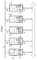
- Figure 1 shows a block diagram of a time switch system with exploded architecture.
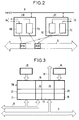
- FIG. 2 shows a block diagram of the switch in Figure 1.
- Figure 3 shows a diagram of a connection module according to the invention.
- FIG. 1 corresponds for example to a digital switch for a private telephone installation, it is assumed to serve telephone equipment connected to the switch via various digital or digital transmission links on arrival which are referenced 1A to 1E in Figure 1.
- Some of these links are for example standardized time-division multiplex links complying with the recommendation G.704 mentioned above, others are possibly time-division multiplex links having a different frame structure.
- Each link is intended to serve an item of equipment, for example a trunk of a remote switch or even a local control arrangement, it leads to a connection module in the local time switch presented here.
- time multiplex link 1A presented in FIG. 1 is assumed to connect a local connection module 2A to the control arrangement of the local time switch, this control arrangement generally being organized in a conventional manner around at least one processor 3 and a local clock 4.
- the other time multiplex links referenced 1B to 1E are here supposed to connect local connection modules referenced 2B to 2E to complementary connection modules and most often distant from the equipment served, these additional modules and the equipment served not being represented here. .
- All local connection modules 2A to 2E are connected to the same time-division multiplex link, of the bidirectional bus type, called the data bus and referenced 5, so as to allow an exchange of data by this data bus 5 between the devices they serve respectively.
- the data bus 5 is managed by a control structure which is here constituted by the control arrangement mentioned above which we have seen was organized around at least one processor 3 and a clock 4, it being understood that other known structures, not described here, are also capable of being implemented.
- the data bus 5 of the synchronous type is multifilar and ensures simultaneous transmission of several bits of the same information, in this case the bits of the same byte.
- This data bus supports a frame structure allowing
- each periodic frame of 125 ⁇ S is divided into 256 time intervals and allows the use of as many isochronous channels or consequently the serving of a plurality of connection modules connected to their respective equipment by time multiplex links supporting frame structures the number of channels of which is much less than 256 here, for example 32 per link.
- connection modules 2A to 2E concerned comprising for this purpose two associative memories connected on the one hand to the data bus 5 , on the other hand to the multiplex link leading to the connection module considered, such as the associative memories 6A and 7A connected both to the data bus 5 and to the link 1A for the connection module 2A.
- this is the control arrangement, here assumed to be organized around processor 3 and the clock 4, which manages the time switch with an exploded architecture that constitutes the data bus 5 and the connection modules 2A to 2E.
- the processor 3 is connected by an auxiliary signaling bus 8 to each of the connection modules 2B to 2E, connected to the data bus 5 and said to be local, for example through the control logic 9B to 9E associated with each connection module 2B to 2E in the local unit 10B to 10E of which this module is a part.
- the processor 4 here ensures the dynamic allocation of the time channels and consequently of the time intervals corresponding to the various connection modules on the data bus 5 as required, while the clock 3 provides, in a manner known to the tradesman, the corresponding time signals.
- the establishment of a communication between a local unit such as 10B and another local unit such as 10E implies the sending of a communication request by the logic 9B of the requesting local unit to the processor 4 via the auxiliary bus of signage 8.
- the processor 4 temporarily assigns one or more isochronous channels of the data bus 5 to the connection module 1B for its transmissions through its associative memory 6B according to a configuration table where the nominal requirements in terms of channels are recorded. transmission of all the connection modules and according to the channels, that is to say time slots on the data bus 5 which are then occupied for transmission by other connection modules.
- the channel or channels reserved for transmission for the connection module 5B via its associative memory 6B is or are also indicated in the receiver connection module 2E by processor 4 for reception of the corresponding data, via the associative memory 7E.
- connection module 2E and connection module 2B The same operations are undertaken to signal to the connection module 2E and to the connection module 2B the time intervals allocated to the transmissions from the first named to the second, such as the time interval IT20 in FIG. 2, via the respective associative memories 6E and 7B of these modules.
- associative memory 7, such as 7B, for connection module according to the invention is presented in FIG. 2, it is intended to ensure the transfers of data transmitted by the data bus 5, to which this associative memory is connected, to the particular time multiplex link 1, such as 1B, connecting the connection module in question to the equipment it serves.
- the associative memory 7B comprises an interval selection unit 11 essentially constituted by a plane of "n" comparator registers, such as the register 21 here only shown, which are intended to detect the occurrence of intervals of times determined during identical frames successively in force on the data bus 5.
- the selection unit 11 is connected to the processor 3 by the auxiliary signaling bus 8 and it receives from this processor the indication or indications relating to the time intervals allocated to a connection module entering into communication with the communication module which comprises it. via the data bus 5. This or these indications of time intervals are saved for the duration of the communication in each in a comparator register 21 of the unit 11.
- a counter 12 and a decoder, not shown, are associated with the associative memory 7B to cyclically scan all the time interval indications for the frame in force on the data bus 5, it is synchronized for this purpose by the clock signals supplied by the clock 4 which governs this bus.
- Each of the registers 21 of the selection unit 11 which contains an indication of time interval compares the indications successively supplied by the counter 12 with this indication which it stores in such a way as to allow data to be entered by the connection module 2B. transmitted to this module on the data bus 5 during the indicated time interval.
- the associative memory 7B comprises a data buffer unit 13 also composed of "n" registers 23 capable of each memorizing at least the data transmitted by the data bus destined for a connection module during a time interval, for example a byte.
- Each of the registers 23 of the data buffer unit 13 is connected to the data bus 5 by its data inputs and is write-activated by one of the registers 21 of the selection unit 11 detected by the latter of the arrival of the time interval which has been specifically indicated to it by the processor 3.
- a second counter 14 controls the reading of the data contained in the buffer unit 13, in association with a second time interval selection unit 15, in a manner analogous to that mentioned for the counter 12 and the first selection unit 11 of the associative memory 7B considered.
- the counter 14 is controlled by the clock signals in force on the particular multiplex link 1B served which are obtained by means of a conventional clock recovery device and not shown.
- the second interval selection unit 15 is identical to the first and therefore comprises a plane of "n" comparator registers 25, only one of which is differentiated here, these registers 25 are intended to detect the occurrence of time intervals determined in the course of identical frames successively in force on the particular time-division multiplex link 1B.
- the second selection unit 15 is connected to processor 3 by the auxiliary signaling bus 8 and it receives from this processor the indication or indications relating to the time intervals allocated to the equipment served on the multiplex link 1B for each of its communications with the connection module which includes this selection unit 15.
- This or these time interval indications are saved for the duration of the communication each in a comparator register 25 of the unit 15.
- a control buffer unit 16 is also included in the associative memory 7B, it includes "n" control registers 56, only one of which is differentiated here, these registers 56 are individually associated with the registers of the data buffer unit 13 likewise as the registers of selection units 11 and 15.
- Each register of the unit 16 is connected to the processor 3 via the auxiliary signaling bus 8 so as to receive command indications indicating the operations to be carried out at the corresponding register of the data buffer unit.
Landscapes
- Engineering & Computer Science (AREA)
- Computer Networks & Wireless Communication (AREA)
- Time-Division Multiplex Systems (AREA)
- Use Of Switch Circuits For Exchanges And Methods Of Control Of Multiplex Exchanges (AREA)
- Multi Processors (AREA)
- Electric Clocks (AREA)
Applications Claiming Priority (2)
| Application Number | Priority Date | Filing Date | Title |
|---|---|---|---|
| FR9014525 | 1990-11-21 | ||
| FR9014525A FR2669496B1 (fr) | 1990-11-21 | 1990-11-21 | Commutateur temporel a architecture eclatee et module de raccordement pour la constitution d'un tel commutateur. |
Publications (2)
| Publication Number | Publication Date |
|---|---|
| EP0487042A1 true EP0487042A1 (de) | 1992-05-27 |
| EP0487042B1 EP0487042B1 (de) | 1997-03-19 |
Family
ID=9402434
Family Applications (1)
| Application Number | Title | Priority Date | Filing Date |
|---|---|---|---|
| EP91119750A Expired - Lifetime EP0487042B1 (de) | 1990-11-21 | 1991-11-19 | Zeitmultiplexkoppelanordnung mit verteilter Architektur und einem Verbindungsmodul zur Bildung dieser Anordnung |
Country Status (8)
| Country | Link |
|---|---|
| US (1) | US5283786A (de) |
| EP (1) | EP0487042B1 (de) |
| JP (1) | JP2889027B2 (de) |
| AT (1) | ATE150608T1 (de) |
| CA (1) | CA2055923C (de) |
| DE (1) | DE69125247T2 (de) |
| ES (1) | ES2100196T3 (de) |
| FR (1) | FR2669496B1 (de) |
Families Citing this family (10)
| Publication number | Priority date | Publication date | Assignee | Title |
|---|---|---|---|---|
| USRE39395E1 (en) | 1992-11-02 | 2006-11-14 | Negotiated Data Solutions Llc | Data communication network with transfer port, cascade port and/or frame synchronizing signal |
| EP0596648A1 (de) | 1992-11-02 | 1994-05-11 | National Semiconductor Corporation | Erkennung du Fähigkeiten eines Netzendpunkts |
| USRE39116E1 (en) | 1992-11-02 | 2006-06-06 | Negotiated Data Solutions Llc | Network link detection and generation |
| EP0596651A1 (de) * | 1992-11-02 | 1994-05-11 | National Semiconductor Corporation | Datennetz mit isochroner Übertragungsfähigkeit |
| WO1996007139A1 (en) * | 1994-09-01 | 1996-03-07 | Mcalpine Gary L | A multi-port memory system including read and write buffer interfaces |
| US5533018A (en) | 1994-12-21 | 1996-07-02 | National Semiconductor Corporation | Multi-protocol packet framing over an isochronous network |
| US6070213A (en) * | 1997-12-30 | 2000-05-30 | Dsc Telecom L.P. | Telecommunications terminal |
| US7230927B1 (en) * | 1999-12-07 | 2007-06-12 | Aspect Software, Inc. | Non-blocking expandable call center architecture |
| JP2003324464A (ja) * | 2002-04-30 | 2003-11-14 | Fujitsu Ltd | データ検索装置及びデータ検索方法 |
| US9460159B1 (en) * | 2013-08-14 | 2016-10-04 | Google Inc. | Detecting visibility of a content item using tasks triggered by a timer |
Citations (2)
| Publication number | Priority date | Publication date | Assignee | Title |
|---|---|---|---|---|
| FR2119417A5 (de) * | 1970-12-24 | 1972-08-04 | Ibm | |
| EP0184774A2 (de) * | 1984-12-14 | 1986-06-18 | Alcatel N.V. | Speicheranordnung und eine Speicheranordnung enthaltende Koppelstufe zum Herstellen von dynamisch zugeordneten Verbindungswegen |
Family Cites Families (5)
| Publication number | Priority date | Publication date | Assignee | Title |
|---|---|---|---|---|
| US4127742A (en) * | 1977-09-01 | 1978-11-28 | International Telephone And Telegraph Corporation | Time division telecommunication system |
| EP0122684B1 (de) * | 1983-01-18 | 1988-06-15 | Plessey Overseas Limited | Elektronisches Vermittlungssystem |
| SE440580B (sv) * | 1983-12-15 | 1985-08-05 | Ericsson Telefon Ab L M | Anordning vid digitalt telefonsystem |
| US4674083A (en) * | 1984-11-16 | 1987-06-16 | Solid State Systems, Inc. | Time division multiplexed switching structure for PBX |
| US4809270A (en) * | 1984-12-21 | 1989-02-28 | AT&T Information Systems Inc. American Telephone and Telegraph Company | Variable time slot communication system |
-
1990
- 1990-11-21 FR FR9014525A patent/FR2669496B1/fr not_active Expired - Fee Related
-
1991
- 1991-11-19 DE DE69125247T patent/DE69125247T2/de not_active Expired - Fee Related
- 1991-11-19 AT AT91119750T patent/ATE150608T1/de not_active IP Right Cessation
- 1991-11-19 ES ES91119750T patent/ES2100196T3/es not_active Expired - Lifetime
- 1991-11-19 EP EP91119750A patent/EP0487042B1/de not_active Expired - Lifetime
- 1991-11-20 CA CA002055923A patent/CA2055923C/fr not_active Expired - Fee Related
- 1991-11-20 US US07/796,060 patent/US5283786A/en not_active Expired - Fee Related
- 1991-11-21 JP JP3306424A patent/JP2889027B2/ja not_active Expired - Fee Related
Patent Citations (2)
| Publication number | Priority date | Publication date | Assignee | Title |
|---|---|---|---|---|
| FR2119417A5 (de) * | 1970-12-24 | 1972-08-04 | Ibm | |
| EP0184774A2 (de) * | 1984-12-14 | 1986-06-18 | Alcatel N.V. | Speicheranordnung und eine Speicheranordnung enthaltende Koppelstufe zum Herstellen von dynamisch zugeordneten Verbindungswegen |
Non-Patent Citations (1)
| Title |
|---|
| INTERNATIONAL SWITCHING SYMPOSIUM, Kyoto, 25-29 octobre 1976, vol. 1, session 231-3, pages 1-6; I. ANDERSSON et al.: "HUGIN - a high speed unibus group selector for integrated digital networks" * |
Also Published As
| Publication number | Publication date |
|---|---|
| ATE150608T1 (de) | 1997-04-15 |
| JPH04287494A (ja) | 1992-10-13 |
| FR2669496A1 (fr) | 1992-05-22 |
| EP0487042B1 (de) | 1997-03-19 |
| DE69125247D1 (de) | 1997-04-24 |
| JP2889027B2 (ja) | 1999-05-10 |
| ES2100196T3 (es) | 1997-06-16 |
| CA2055923C (fr) | 1995-04-11 |
| FR2669496B1 (fr) | 1995-03-31 |
| US5283786A (en) | 1994-02-01 |
| CA2055923A1 (fr) | 1992-05-22 |
| DE69125247T2 (de) | 1997-06-26 |
Similar Documents
| Publication | Publication Date | Title |
|---|---|---|
| US5150357A (en) | Integrated communications system | |
| EP0036808B1 (de) | Konzentrator für Kommunikationssystem zum Anschliessen mehrerer asynchroner Telematik-Terminals | |
| US5228076A (en) | High fidelity speech encoding for telecommunications systems | |
| EP0034514A1 (de) | Digitale Zeitvielfach-Vermittlungsanlage für Leitungen mit Sprach- und Datenpaketübertragungen | |
| FR2748172A1 (fr) | Equipement d'adaptation de protocole pour poste telephonique et poste equipe d'un tel equipement | |
| EP0487042B1 (de) | Zeitmultiplexkoppelanordnung mit verteilter Architektur und einem Verbindungsmodul zur Bildung dieser Anordnung | |
| EP0504014B1 (de) | Verfahren und Vorrichtung zur Konzentration von Paketen für ISDN-Datenendgeräte | |
| EP0254920B1 (de) | System zum Anschluss von Telefonteilnehmern, rund um eine digitale Zeitmultiplexvermittlungsanlage gestaltet | |
| EP0645902B1 (de) | Satellitenanordnung für Datenübertragung zwischen Telefonvermittlungstellen, Verkehrstation und Übertragungsverfahren dafür | |
| US4811332A (en) | Apparatus and method for TDM data switching | |
| EP0161162B1 (de) | Automatische Vermittlungsanlage mit Video-Schaltmatrix | |
| EP0403998B1 (de) | Aufbau einer Fernprechnebenstellenanlage | |
| EP0610106B1 (de) | Signalierungsverarbeitungssystem für gemeinsame Unterstützung der Durchschaltebetriebsart in einer Telekommunikationsanlage | |
| EP0091327B1 (de) | Videokonferenzsystem für mehrere Säle | |
| EP0466590B1 (de) | Digitales Kommunikationssystem für eine digitale dienstintegrierte Fernsprechanlage | |
| FR2665314A1 (fr) | Reseau d'interconnexion pour cóoeur d'installation de communication et installation dotee d'un tel reseau. | |
| EP0530098B1 (de) | Verfahren und Anordnung für Nachrichtenübertragung zwischen Geräten einer Kommunikationsanlage | |
| JPS6147477B2 (de) | ||
| KR950035219A (ko) | 종합정보통신망과 근거리통신망 간의 망정합을 위한 게이트웨이 구현방법 및 시스템 | |
| EP0443482A1 (de) | Anordnung zum Anschluss digitaler Endstationen an eine einzige Schnittstelle höherer Geschwindigkeit | |
| FR2693064A1 (fr) | Dispositif de télécommande pour installation d'abonné d'un réseau numérique à intégration de services. | |
| EP0101357A1 (de) | Automatisches elektronisches Zeitmultiplex-Vermittlungssystem, modular in Verkehrsleistung und Kapazität | |
| FR2706722A1 (fr) | Procédé et agencement pour une transmission en mode cellule d'informations fournies et restituées en mode à bande étroite. | |
| KR20010063838A (ko) | 비 채널 데이터 교환 장치 및 그를 이용한종합정보통신망용 단말기 | |
| FR2675605A1 (fr) | Procede et dispositif d'adressage de peripheriques pour le partage d'un canal de transmission de donnees entre les peripheriques. |
Legal Events
| Date | Code | Title | Description |
|---|---|---|---|
| PUAI | Public reference made under article 153(3) epc to a published international application that has entered the european phase |
Free format text: ORIGINAL CODE: 0009012 |
|
| AK | Designated contracting states |
Kind code of ref document: A1 Designated state(s): AT BE CH DE DK ES FR GB IT LI NL SE |
|
| 17P | Request for examination filed |
Effective date: 19921124 |
|
| 17Q | First examination report despatched |
Effective date: 19950215 |
|
| GRAG | Despatch of communication of intention to grant |
Free format text: ORIGINAL CODE: EPIDOS AGRA |
|
| GRAH | Despatch of communication of intention to grant a patent |
Free format text: ORIGINAL CODE: EPIDOS IGRA |
|
| GRAH | Despatch of communication of intention to grant a patent |
Free format text: ORIGINAL CODE: EPIDOS IGRA |
|
| GRAA | (expected) grant |
Free format text: ORIGINAL CODE: 0009210 |
|
| AK | Designated contracting states |
Kind code of ref document: B1 Designated state(s): AT BE CH DE DK ES FR GB IT LI NL SE |
|
| PG25 | Lapsed in a contracting state [announced via postgrant information from national office to epo] |
Ref country code: DK Effective date: 19970319 |
|
| REF | Corresponds to: |
Ref document number: 150608 Country of ref document: AT Date of ref document: 19970415 Kind code of ref document: T |
|
| REG | Reference to a national code |
Ref country code: CH Ref legal event code: EP |
|
| REG | Reference to a national code |
Ref country code: CH Ref legal event code: NV Representative=s name: GEC ALSTHOM (SUISSE) S.A. DEPARTEMENT DES BREVETS |
|
| REF | Corresponds to: |
Ref document number: 69125247 Country of ref document: DE Date of ref document: 19970424 |
|
| ITF | It: translation for a ep patent filed | ||
| REG | Reference to a national code |
Ref country code: ES Ref legal event code: FG2A Ref document number: 2100196 Country of ref document: ES Kind code of ref document: T3 |
|
| GBT | Gb: translation of ep patent filed (gb section 77(6)(a)/1977) |
Effective date: 19970612 |
|
| PLBE | No opposition filed within time limit |
Free format text: ORIGINAL CODE: 0009261 |
|
| STAA | Information on the status of an ep patent application or granted ep patent |
Free format text: STATUS: NO OPPOSITION FILED WITHIN TIME LIMIT |
|
| 26N | No opposition filed | ||
| PGFP | Annual fee paid to national office [announced via postgrant information from national office to epo] |
Ref country code: CH Payment date: 20011016 Year of fee payment: 11 |
|
| PGFP | Annual fee paid to national office [announced via postgrant information from national office to epo] |
Ref country code: AT Payment date: 20011026 Year of fee payment: 11 |
|
| PGFP | Annual fee paid to national office [announced via postgrant information from national office to epo] |
Ref country code: NL Payment date: 20011031 Year of fee payment: 11 |
|
| PGFP | Annual fee paid to national office [announced via postgrant information from national office to epo] |
Ref country code: SE Payment date: 20011105 Year of fee payment: 11 |
|
| PGFP | Annual fee paid to national office [announced via postgrant information from national office to epo] |
Ref country code: BE Payment date: 20011114 Year of fee payment: 11 |
|
| REG | Reference to a national code |
Ref country code: GB Ref legal event code: IF02 |
|
| PG25 | Lapsed in a contracting state [announced via postgrant information from national office to epo] |
Ref country code: AT Free format text: LAPSE BECAUSE OF NON-PAYMENT OF DUE FEES Effective date: 20021119 |
|
| PG25 | Lapsed in a contracting state [announced via postgrant information from national office to epo] |
Ref country code: SE Free format text: LAPSE BECAUSE OF NON-PAYMENT OF DUE FEES Effective date: 20021120 |
|
| PG25 | Lapsed in a contracting state [announced via postgrant information from national office to epo] |
Ref country code: LI Free format text: LAPSE BECAUSE OF NON-PAYMENT OF DUE FEES Effective date: 20021130 Ref country code: CH Free format text: LAPSE BECAUSE OF NON-PAYMENT OF DUE FEES Effective date: 20021130 Ref country code: BE Free format text: LAPSE BECAUSE OF NON-PAYMENT OF DUE FEES Effective date: 20021130 |
|
| BERE | Be: lapsed |
Owner name: *ALCATEL BUSINESS SYSTEMS Effective date: 20021130 |
|
| PG25 | Lapsed in a contracting state [announced via postgrant information from national office to epo] |
Ref country code: NL Free format text: LAPSE BECAUSE OF NON-PAYMENT OF DUE FEES Effective date: 20030601 |
|
| EUG | Se: european patent has lapsed | ||
| REG | Reference to a national code |
Ref country code: CH Ref legal event code: PL |
|
| NLV4 | Nl: lapsed or anulled due to non-payment of the annual fee |
Effective date: 20030601 |
|
| PGFP | Annual fee paid to national office [announced via postgrant information from national office to epo] |
Ref country code: GB Payment date: 20031029 Year of fee payment: 13 |
|
| PGFP | Annual fee paid to national office [announced via postgrant information from national office to epo] |
Ref country code: DE Payment date: 20031103 Year of fee payment: 13 |
|
| PGFP | Annual fee paid to national office [announced via postgrant information from national office to epo] |
Ref country code: FR Payment date: 20031107 Year of fee payment: 13 |
|
| PGFP | Annual fee paid to national office [announced via postgrant information from national office to epo] |
Ref country code: ES Payment date: 20031119 Year of fee payment: 13 |
|
| PG25 | Lapsed in a contracting state [announced via postgrant information from national office to epo] |
Ref country code: GB Free format text: LAPSE BECAUSE OF NON-PAYMENT OF DUE FEES Effective date: 20041119 |
|
| PG25 | Lapsed in a contracting state [announced via postgrant information from national office to epo] |
Ref country code: ES Free format text: LAPSE BECAUSE OF NON-PAYMENT OF DUE FEES Effective date: 20041120 |
|
| PG25 | Lapsed in a contracting state [announced via postgrant information from national office to epo] |
Ref country code: DE Free format text: LAPSE BECAUSE OF NON-PAYMENT OF DUE FEES Effective date: 20050601 |
|
| GBPC | Gb: european patent ceased through non-payment of renewal fee |
Effective date: 20041119 |
|
| PG25 | Lapsed in a contracting state [announced via postgrant information from national office to epo] |
Ref country code: FR Free format text: LAPSE BECAUSE OF NON-PAYMENT OF DUE FEES Effective date: 20050729 |
|
| REG | Reference to a national code |
Ref country code: FR Ref legal event code: ST |
|
| PG25 | Lapsed in a contracting state [announced via postgrant information from national office to epo] |
Ref country code: IT Free format text: LAPSE BECAUSE OF NON-PAYMENT OF DUE FEES;WARNING: LAPSES OF ITALIAN PATENTS WITH EFFECTIVE DATE BEFORE 2007 MAY HAVE OCCURRED AT ANY TIME BEFORE 2007. THE CORRECT EFFECTIVE DATE MAY BE DIFFERENT FROM THE ONE RECORDED. Effective date: 20051119 |
|
| REG | Reference to a national code |
Ref country code: ES Ref legal event code: FD2A Effective date: 20041120 |