EP0487143B1 - Spectromètre - Google Patents
Spectromètre Download PDFInfo
- Publication number
- EP0487143B1 EP0487143B1 EP91202957A EP91202957A EP0487143B1 EP 0487143 B1 EP0487143 B1 EP 0487143B1 EP 91202957 A EP91202957 A EP 91202957A EP 91202957 A EP91202957 A EP 91202957A EP 0487143 B1 EP0487143 B1 EP 0487143B1
- Authority
- EP
- European Patent Office
- Prior art keywords
- charge
- detector
- charges
- spectrometer
- transistor
- Prior art date
- Legal status (The legal status is an assumption and is not a legal conclusion. Google has not performed a legal analysis and makes no representation as to the accuracy of the status listed.)
- Expired - Lifetime
Links
Images

Classifications
-
- G—PHYSICS
- G01—MEASURING; TESTING
- G01J—MEASUREMENT OF INTENSITY, VELOCITY, SPECTRAL CONTENT, POLARISATION, PHASE OR PULSE CHARACTERISTICS OF INFRARED, VISIBLE OR ULTRAVIOLET LIGHT; COLORIMETRY; RADIATION PYROMETRY
- G01J1/00—Photometry, e.g. photographic exposure meter
- G01J1/42—Photometry, e.g. photographic exposure meter using electric radiation detectors
- G01J1/44—Electric circuits
-
- G—PHYSICS
- G01—MEASURING; TESTING
- G01J—MEASUREMENT OF INTENSITY, VELOCITY, SPECTRAL CONTENT, POLARISATION, PHASE OR PULSE CHARACTERISTICS OF INFRARED, VISIBLE OR ULTRAVIOLET LIGHT; COLORIMETRY; RADIATION PYROMETRY
- G01J3/00—Spectrometry; Spectrophotometry; Monochromators; Measuring colours
- G01J3/28—Investigating the spectrum
- G01J3/2803—Investigating the spectrum using photoelectric array detector
Definitions
- the invention relates to a spectrometer comprising means for directing radiation emanating from or passing through a sample onto a radiation detector, signal processing means for processing the signal produced by the radiation detector, and display means for displaying the processed signal, wherein the detector comprises an m column by n row array of charge coupled devices, means for accumulating the charges from a plurality of devices on an output capacitor, and means for producing an output signal representing the charge on the output capacitor.
- This technique can only be applied where either a small number of detector elements which accumulate a maximum charge are binned or if a large number of detector elements are binned each detector element can only accumulate a small charge. This is because in one direction of the array the shift register can only hold a small amount of charge, typically between one and five times the maximum detector element charge, and in the other direction the output capacitor has a small charge handling capacity, again typically not more than five times a shift register stage charge.
- the invention provides a spectrometer as set forth in the opening paragraph characterised in that a further, external, capacitor is connected in series with said output capacitor.
- CCDs are commonly used for capturing the image in video cameras and are commonly made in arrays of 600 by 575 detector elements (or pixels in television terminology), see for example the Philips NXA 1001 solid state image sensor.
- a polychromator disperses the radiation and causes a narrowband of wavelengths to illuminate each column of the detector.
- Possible alternatives are to restrict the energy of the radiation so that no detector element accumulates a large charge regardless of the absorbance of the sample or the integration time or to read out individual or a small number of detector elements and sum them digitally.
- the first alternative suffers from the disadvantage that when there is significant sample absorbance the radiation received by the detector will be very low and hence will result in reduced sensitivity and increased noise.
- the second alternative has the disadvantage of increasing the read out noise as discussed hereinbefore. By adding extra external capacitance it is possible to sum the charges from many picture elements as the external capacitor can be made much larger than the "on chip" output capacitor provided in the CCD.
- the invention allows the use of low cost standard CCD chips designed for consumer applications such as video cameras as detectors for spectrometers and enables the signal to be read out with a minimum of added noise.
- the charges from a complete column of detector elements may be accumulated on said capacitors and the output signal produced when said charges have been accumulated. This enables a maximum sensitivity of measurement since when low level signals are received at the detector a large detector area is available which maximises the total radiation received and for signal shot noise limited operation as the signal increases the noise increases as the square root of the signal and hence the signal to noise ratio is increased.
- the charges from a selected number of the detector elements of a column may be accumulated on said capacitors and the output signal produced when said charges have been accumulated.
- the spectrometer may include a transistor connected to the parallel arrangement of said capacitors and control means for controlling the transistor to cause it to reset the capacitors to a given state of charge when the output signal has been produced.
- the pixel reset transistor is isolated from the reference supply and instead of resetting the internal capacitor it causes charge sharing between the internal and external capacitors.
- the resetting function is then performed by the external transistor which serves to isolate the internal transistor from the reference voltage source used to reset the capacitors to a given charge state.
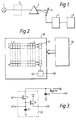
- the spectrometer comprises a radiation source 1 which emits wideband radiation.
- a radiation source 1 which emits wideband radiation.
- Many such sources are known, for example tungsten filament lamps for visible wavelengths or deuterium lamps for ultra violet (UV) wavelengths.
- the radiation from the source 1 is directed through a sample compartment 2 onto a dispersing element 3.
- the radiation is directed through the sample compartment by appropriate optical means, mirrors and/or lenses, onto the dispersing means which may be a prism or a diffraction grating.
- appropriate optical elements are used to collimate and focus the radiation beam where appropriate.
- the dispersed radiation beam is directed onto a detector 4 which comprises a charge coupled device array.
- the detector 4 comprises a regular array of m rows by n columns of charge coupled devices as is conventionally used in television cameras.
- a control and signal processing circuit 5 provides the necessary signals to read the output of the detector 4 and processes the signal read out for display on a display device 6.
- the display devices 6 may take any convenient
- Figure 2 shows the detector 4 which is in the form of a charge coupled device in the form of an array 50 having n columns of m charge coupled devices.
- An output shift register 51 is connected to an output circuit 52 which produces an output signal at an output terminal 53.
- the detector 4 may comprise a commercially available CCD array and has associated with it control circuitry 54 to enable the charge to be accumulated and readout. Details of such control circuitry are readily available, for example in a data handbook entitled Solid State Image Sensors and Peripheral Integrated Circuits published by Philips Components (Book PC11, 1989).
- the control circuitry produces appropriate clocking and readout signals which cause the charges from each device to be read in sequence one column at a time in parallel into the shift register 51 from where it is shifted serially into the output circuit 52 from which it is fed to output 53 for connection to the control and processing circuit 5.
- Figure 3 shows how the output circuit 52 is modified to allow binning of all the charges in a column or of a substantial portion of them regardless of the charge accumulated by each of the elements.
- the dotted box 52 represents the output circuit shown in Figure 2.
- a first input 61 is connected to the junction of a capacitor C1 and the source electrode of an n-channel field effect transistor T1 and also to the gate electrode of an n-channel field effect transistor T2.
- the other end of the capacitor C1 is connected to a negative supply rail -V while the drain electrode of transistor T2 is connected to a positive supply rail +V.
- the drain electrode of transistor T1 is connected to the junction of a capacitor C2 and the source electrode of an n-channel field effect transistor T3.
- capacitor C2 is connected to the negative supply rail -V while the drain electrode of transistor T3 is connected to the a reference voltage V R .
- a second input 62 is connected to the gate electrode of transistor T1 while a third input 63 is connected to the gate electrode of transistor T3.
- the source electrode of transistor T2 is connected to the output terminal 53.
- charges from the shift register 51 are fed to the first input 61 while a pixel reset control signal is fed to the second input 62.
- a column reset control signal is fed to the third input 63.
- the drain electrode of transistor T1 would be connected directly to the reference voltage V R and consequently when the pixel reset pulses are received this would reset the charge on capacitor C1 to a given value.
- This charge is then incremented by each of the charge packets received from the shift register 51 at input 61.
- the pixel reset pulses are normally applied after receipt of each charge packet so that a series of pulses are produced at output 53 which correspond in magnitude to the magnitude of the individual charge packets. However, by reducing the frequency of the pixel reset pulses it is possible to accumulate a limited number of charge packets on the capacitor C1.
- the number is limited by the value of the capacitor C1, which cannot conveniently be made large by integrated circuit techniques, and the size of the charge packets, i.e. if it can be ensured that only a small charge accumulates on each element of the array then a greater number can be accumulated on capacitor C1.
- the arrangement shown in Figure 3 includes transistor T3 and capacitor C2 connected externally to the CCD array such that the transistor T3 is connected between the reference source V R and the drain electrode of transistor T1.
- Transistor T3 is controlled by a column reset signal applied to terminal 63 and isolates transistor T1 from the reference source V R except when the reset signal is present. Consequently as each charge packet is received it accumulates on capacitors C1 and C2 which are connected in parallel when transistor T1 is switched on by the pixel reset pulses.
- Capacitor C2 can be chosen to be much larger than capacitor C1 as it is realised as a discrete component. This charge is accumulated on the parallel combination of capacitors C1 and C2 and a whole column of CCDs can be binned in this combination even when all the elements have accumulated their maximum charge.
- Figure 4 is a timing diagram showing in Figure 4a) the charge packets applied to input 61, in Figure 4b) the pixel reset pulses applied to input 62, in Figure 4c) the column reset pulses applied to input 63, and in Figure 4d) the output signal at terminal 53.
- Figure 1 is a typical construction of an optical spectrometer used for measuring the absorbance or transmittance of a sample by passing radiation from a source through a sample to a detector
- the invention is also applicable to spectrometers where the detector receives radiation emitted by the sample either by direct emission such as in atomic emission spectrometers or by emission in response to exciting radiation such as in X-ray fluorescence or atomic fluorescence spectrometers.
Landscapes
- Physics & Mathematics (AREA)
- Spectroscopy & Molecular Physics (AREA)
- General Physics & Mathematics (AREA)
- Spectrometry And Color Measurement (AREA)
- Transforming Light Signals Into Electric Signals (AREA)
Claims (4)
- Spectromètre comprenant des moyens pour diriger un rayonnement émanant d'un échantillon ou passant à travers un échantillon sur un détecteur de rayonnement, des moyens de traitement de signaux pour traiter le signal produit par le détecteur de rayonnement, et des moyens d'affichage pour afficher le signal traité, dans lequel le détecteur comprend une matrice de m colonnes sur n rangées de dispositifs à couplage de charges, des moyens pour accumuler les charges issues d'une pluralité de dispositifs sur un condensateur de sortie, et des moyens pour produire un signal de sortie représentant la charge sur le condensateur de sortie.
- Spectromètre selon la revendication 1, dans lequel les charges provenant d'une colonne complète d'éléments de détection sont accumulées sur lesdits condensateurs, le signal de sortie étant produit lorsque lesdites charges ont été accumulées.
- Spectromètre selon la revendication 1, dans lequel les charges provenant d'un nombre sélectionné des éléments de détection d'une colonne sont accumulées sur lesdits condensateurs le signal de sortie étant produit lorsque lesdites charges ont été accumulées.
- Spectromètre selon l'une quelconque des revendications 1 à 3, comprenant un transistor connecté à l'agencement en parallèle desdits condensateurs et des moyens de commande pour commander le transistor afin de le forcer à ramener les condensateurs dans un état de charge donné lorsque le signal de sortie a été produit.
Applications Claiming Priority (2)
| Application Number | Priority Date | Filing Date | Title |
|---|---|---|---|
| GB9025345A GB2250089A (en) | 1990-11-21 | 1990-11-21 | Spectrometer |
| GB9025345 | 1990-11-21 |
Publications (3)
| Publication Number | Publication Date |
|---|---|
| EP0487143A2 EP0487143A2 (fr) | 1992-05-27 |
| EP0487143A3 EP0487143A3 (en) | 1992-09-02 |
| EP0487143B1 true EP0487143B1 (fr) | 1995-02-22 |
Family
ID=10685764
Family Applications (1)
| Application Number | Title | Priority Date | Filing Date |
|---|---|---|---|
| EP91202957A Expired - Lifetime EP0487143B1 (fr) | 1990-11-21 | 1991-11-14 | Spectromètre |
Country Status (5)
| Country | Link |
|---|---|
| US (1) | US5235402A (fr) |
| EP (1) | EP0487143B1 (fr) |
| JP (1) | JPH04268422A (fr) |
| DE (1) | DE69107583T2 (fr) |
| GB (1) | GB2250089A (fr) |
Families Citing this family (4)
| Publication number | Priority date | Publication date | Assignee | Title |
|---|---|---|---|---|
| US5493122A (en) * | 1994-02-04 | 1996-02-20 | Nucleonics Development Company | Energy resolving x-ray detector |
| US5590660A (en) * | 1994-03-28 | 1997-01-07 | Xillix Technologies Corp. | Apparatus and method for imaging diseased tissue using integrated autofluorescence |
| DE4413096B4 (de) * | 1994-04-15 | 2004-09-09 | Berthold Gmbh & Co. Kg | Multielement-Atomabsorptionsspektrometer sowie Meßverfahren unter Nutzung eines solchen Atomabsorptionsspektrometers |
| US7084973B1 (en) | 2002-06-11 | 2006-08-01 | Dalsa Inc. | Variable binning CCD for spectroscopy |
Family Cites Families (3)
| Publication number | Priority date | Publication date | Assignee | Title |
|---|---|---|---|---|
| US4004163A (en) * | 1976-03-11 | 1977-01-18 | Rockwell International Corporation | Time delay, charge, transfer circuit |
| JPS6134798A (ja) * | 1984-07-25 | 1986-02-19 | Sharp Corp | 電荷転送素子の出力信号処理回路 |
| ES2035985T3 (es) * | 1989-05-20 | 1993-05-01 | Hewlett-Packard Gmbh | Metodo de funcionamiento de un espectometro de fotodiodos y espectrometro de fotodiodos correspondiente. |
-
1990
- 1990-11-21 GB GB9025345A patent/GB2250089A/en not_active Withdrawn
-
1991
- 1991-11-14 DE DE69107583T patent/DE69107583T2/de not_active Expired - Fee Related
- 1991-11-14 EP EP91202957A patent/EP0487143B1/fr not_active Expired - Lifetime
- 1991-11-18 US US07/795,166 patent/US5235402A/en not_active Expired - Fee Related
- 1991-11-20 JP JP3304824A patent/JPH04268422A/ja active Pending
Also Published As
| Publication number | Publication date |
|---|---|
| JPH04268422A (ja) | 1992-09-24 |
| GB2250089A (en) | 1992-05-27 |
| DE69107583T2 (de) | 1995-09-07 |
| GB9025345D0 (en) | 1991-01-02 |
| EP0487143A2 (fr) | 1992-05-27 |
| DE69107583D1 (de) | 1995-03-30 |
| US5235402A (en) | 1993-08-10 |
| EP0487143A3 (en) | 1992-09-02 |
Similar Documents
| Publication | Publication Date | Title |
|---|---|---|
| EP0316802B1 (fr) | Détecteur pour un spectromètre | |
| US7154548B2 (en) | Multiplexed and pipelined column buffer for use with an array of photo sensors | |
| US4996413A (en) | Apparatus and method for reading data from an image detector | |
| EP0773669B1 (fr) | Circuit, élément d'image, dispositif et méthode pour la réduction du motif de bruit fixe dans des dispositifs de prise d'images à l'état solide | |
| US7791657B2 (en) | Dynamic range enhancement scheme for imagers | |
| CN1817027B (zh) | 用于提高基于电荷耦合器件的光谱仪的动态范围的装置和方法 | |
| US4245158A (en) | Soft x-ray spectrometric imaging system | |
| US5953060A (en) | Method for reducing fixed pattern noise in solid state imaging devices | |
| US4617593A (en) | Visible and near infrared imaging system | |
| WO2001045392A2 (fr) | Détecteur d'images | |
| JP3143747B2 (ja) | フォトダイオード・アレイ分光検出器とフォトダイオード・アレイ分光検出器を操作する方法 | |
| EP0355174B1 (fr) | Spectromètre à réseau de photodiodes | |
| US20210185199A1 (en) | Random Access Sensor | |
| EP0904655B1 (fr) | Procede et systeme d'etalonnage pour dispositifs de formation d'images | |
| US5149954A (en) | Hold capacitor time delay and integration with equilibrating means | |
| US7084973B1 (en) | Variable binning CCD for spectroscopy | |
| EP0967794B1 (fr) | Réseau de photodiodes | |
| EP0487143B1 (fr) | Spectromètre | |
| Treis et al. | First results of DEPFET-based active-pixel-sensor prototypes for the XEUS wide-field imager | |
| Shectman | A two-dimensional photon counter | |
| Leach | Optimizing charge-coupled-device detector operation for optical astronomy | |
| US5430294A (en) | Staring focal plane array architecture for multiple applications | |
| US4667239A (en) | Signal peaking device for single-line video input | |
| US5254848A (en) | Image sensor and method of reading data out of the same having load capacitors being respectively continuously connected to common signal lines | |
| Glass et al. | An infrared camera based on a large PtSi array |
Legal Events
| Date | Code | Title | Description |
|---|---|---|---|
| PUAI | Public reference made under article 153(3) epc to a published international application that has entered the european phase |
Free format text: ORIGINAL CODE: 0009012 |
|
| AK | Designated contracting states |
Kind code of ref document: A2 Designated state(s): DE FR GB |
|
| PUAL | Search report despatched |
Free format text: ORIGINAL CODE: 0009013 |
|
| AK | Designated contracting states |
Kind code of ref document: A3 Designated state(s): DE FR GB |
|
| 17P | Request for examination filed |
Effective date: 19930223 |
|
| 17Q | First examination report despatched |
Effective date: 19940412 |
|
| GRAA | (expected) grant |
Free format text: ORIGINAL CODE: 0009210 |
|
| AK | Designated contracting states |
Kind code of ref document: B1 Designated state(s): DE FR GB |
|
| REF | Corresponds to: |
Ref document number: 69107583 Country of ref document: DE Date of ref document: 19950330 |
|
| ET | Fr: translation filed | ||
| PLBE | No opposition filed within time limit |
Free format text: ORIGINAL CODE: 0009261 |
|
| STAA | Information on the status of an ep patent application or granted ep patent |
Free format text: STATUS: NO OPPOSITION FILED WITHIN TIME LIMIT |
|
| PGFP | Annual fee paid to national office [announced via postgrant information from national office to epo] |
Ref country code: DE Payment date: 19960125 Year of fee payment: 5 |
|
| 26N | No opposition filed | ||
| PGFP | Annual fee paid to national office [announced via postgrant information from national office to epo] |
Ref country code: GB Payment date: 19961101 Year of fee payment: 6 |
|
| PGFP | Annual fee paid to national office [announced via postgrant information from national office to epo] |
Ref country code: FR Payment date: 19961119 Year of fee payment: 6 |
|
| PG25 | Lapsed in a contracting state [announced via postgrant information from national office to epo] |
Ref country code: DE Effective date: 19970801 |
|
| PG25 | Lapsed in a contracting state [announced via postgrant information from national office to epo] |
Ref country code: GB Free format text: LAPSE BECAUSE OF NON-PAYMENT OF DUE FEES Effective date: 19971114 |
|
| PG25 | Lapsed in a contracting state [announced via postgrant information from national office to epo] |
Ref country code: FR Free format text: THE PATENT HAS BEEN ANNULLED BY A DECISION OF A NATIONAL AUTHORITY Effective date: 19971130 |
|
| GBPC | Gb: european patent ceased through non-payment of renewal fee |
Effective date: 19971114 |
|
| REG | Reference to a national code |
Ref country code: FR Ref legal event code: ST |